EP0571944A1 - Dispositif de conversion photoélectrique - Google Patents
Dispositif de conversion photoélectrique Download PDFInfo
- Publication number
- EP0571944A1 EP0571944A1 EP93108415A EP93108415A EP0571944A1 EP 0571944 A1 EP0571944 A1 EP 0571944A1 EP 93108415 A EP93108415 A EP 93108415A EP 93108415 A EP93108415 A EP 93108415A EP 0571944 A1 EP0571944 A1 EP 0571944A1
- Authority
- EP
- European Patent Office
- Prior art keywords
- photoelectric conversion
- layer
- conversion device
- carrier multiplication
- charge injection
- Prior art date
- Legal status (The legal status is an assumption and is not a legal conclusion. Google has not performed a legal analysis and makes no representation as to the accuracy of the status listed.)
- Granted
Links
- 238000006243 chemical reaction Methods 0.000 title claims abstract description 68
- 125000005842 heteroatom Chemical group 0.000 claims abstract description 24
- 239000002178 crystalline material Substances 0.000 claims abstract description 9
- 238000002347 injection Methods 0.000 claims description 25
- 239000007924 injection Substances 0.000 claims description 25
- 230000000903 blocking effect Effects 0.000 claims description 24
- 239000000463 material Substances 0.000 claims description 21
- 238000003860 storage Methods 0.000 claims description 13
- 229910006990 Si1-xGex Inorganic materials 0.000 claims description 12
- 229910007020 Si1−xGex Inorganic materials 0.000 claims description 12
- 229920001296 polysiloxane Polymers 0.000 claims description 8
- 239000013078 crystal Substances 0.000 claims description 7
- 125000004429 atom Chemical group 0.000 claims description 3
- 239000012535 impurity Substances 0.000 claims description 3
- UFHFLCQGNIYNRP-UHFFFAOYSA-N Hydrogen Chemical compound [H][H] UFHFLCQGNIYNRP-UHFFFAOYSA-N 0.000 claims description 2
- 229910052739 hydrogen Inorganic materials 0.000 claims description 2
- 239000001257 hydrogen Substances 0.000 claims description 2
- 125000004435 hydrogen atom Chemical group [H]* 0.000 claims 3
- 239000004065 semiconductor Substances 0.000 description 23
- 238000010586 diagram Methods 0.000 description 18
- 230000005684 electric field Effects 0.000 description 18
- 238000000098 azimuthal photoelectron diffraction Methods 0.000 description 16
- 230000000694 effects Effects 0.000 description 9
- 239000000969 carrier Substances 0.000 description 8
- BLRPTPMANUNPDV-UHFFFAOYSA-N Silane Chemical compound [SiH4] BLRPTPMANUNPDV-UHFFFAOYSA-N 0.000 description 7
- 239000007789 gas Substances 0.000 description 7
- 239000000203 mixture Substances 0.000 description 7
- 239000000758 substrate Substances 0.000 description 7
- QUZPNFFHZPRKJD-UHFFFAOYSA-N germane Chemical compound [GeH4] QUZPNFFHZPRKJD-UHFFFAOYSA-N 0.000 description 6
- 229910052986 germanium hydride Inorganic materials 0.000 description 6
- 229910021417 amorphous silicon Inorganic materials 0.000 description 5
- 230000015572 biosynthetic process Effects 0.000 description 5
- 239000003990 capacitor Substances 0.000 description 5
- 150000001875 compounds Chemical class 0.000 description 5
- 230000007423 decrease Effects 0.000 description 5
- 238000000034 method Methods 0.000 description 4
- 230000003247 decreasing effect Effects 0.000 description 3
- 230000003287 optical effect Effects 0.000 description 3
- 238000005268 plasma chemical vapour deposition Methods 0.000 description 3
- -1 cyclic silane compounds Chemical class 0.000 description 2
- 238000009413 insulation Methods 0.000 description 2
- 238000004544 sputter deposition Methods 0.000 description 2
- 229910006160 GeF4 Inorganic materials 0.000 description 1
- OAKJQQAXSVQMHS-UHFFFAOYSA-N Hydrazine Chemical compound NN OAKJQQAXSVQMHS-UHFFFAOYSA-N 0.000 description 1
- XYFCBTPGUUZFHI-UHFFFAOYSA-N Phosphine Chemical compound P XYFCBTPGUUZFHI-UHFFFAOYSA-N 0.000 description 1
- 229910007159 Si(CH3)4 Inorganic materials 0.000 description 1
- 229910007260 Si2F6 Inorganic materials 0.000 description 1
- 229910007264 Si2H6 Inorganic materials 0.000 description 1
- 229910005096 Si3H8 Inorganic materials 0.000 description 1
- 229910004014 SiF4 Inorganic materials 0.000 description 1
- 229910003824 SiH3F Inorganic materials 0.000 description 1
- 229910000577 Silicon-germanium Inorganic materials 0.000 description 1
- 230000003321 amplification Effects 0.000 description 1
- 229910052787 antimony Inorganic materials 0.000 description 1
- 229910052785 arsenic Inorganic materials 0.000 description 1
- 229910052797 bismuth Inorganic materials 0.000 description 1
- 150000001722 carbon compounds Chemical class 0.000 description 1
- 230000000593 degrading effect Effects 0.000 description 1
- RWRIWBAIICGTTQ-UHFFFAOYSA-N difluoromethane Chemical compound FCF RWRIWBAIICGTTQ-UHFFFAOYSA-N 0.000 description 1
- PZPGRFITIJYNEJ-UHFFFAOYSA-N disilane Chemical compound [SiH3][SiH3] PZPGRFITIJYNEJ-UHFFFAOYSA-N 0.000 description 1
- 230000002349 favourable effect Effects 0.000 description 1
- ZHPNWZCWUUJAJC-UHFFFAOYSA-N fluorosilicon Chemical compound [Si]F ZHPNWZCWUUJAJC-UHFFFAOYSA-N 0.000 description 1
- 229910052732 germanium Inorganic materials 0.000 description 1
- GNPVGFCGXDBREM-UHFFFAOYSA-N germanium atom Chemical compound [Ge] GNPVGFCGXDBREM-UHFFFAOYSA-N 0.000 description 1
- 150000002291 germanium compounds Chemical class 0.000 description 1
- 229910052736 halogen Inorganic materials 0.000 description 1
- 150000002367 halogens Chemical class 0.000 description 1
- 229910052738 indium Inorganic materials 0.000 description 1
- 229910003437 indium oxide Inorganic materials 0.000 description 1
- PJXISJQVUVHSOJ-UHFFFAOYSA-N indium(iii) oxide Chemical compound [O-2].[O-2].[O-2].[In+3].[In+3] PJXISJQVUVHSOJ-UHFFFAOYSA-N 0.000 description 1
- 239000012770 industrial material Substances 0.000 description 1
- 231100001231 less toxic Toxicity 0.000 description 1
- 238000004519 manufacturing process Methods 0.000 description 1
- 239000011159 matrix material Substances 0.000 description 1
- VNWKTOKETHGBQD-UHFFFAOYSA-N methane Chemical compound C VNWKTOKETHGBQD-UHFFFAOYSA-N 0.000 description 1
- 238000001451 molecular beam epitaxy Methods 0.000 description 1
- 229910017464 nitrogen compound Inorganic materials 0.000 description 1
- 150000002830 nitrogen compounds Chemical class 0.000 description 1
- 238000003199 nucleic acid amplification method Methods 0.000 description 1
- 150000002927 oxygen compounds Chemical class 0.000 description 1
- 229910052698 phosphorus Inorganic materials 0.000 description 1
- 230000006798 recombination Effects 0.000 description 1
- 238000005215 recombination Methods 0.000 description 1
- 150000004756 silanes Chemical class 0.000 description 1
- ABTOQLMXBSRXSM-UHFFFAOYSA-N silicon tetrafluoride Chemical compound F[Si](F)(F)F ABTOQLMXBSRXSM-UHFFFAOYSA-N 0.000 description 1
- KXCAEQNNTZANTK-UHFFFAOYSA-N stannane Chemical compound [SnH4] KXCAEQNNTZANTK-UHFFFAOYSA-N 0.000 description 1
- PPMWWXLUCOODDK-UHFFFAOYSA-N tetrafluorogermane Chemical compound F[Ge](F)(F)F PPMWWXLUCOODDK-UHFFFAOYSA-N 0.000 description 1
- CZDYPVPMEAXLPK-UHFFFAOYSA-N tetramethylsilane Chemical compound C[Si](C)(C)C CZDYPVPMEAXLPK-UHFFFAOYSA-N 0.000 description 1
- 150000003606 tin compounds Chemical class 0.000 description 1
- 229910000083 tin tetrahydride Inorganic materials 0.000 description 1
- 231100000419 toxicity Toxicity 0.000 description 1
- 230000001988 toxicity Effects 0.000 description 1
- SDNBGJALFMSQER-UHFFFAOYSA-N trifluoro(trifluorosilyl)silane Chemical compound F[Si](F)(F)[Si](F)(F)F SDNBGJALFMSQER-UHFFFAOYSA-N 0.000 description 1
- 238000007740 vapor deposition Methods 0.000 description 1
Images


Classifications
-
- H—ELECTRICITY
- H01—ELECTRIC ELEMENTS
- H01L—SEMICONDUCTOR DEVICES NOT COVERED BY CLASS H10
- H01L31/00—Semiconductor devices sensitive to infrared radiation, light, electromagnetic radiation of shorter wavelength or corpuscular radiation and specially adapted either for the conversion of the energy of such radiation into electrical energy or for the control of electrical energy by such radiation; Processes or apparatus specially adapted for the manufacture or treatment thereof or of parts thereof; Details thereof
- H01L31/0248—Semiconductor devices sensitive to infrared radiation, light, electromagnetic radiation of shorter wavelength or corpuscular radiation and specially adapted either for the conversion of the energy of such radiation into electrical energy or for the control of electrical energy by such radiation; Processes or apparatus specially adapted for the manufacture or treatment thereof or of parts thereof; Details thereof characterised by their semiconductor bodies
- H01L31/036—Semiconductor devices sensitive to infrared radiation, light, electromagnetic radiation of shorter wavelength or corpuscular radiation and specially adapted either for the conversion of the energy of such radiation into electrical energy or for the control of electrical energy by such radiation; Processes or apparatus specially adapted for the manufacture or treatment thereof or of parts thereof; Details thereof characterised by their semiconductor bodies characterised by their crystalline structure or particular orientation of the crystalline planes
- H01L31/0376—Semiconductor devices sensitive to infrared radiation, light, electromagnetic radiation of shorter wavelength or corpuscular radiation and specially adapted either for the conversion of the energy of such radiation into electrical energy or for the control of electrical energy by such radiation; Processes or apparatus specially adapted for the manufacture or treatment thereof or of parts thereof; Details thereof characterised by their semiconductor bodies characterised by their crystalline structure or particular orientation of the crystalline planes including amorphous semiconductors
- H01L31/03762—Semiconductor devices sensitive to infrared radiation, light, electromagnetic radiation of shorter wavelength or corpuscular radiation and specially adapted either for the conversion of the energy of such radiation into electrical energy or for the control of electrical energy by such radiation; Processes or apparatus specially adapted for the manufacture or treatment thereof or of parts thereof; Details thereof characterised by their semiconductor bodies characterised by their crystalline structure or particular orientation of the crystalline planes including amorphous semiconductors including only elements of Group IV of the Periodic Table
- H01L31/03765—Semiconductor devices sensitive to infrared radiation, light, electromagnetic radiation of shorter wavelength or corpuscular radiation and specially adapted either for the conversion of the energy of such radiation into electrical energy or for the control of electrical energy by such radiation; Processes or apparatus specially adapted for the manufacture or treatment thereof or of parts thereof; Details thereof characterised by their semiconductor bodies characterised by their crystalline structure or particular orientation of the crystalline planes including amorphous semiconductors including only elements of Group IV of the Periodic Table including AIVBIV compounds or alloys, e.g. SiGe, SiC
-
- H—ELECTRICITY
- H01—ELECTRIC ELEMENTS
- H01L—SEMICONDUCTOR DEVICES NOT COVERED BY CLASS H10
- H01L27/00—Devices consisting of a plurality of semiconductor or other solid-state components formed in or on a common substrate
- H01L27/14—Devices consisting of a plurality of semiconductor or other solid-state components formed in or on a common substrate including semiconductor components sensitive to infrared radiation, light, electromagnetic radiation of shorter wavelength or corpuscular radiation and specially adapted either for the conversion of the energy of such radiation into electrical energy or for the control of electrical energy by such radiation
- H01L27/144—Devices controlled by radiation
- H01L27/146—Imager structures
- H01L27/14643—Photodiode arrays; MOS imagers
- H01L27/14649—Infrared imagers
- H01L27/1465—Infrared imagers of the hybrid type
-
- H—ELECTRICITY
- H01—ELECTRIC ELEMENTS
- H01L—SEMICONDUCTOR DEVICES NOT COVERED BY CLASS H10
- H01L31/00—Semiconductor devices sensitive to infrared radiation, light, electromagnetic radiation of shorter wavelength or corpuscular radiation and specially adapted either for the conversion of the energy of such radiation into electrical energy or for the control of electrical energy by such radiation; Processes or apparatus specially adapted for the manufacture or treatment thereof or of parts thereof; Details thereof
- H01L31/08—Semiconductor devices sensitive to infrared radiation, light, electromagnetic radiation of shorter wavelength or corpuscular radiation and specially adapted either for the conversion of the energy of such radiation into electrical energy or for the control of electrical energy by such radiation; Processes or apparatus specially adapted for the manufacture or treatment thereof or of parts thereof; Details thereof in which radiation controls flow of current through the device, e.g. photoresistors
- H01L31/10—Semiconductor devices sensitive to infrared radiation, light, electromagnetic radiation of shorter wavelength or corpuscular radiation and specially adapted either for the conversion of the energy of such radiation into electrical energy or for the control of electrical energy by such radiation; Processes or apparatus specially adapted for the manufacture or treatment thereof or of parts thereof; Details thereof in which radiation controls flow of current through the device, e.g. photoresistors characterised by potential barriers, e.g. phototransistors
- H01L31/101—Devices sensitive to infrared, visible or ultraviolet radiation
- H01L31/102—Devices sensitive to infrared, visible or ultraviolet radiation characterised by only one potential barrier
- H01L31/107—Devices sensitive to infrared, visible or ultraviolet radiation characterised by only one potential barrier the potential barrier working in avalanche mode, e.g. avalanche photodiodes
- H01L31/1075—Devices sensitive to infrared, visible or ultraviolet radiation characterised by only one potential barrier the potential barrier working in avalanche mode, e.g. avalanche photodiodes in which the active layers, e.g. absorption or multiplication layers, form an heterostructure, e.g. SAM structure
-
- Y—GENERAL TAGGING OF NEW TECHNOLOGICAL DEVELOPMENTS; GENERAL TAGGING OF CROSS-SECTIONAL TECHNOLOGIES SPANNING OVER SEVERAL SECTIONS OF THE IPC; TECHNICAL SUBJECTS COVERED BY FORMER USPC CROSS-REFERENCE ART COLLECTIONS [XRACs] AND DIGESTS
- Y02—TECHNOLOGIES OR APPLICATIONS FOR MITIGATION OR ADAPTATION AGAINST CLIMATE CHANGE
- Y02E—REDUCTION OF GREENHOUSE GAS [GHG] EMISSIONS, RELATED TO ENERGY GENERATION, TRANSMISSION OR DISTRIBUTION
- Y02E10/00—Energy generation through renewable energy sources
- Y02E10/50—Photovoltaic [PV] energy
- Y02E10/548—Amorphous silicon PV cells
Definitions
- the present invention relates to a photoelectric conversion device, and particularly to a photoelectric conversion device making use of the avalanche multiplication.
- photoelectric conversion devices are required to have a high signal-to-noise ratio for the photoelectric conversion characteristics.
- a photoelectric conversion device which uses an avalanche photodiode (hereinafter abbreviated as APD) operated with the avalanche effect in the light receiving portion is expected as it can meet this requirement, and has been developed vigorously in recent years.
- APD avalanche photodiode
- F. Capasso et al. have proposed a low noise APD applicable to the optical communication system which is fabricated by using single crystal compound semiconductor belonging mainly to the III-V group by molecular beam epitaxy (MBE), in Japanese Patent Application Laid-Open No. 58-157179 and IEEE Electron Device Letters EDL 3rd edition (1982), pp. 71 to 73.
- MBE molecular beam epitaxy
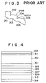
- FIG. 1 to 3 The schematic structural views of a conventional APD which has been proposed therein are illustrated in Figs. 1 to 3.
- Fig. 1 is a cross-sectional structural view of a conventional APD.
- the I-type band gap graded semiconductor layers 201, 203, 205, 207 and 209, consisting of five layers, acting as the carrier multiplication layer are sandwiched between a P-type semiconductor layer 211 and an N-type semiconductor layer 215, with an electrode 213 being in ohmic contact with the P-type semiconductor layer 211 and an electrode 214 being in ohmic contact with the N-type semiconductor layer 215.
- Fig. 2 is an energy band structural diagram when the conventional APD is placed in the operating condition by applying a strong electric field thereto.
- the energy discontinuity of the hetero junctions 202, 204, 206 at which the band gap will steeply step back promotes the ionization, ionization selectively takes place in the neighborhood of the step backs, thereby multiplying carriers.
- Such a structure is adopted because it can reduce fluctuation on the sites where ionization takes place, and thus reduce fluctuation contained in the multiplication process. Accordingly, it is possible to realize a low noise APD, which is applicable to the optical communication system, with less excessive noises and an improved signal-to-noise.
- the conventional APD as above described is effective as a discrete light receiving element for the optical communication which can operate by the application of a strong electric field, but if the conventional APD is used more widely in an application range including photoelectric conversion devices for use with a video camera, a scanner, etc., for performing storage operation, the following problems have often occured.
- the present invention is to resolve the above-mentioned problems, and its objective is to provide a photoelectric conversion device effective in the extensive range of applications, wherein even when a low voltage is applied, it has a high multiplication factor and an excellent response speed, is useful in the industrial field, and can be laminated onto a circuit existing semiconductor substrate, by eliminating the spike and notch at the hetero junctions.
- a photoelectric conversion device comprising a light absorbing layer and a carrier multiplication layer made of non-single crystal material, said carrier multiplication layer comprised of a plurality of layers with the forbidden band width varied continuously, wherein the difference between the Fermi level and the vacuum energy level of said carrier multiplication layer in the neighborhood of a hetero junction is substantially constant.
- Fig. 1 is a cross-sectional structural view for explaining an example of a conventional APD.
- Fig. 2 is a typical energy band structural diagram when the conventional APD is placed in the operating condition by applying a strong electric field thereto.
- Fig. 3 is a typical energy band structural diagram at the step band hetero junctions of carrier multiplication layer when the storage operation is performed with the conventional APD.
- Fig. 4 is a schematic cross-sectional structural view showing the structure of an embodiment of a photoelectric conversion device according to the present invention.
- Fig. 5 is a typical energy band diagram of an embodiment of a photoelectric conversion device according to the present invention when a high electric field is applied.
- Fig. 6 is a typical energy band diagram of an embodiment of a photoelectric conversion device according to the present invention when a low electric field is applied.
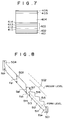
- Fig. 7 is a schematic cross-sectional view showing an embodiment of a photoelectric conversion device according to the present invention.
- Fig. 8 is a typical energy band diagram when a strong electric field is applied to this photoelectric conversion device.
- Fig. 9 is a typical energy band diagram when a weak electric field is applied to this photoelectric conversion device.
- Fig. 10 is a schematic cross-sectional view around a light receiving portion in another embodiment of the present invention.
- Fig. 11 is a one-pixel equivalent circuit diagram of another embodiment of the present invention.
- Fig. 12 is an equivalent circuit diagram of the whole device in another embodiment of the present invention.
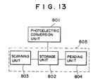
- Fig. 13 is a block diagram for explaining one constitutional example of a photoelectric conversion device to which the present invention is applicable.
- Fig. 4 is a schematic cross-sectional view showing one embodiment of the structure of a photoelectric conversion device according to the present invention, wherein a light absorbing layer 310 and a plurality of forbidden band width graded layers 301, 303, 305, 307 and 309 acting as the carrier multiplication layer are sandwiched between a P-type Semiconductor layer 311 and an N-type semiconductor layer 315 which are charge injection blocking layers, with the P-type semiconductor layer 311 being electrically connected to an electrode 313, and the N-type semiconductor layer 315 being electrically connected to an electrode 314.
- the carrier injection blocking layers may be Schottky joined to adjacent semiconductor layers.
- the forbidden band width graded layers were shown in the case of five layers, but not limitative thereto, it is necessary that they consist of one or two layers or more.
- Fig. 5 is a typical energy band diagram of a photoelectric conversion device of the present invention when a high electric field is applied thereto
- Fig. 6 is a typical energy band diagram of the photoelectric conversion device of the present invention when a low electric field is applied.
- a multiplication principle relying on the avalanche effect is apparently similar to a conventional one as proposed by F. Capasso et al., except that the photoelectric conversion device of the present invention operates as follows.
- the light absorbing layer and the carrier multiplication layer are made of non-single crystalline semiconductor material, and by doping impurities into the carrier multiplication layer, the difference between the Fermi level and the vacuum energy level of the carrier multiplication layer, particularly in the neighborhood of hetero junction is made substantially constant, so that any spike and notch of the hetero junction can be eliminated, whereby it is possible to realize a photoelectric conversion device which has high multiplication factors and excellent response speeds, is effective in the industrial field, and can be laminated on the circuit existing semiconductor substrate, without degrading any performance under the storage operation.
- Fig. 7 is a schematic cross-sectional view showing the structure of one embodiment of a photoelectric conversion device according to the present invention.
- 401 is a Cr electrode
- 402 is a charge injection blocking layer made of an N-type a-Si 1-x Ge x :H having a thickness of about 500 ⁇ for blocking injection of holes
- 403 is a carrier multiplication layer for making carrier multiplication in which the forbidden band width is changed by changing the composition from a-Si 1-x Ge x :H to a-Si 1-y C y :H
- 404 is a light absorbing layer made of a-Si:H having a thickness of about 1 ⁇ m for absorbing the light and producing carriers
- 405 is a charge injection blocking layer made of a P-type a-Si 1-y' C y' :H having a thickness of about 100 ⁇ for blocking injection of electrons
- 406 is a transparent electrode principally made of indium oxide.
- the Cr electrode 401 was created by EB vapor deposition, the transparent electrode 406 was created by sputtering, and the charge injection blocking layer 405, the light absorbing layer 404, the carrier multiplication layer 403 and the charge injection blocking layer 402 were created by plasma CVD.
- Source gases used for creating the amorphous layer were SiH4, GeH4, PH3, H2 for the charge injection blocking layer 402, SiH4, GeH4, CH4, B2H6, H2 for the charge multiplication layer 403, SiH4, H2 for the light absorbing layer 404, and SiH4, CH4, B2H6, H2 for the charge injection blocking layer 405.
- the carrier multiplication layer 403 is comprised of four layers of forbidden band width and Fermi level varying layers 411, 412, 413, 414 having a thickness of 200 ⁇ which were formed by changing continuously the gas flow rates of CH4, GeH4, B2H6 among the source gases of the carrier multiplication layer 403.
- a forbidden band width varying region of the carrier multiplication layer was created by first starting with the formation of a maximum forbidden band width layer from the gases of SiH4, H2, CH4, B2H6, gradually decreasing the flow of CH4 to zero, and then gradually increasing the flow of GeH4 to reach the maximum forbidden band width layer. Also, at this time, the flow of B2H6 is changed in such a way as to gradually decrease from the maximum forbidden band width layer to reach zero in the minimum forbidden band width layer.
- Fig. 8 is an energy band diagram when a strong electric field is applied to the photoelectric conversion device
- Fig. 9 is an energy band diagram when a weak electric field is applied to the photoelectric conversion device.
- Figs. 8 and 9 show that the forbidden band width of an N-type a-Si 1-x Ge x :H layer 501 is Eg4, the minimum forbidden band width of the carrier multiplication layer consisting of four layers of forbidden band width varying layers 511, 512, 513, 514 with the composition changed from a-Si 1-x Ge x :H to a-Si 1-y C y :H is Eg2, the maximum forbidden band width is Eg3, the forbidden band width of a-Si:H layer 503 is Eg1, and the forbidden band width of P-type a-Si 1-y' C y' :H layer 504 is Eg0. Also, it is shown that 515, 516 and 517 are step back hetero junctions.
- the forbidden band width Eg1 of the a-Si:H layer 503 created herein is as large as sbout 1.72 eV.
- the composition ratio y' of C in the a-Si 1-y' C y' :H layer 504 is about 0.2, with its forbidden band width of about 2.2 eV.
- the composition ratio y of the layer a-Si 1-y C y providing the maximum forbidden band width in the forbidden band width varying layers 511, 512, 513, 514 is about 0.5, with its forbidden band width of about 2.9 eV.
- composition ratios x of Ge in the a-Si 1-x Ge x :H layer 501 and the layer a-Si 1-x Ge x :H providing the minimum forbidden band width in the forbidden band width varying layers 511, 512, 513, 514 are both about 0.4, with the forbidden band widths Eg4 and Eg2 being both about 1.4 eV.
- the B density of the forbidden band width varying layer is maximum at the maximum forbidden band width layer, gradually decreasing therefrom to reach zero at the minimum forbidden band width layer.
- the Fermi level of the forbidden band width varying layers 511, 512, 513, 514 is located about 0.4 eV below from the center of the forbidden band in the maximum forbidden band width layer, gradually changing therefrom, and located at the center of the forbidden band in the minimum forbidden band width layer.
- the Fermi level in the neighborhood of the step back hetero junction is substantially constant in a range of about 0.1 eV wide from the vacuum level.
- the multiplication factor of the photoelectric conversion device in this embodiment was substantially constant, or about 10 times, when a bias of 10 V to 20 V was applied. Excessive noise produced with the multiplication was as low as about 1.05. Also, the dark current was as low as about 1 nA/cm2 or less. The response speed was as fast as that of a pin-type photoelectric conversion device without carrier multiplication layer.
- the step back hetero junction was steep, but the same effects can be obtained as well in a range within the mean free path of electron, even if the junction is gentle. Even if the junction is gentler, the step back hetero junction may be satisfied in a range of bringing about the desired action.
- the thickness of composition varying layer is about 200 ⁇ , but may be in a range of thickness in which carriers can transit without recombination. It should be noted that a thinner layer is more preferable because the applied bias can be lowered. Also, in this embodiment, the thickness of the light absorbing layer is about 1 ⁇ m, but may be in a range of thickness in which the incident light does not penetrate through the light receiving layer to reach the carrier multiplication layer, this thickness being determined depending on the incident light absorbing coefficient.
- SiH4, B2H6, PH3, CH4, GeH4 were used in this embodiment, but instead of SiH4, the chain silane compounds such as SiF4, Si2H6, Si2F6, Si3H8, SiH3F, Si2F2, and the cyclic silane compounds such as Si4H8, Si5H10, Si6H12 can be used; instead of B2H6, the gases including III-group atoms such as B, Al, In, Ti can be used; instead of PH3, the gases including V-group atoms such as P, As, Sb, Bi can be used, including the carbon compounds such as CH4, CH2F2, C2H6, C2H4, C2H2, Si(CH3)4, SiH(CH3)3, the nitrogen compounds such as N2, NH3, H2NNH2, HN3NH4N3, F3N, F4N, and the oxygen compounds such as O2, CO2, NO, NO2, N2O, O3, N2O3, N2O4, NO3; and instead of GeH4,
- composition ratio x or y in the forbidden band width varying layer is preferably in a range from 0 to about 0.6 in order to decrease the local level.
- the ECR plasma method is effective for the fabrication of amorphous layer.
- the amorphous layer was used for the semiconductor layer, but the non-single crystal such as polycrystal may be used.
- light is incident from the P layer side of the charge injection blocking layer to effect the multiplication operation with electrons, but it will be appreciated that light may be incident from the N side of the charge injection blocking layer to effect the multiplication operation with holes in such as way as to form steep step back hetero junction on the valence band side of the carrier multiplication layer by exchanging the P layer and the N layer of the charge injection blocking layer.
- the forbidden band width of charge injection blocking layer and the doping amount may be adjusted so that the injection of minority carriers from the electrode be suppressed and the transit property of majority carriers not be prevented.
- Fig. 10 is a schematic cross-sectional view around the light receiving portion in this example of the present invention
- Fig. 11 is an equivalent circuit diagram of one pixel
- Fig. 12 is an equivalent circuit and block diagram of the whole device.
- an N ⁇ layer 702 useful as the collector region is formed on an N-type silicone substrate 701 by epitaxial growth, and a P base region 703 and an N+ emitter region 704 are further formed within it, so that a bipolar transistor is constituted.
- the P base region 703 is separated apart from adjacent pixels, and a gate electrode 706 is formed, with an oxide film 705 interposed between adjacent P base regions extending in the horizontal direction. Accordingly, a P channel MOS transistor is constituted with adjacent P base regions 703 made respectively as the source and drain regions.
- the gate electrode 706 also acts as a capacitor for controlling the voltage of the P base region 703. Further, after forming an insulation layer 707, an emitter electrode 708 and a base electrode 708' are formed.
- a carrier multiplication layer 713 is constituted by forming the forbidden band width varying layers 721, 722, 723, 724 of a-Si 1-x Ge x :H to a-Si 1-y C y :H. Then, a light absorbing layer a-Si:H layer 714, a P-type a-Si 1-y' C y' :H layer 715 and a transparent electrode 716 for applying the bias are formed.
- a collector electrode 717 is disposed in ohmic contact therewith on the back side of the substrate 701.
- an equivalent circuit of one pixel is as shown in Fig. 11, in which a P channel MOS transistor 732, a capacitor 733 and a photoelectric conversion device 734 as in the previous example are connected to the base of a bipolar transistor 731, and a terminal 735 for supplying the voltage to the base, a terminal 736 for driving the P channel MOS transistor 732 and the capacitor, an electrode 737 for supplying the voltage to the transparent electrode, an emitter electrode 738 and a collector electrode 739 are provided.
- Fig. 12 is a circuit configuration diagram in which one-pixel cells 740 as shown in Fig. 11 are arranged in a two dimensional matrix of 3 ⁇ 3.
- a collector electrode 741 of one-pixel cell 740 is provided in each of all pixels, and a sensor electrode 742 is also provided.
- a gate electrode and a capacitor electrode of the PMOS transistor are connected to respective one of the drive lines 743, 743', 743'' for each row leading to a vertical shift register (V. S. R.) 744.
- an emitter electrode is connected to respective one of the vertical lines 746, 746', 746'' for reading signals for each column.
- the vertical lines 746, 746', 746'' are connected respectively to the reset switches 747, 747', 747'' for resetting the charge of the vertical lines and the read switches 750, 750', 750''.
- the gate electrode of the reset switches 747, 747', 747'' are commonly connected to a terminal 748 for applying vertical line reset pulses, and the sources electrode thereof are commonly connected to a terminal 749 for applying the vertical line reset voltage.
- the gate electrode of the read switches 750, 750', 750'' is connected via the lines 751, 751', 751'' to a horizontal shift register (H. S. R.) 752, and the drain electrode thereof is connected via a horizontal read line 753 to an output amplifier 757.
- H. S. R. horizontal shift register
- the horizontal read line 753 is connected to a switch 754 for resetting the charge of the horizontal read line.
- a reset switch 754 is connected to a terminal 755 for applying the horizontal line reset pulse and a terminal 756 for applying the horizontal line reset voltage.
- the output of the amplifier 757 is led out of a terminal 758.
- Figs. 10 to 12 the operation will be described briefly.
- the incident light is absorbed by the light absorbing layer 714 as shown in Fig. 10, and produced carriers are amplified in the multiplication region 713 and stored in the base region 703. If a drive pulse output from the vertical shift register of Fig. 12 appears in the drive line 743, the base voltage will rise up via the capacitor, so that signal charge corresponding to the light quantity, beginning with the pixel on the first row, are passed into the vertical lines 746, 746', 746''.
- the read switches 750, 750', 750'' are controlled in sequence to turn on or off, so that the signal is led out of the output terminal 758 through the amplifier 757.
- the reset switch 754 is turned on while the switches 750, 750', 750'' are turned on in sequence, so that residual charges on the horizontal line 753 are removed.
- the vertical line reset switches 747, 747', 747'' are turned on, so that residual charges on the vertical lines 746, 746', 746'' are removed.
- each PMOS transistor on the first row is turned on, so that base residual charges of each pixel are removed and the initialization is effected. Then, a drive pulse output from the vertical shift register 744 appears on the drive line 743', so that signal charges at the second row are similarly taken out. And then signal charges on the third row are similarly taken out.
- FIG. 13 is a block diagram showing a constitution in which the present invention is applied to a photoelectric conversion device of the typical constitution.
- 801 is a photoelectric conversion unit according to the invention, for which a photoelectric conversion device of the present invention, for example, as shown above, can be used.
- the photoelectric conversion unit 801 is connected to a signal output unit 805.
- 802 is a storage unit for storing signal charges produced by the photoelectric conversion unit 801
- 803 is a scanning unit for driving the storage unit 802
- 804 is a reading unit consisting of a circuit for effecting the multiplication and the noise compensation of signal charges transferred by the scanning unit 803.
- the storage unit 802 is necessary to effect storage operation, but may be omitted if the storage operation is not performed.
- the present invention is a photoelectric conversion device comprising a light absorbing layer and a carrier multiplication layer made of non-single crystalline materials, the carrier multiplication layer being comprised of a plurality of layers with the forbidden band width thereof changed continuously, arranged one above the other, wherein by doping impurities into the carrier multiplication layer, the difference between the Fermi level and the vacuum energy level of the carrier multiplication layer, particularly in the neighborhood of hetero junction is substantially constant, so that any spike and notch in the hetero junction are eliminated, whereby the photoelectric conversion device has high multiplication factors and excellent response speeds even under the application of low voltages, and is effective industrially and capable of being laminated onto a circuit existing semiconductor substrate.
- a photoelectric conversion device wherein, in order to realize a photoelectric conversion device with high multiplication factors and excellent response speeds even under the application of low voltage by eliminating spike and notch in the hetero junction, a light absorbing layer (404) and a carrier multiplication layer (403) are made of non-single crystalline materials, said carrier multiplication layer (403) being comprised of a plurality of layers (411 to 414) with the forbidden band width changed continuously, and wherein the difference between the Fermi level and the vacuum energy level of said carrier multiplication layer (403) in the neighborhood of hetero junction is made substantially constant.
Landscapes
- Power Engineering (AREA)
- Engineering & Computer Science (AREA)
- Physics & Mathematics (AREA)
- Electromagnetism (AREA)
- Computer Hardware Design (AREA)
- General Physics & Mathematics (AREA)
- Condensed Matter Physics & Semiconductors (AREA)
- Microelectronics & Electronic Packaging (AREA)
- Crystallography & Structural Chemistry (AREA)
- Chemical & Material Sciences (AREA)
- Light Receiving Elements (AREA)
- Measuring Pulse, Heart Rate, Blood Pressure Or Blood Flow (AREA)
- Solid State Image Pick-Up Elements (AREA)
- Transforming Light Signals Into Electric Signals (AREA)
Applications Claiming Priority (3)
| Application Number | Priority Date | Filing Date | Title |
|---|---|---|---|
| JP15888992 | 1992-05-27 | ||
| JP158889/92 | 1992-05-27 | ||
| JP4158889A JPH05335615A (ja) | 1992-05-27 | 1992-05-27 | 光電変換装置 |
Publications (2)
| Publication Number | Publication Date |
|---|---|
| EP0571944A1 true EP0571944A1 (fr) | 1993-12-01 |
| EP0571944B1 EP0571944B1 (fr) | 1999-12-01 |
Family
ID=15681599
Family Applications (1)
| Application Number | Title | Priority Date | Filing Date |
|---|---|---|---|
| EP93108415A Expired - Lifetime EP0571944B1 (fr) | 1992-05-27 | 1993-05-25 | Dispositif de conversion photoélectrique |
Country Status (5)
| Country | Link |
|---|---|
| US (1) | US5869851A (fr) |
| EP (1) | EP0571944B1 (fr) |
| JP (1) | JPH05335615A (fr) |
| AT (1) | ATE187278T1 (fr) |
| DE (1) | DE69327130T2 (fr) |
Cited By (2)
| Publication number | Priority date | Publication date | Assignee | Title |
|---|---|---|---|---|
| US6696710B2 (en) | 2001-02-27 | 2004-02-24 | Agilent Technologies, Inc. | Heterojunction bipolar transistor (HBT) having an improved emitter-base junction |
| EP3029745A4 (fr) * | 2013-08-28 | 2016-08-24 | Huawei Tech Co Ltd | Photodiode à avalanche |
Families Citing this family (7)
| Publication number | Priority date | Publication date | Assignee | Title |
|---|---|---|---|---|
| DE60042666D1 (de) * | 1999-01-14 | 2009-09-17 | Panasonic Corp | Halbleiterbauelement und Verfahren zu dessen Herstellung |
| JP2001135851A (ja) * | 1999-11-05 | 2001-05-18 | Minolta Co Ltd | 光電変換素子および固体撮像装置 |
| US6369426B2 (en) * | 2000-04-27 | 2002-04-09 | Infineon Technologies North America Corp. | Transistor with integrated photodetector for conductivity modulation |
| US7453129B2 (en) | 2002-12-18 | 2008-11-18 | Noble Peak Vision Corp. | Image sensor comprising isolated germanium photodetectors integrated with a silicon substrate and silicon circuitry |
| KR100604865B1 (ko) * | 2004-06-08 | 2006-07-26 | 삼성전자주식회사 | 신호 대 잡음비가 향상된 aps 셀 |
| KR101435517B1 (ko) * | 2008-05-28 | 2014-08-29 | 삼성전자주식회사 | 광검출 분자를 이용한 이미지 센서 및 그 구동방법 |
| KR101428147B1 (ko) * | 2011-12-18 | 2014-08-08 | 엘지이노텍 주식회사 | 태양광 발전장치 및 이의 제조방법 |
Citations (4)
| Publication number | Priority date | Publication date | Assignee | Title |
|---|---|---|---|---|
| EP0087299A2 (fr) * | 1982-02-23 | 1983-08-31 | Western Electric Company, Incorporated | Photodétecteur à avalanche multicouche |
| EP0437633A1 (fr) * | 1989-08-04 | 1991-07-24 | Canon Kabushiki Kaisha | Convertisseur photoelectrique |
| EP0444963A2 (fr) * | 1990-03-02 | 1991-09-04 | Canon Kabushiki Kaisha | Dispositif photoélectrique à transfert |
| WO1992004734A1 (fr) * | 1990-09-07 | 1992-03-19 | Georgia Tech Research Corporation | Imageur a transport de charge acoustique |
Family Cites Families (7)
| Publication number | Priority date | Publication date | Assignee | Title |
|---|---|---|---|---|
| JPH0760888B2 (ja) * | 1985-06-12 | 1995-06-28 | キヤノン株式会社 | 光電変換装置 |
| JPH0654957B2 (ja) * | 1985-11-13 | 1994-07-20 | キヤノン株式会社 | 光電変換装置 |
| JPH0644619B2 (ja) * | 1986-07-17 | 1994-06-08 | キヤノン株式会社 | 光電変換装置 |
| US4866293A (en) * | 1986-12-09 | 1989-09-12 | Canon Kabushiki Kaisha | Photoelectric converting apparatus to prevent the outflow of excess carriers |
| EP0277016B1 (fr) * | 1987-01-29 | 1998-04-15 | Canon Kabushiki Kaisha | Dispositif de conversion photovoltaique |
| JPH0234977A (ja) * | 1988-07-25 | 1990-02-05 | Matsushita Electric Ind Co Ltd | 光検出器及びその製造法 |
| US5260560A (en) * | 1990-03-02 | 1993-11-09 | Canon Kabushiki Kaisha | Photoelectric transfer device |
-
1992
- 1992-05-27 JP JP4158889A patent/JPH05335615A/ja active Pending
-
1993
- 1993-05-25 EP EP93108415A patent/EP0571944B1/fr not_active Expired - Lifetime
- 1993-05-25 AT AT93108415T patent/ATE187278T1/de active
- 1993-05-25 DE DE69327130T patent/DE69327130T2/de not_active Expired - Fee Related
-
1997
- 1997-06-03 US US08/867,924 patent/US5869851A/en not_active Expired - Fee Related
Patent Citations (4)
| Publication number | Priority date | Publication date | Assignee | Title |
|---|---|---|---|---|
| EP0087299A2 (fr) * | 1982-02-23 | 1983-08-31 | Western Electric Company, Incorporated | Photodétecteur à avalanche multicouche |
| EP0437633A1 (fr) * | 1989-08-04 | 1991-07-24 | Canon Kabushiki Kaisha | Convertisseur photoelectrique |
| EP0444963A2 (fr) * | 1990-03-02 | 1991-09-04 | Canon Kabushiki Kaisha | Dispositif photoélectrique à transfert |
| WO1992004734A1 (fr) * | 1990-09-07 | 1992-03-19 | Georgia Tech Research Corporation | Imageur a transport de charge acoustique |
Non-Patent Citations (1)
| Title |
|---|
| PATENT ABSTRACTS OF JAPAN vol. 14, no. 187 (E-917)16 April 1990 & JP-A-2 034 977 ( MATSUSHITA ELECTRIC IND CO LTD ) 5 February 1990 * |
Cited By (2)
| Publication number | Priority date | Publication date | Assignee | Title |
|---|---|---|---|---|
| US6696710B2 (en) | 2001-02-27 | 2004-02-24 | Agilent Technologies, Inc. | Heterojunction bipolar transistor (HBT) having an improved emitter-base junction |
| EP3029745A4 (fr) * | 2013-08-28 | 2016-08-24 | Huawei Tech Co Ltd | Photodiode à avalanche |
Also Published As
| Publication number | Publication date |
|---|---|
| JPH05335615A (ja) | 1993-12-17 |
| US5869851A (en) | 1999-02-09 |
| DE69327130T2 (de) | 2000-06-21 |
| DE69327130D1 (de) | 2000-01-05 |
| ATE187278T1 (de) | 1999-12-15 |
| EP0571944B1 (fr) | 1999-12-01 |
Similar Documents
| Publication | Publication Date | Title |
|---|---|---|
| US5686734A (en) | Thin film semiconductor device and photoelectric conversion device using the thin film semiconductor device | |
| US5723877A (en) | Photoelectric conversion apparatus | |
| US5985689A (en) | Method of fabricating photoelectric conversion device having at least one step-back layer | |
| EP0638941A2 (fr) | Phototransistor avec une structure de base à puits quantique | |
| CA2050435C (fr) | Dispositif photosensible | |
| US5869851A (en) | Photoelectric conversion device with graded band gap and carrier concentration | |
| EP0283699B1 (fr) | Dispositif de conversion photo-électrique | |
| GB2372630A (en) | Epitaxial passivation of group 2-6 infrared photodetectors | |
| EP0444963B1 (fr) | Dispositif photoélectrique à transfert | |
| EP0437633B1 (fr) | Convertisseur photoelectrique | |
| US4453184A (en) | Solid state imaging device | |
| CA2059176C (fr) | Dispositif de conversion photoelectrique et appareil de traitement d'images utilisant ce dispositif | |
| EP0495414B1 (fr) | Dispositif de conversion photo-électrique et appareil de traitement d'image utilisant ce dispositif | |
| US5767560A (en) | Photoelectric conversion device and method of driving the same | |
| US5260560A (en) | Photoelectric transfer device | |
| JP2977164B2 (ja) | 光電変換装置 | |
| US5747864A (en) | Light receiving element and a method of fabricating the same | |
| JP2977165B2 (ja) | 光電変換装置 | |
| JPH03253082A (ja) | 光電変換装置 | |
| de Cesare et al. | Modeling and realization of a high-gain homojunction a-Si: H bulk barrier phototransistor | |
| JPH04282873A (ja) | 光電変換装置 | |
| JP2959681B2 (ja) | 光電変換装置 | |
| Su et al. | A comparison between different structures of amorphous silicon image sensors | |
| JPH04370720A (ja) | 光電変換装置の駆動方法 | |
| JPH05291610A (ja) | 光電変換素子 |
Legal Events
| Date | Code | Title | Description |
|---|---|---|---|
| PUAI | Public reference made under article 153(3) epc to a published international application that has entered the european phase |
Free format text: ORIGINAL CODE: 0009012 |
|
| AK | Designated contracting states |
Kind code of ref document: A1 Designated state(s): AT BE CH DE DK ES FR GB GR IE IT LI LU MC NL PT SE |
|
| 17P | Request for examination filed |
Effective date: 19940418 |
|
| 17Q | First examination report despatched |
Effective date: 19950718 |
|
| GRAG | Despatch of communication of intention to grant |
Free format text: ORIGINAL CODE: EPIDOS AGRA |
|
| GRAG | Despatch of communication of intention to grant |
Free format text: ORIGINAL CODE: EPIDOS AGRA |
|
| GRAH | Despatch of communication of intention to grant a patent |
Free format text: ORIGINAL CODE: EPIDOS IGRA |
|
| GRAH | Despatch of communication of intention to grant a patent |
Free format text: ORIGINAL CODE: EPIDOS IGRA |
|
| GRAA | (expected) grant |
Free format text: ORIGINAL CODE: 0009210 |
|
| AK | Designated contracting states |
Kind code of ref document: B1 Designated state(s): AT BE CH DE DK ES FR GB GR IE IT LI LU MC NL PT SE |
|
| PG25 | Lapsed in a contracting state [announced via postgrant information from national office to epo] |
Ref country code: SE Free format text: THE PATENT HAS BEEN ANNULLED BY A DECISION OF A NATIONAL AUTHORITY Effective date: 19991201 Ref country code: NL Free format text: LAPSE BECAUSE OF FAILURE TO SUBMIT A TRANSLATION OF THE DESCRIPTION OR TO PAY THE FEE WITHIN THE PRESCRIBED TIME-LIMIT Effective date: 19991201 Ref country code: LI Free format text: LAPSE BECAUSE OF FAILURE TO SUBMIT A TRANSLATION OF THE DESCRIPTION OR TO PAY THE FEE WITHIN THE PRESCRIBED TIME-LIMIT Effective date: 19991201 Ref country code: IT Free format text: LAPSE BECAUSE OF FAILURE TO SUBMIT A TRANSLATION OF THE DESCRIPTION OR TO PAY THE FEE WITHIN THE PRE;WARNING: LAPSES OF ITALIAN PATENTS WITH EFFECTIVE DATE BEFORE 2007 MAY HAVE OCCURRED AT ANY TIME BEFORE 2007. THE CORRECT EFFECTIVE DATE MAY BE DIFFERENT FROM THE ONE RECORDED.SCRIBED TIME-LIMIT Effective date: 19991201 Ref country code: GR Free format text: LAPSE BECAUSE OF NON-PAYMENT OF DUE FEES Effective date: 19991201 Ref country code: ES Free format text: THE PATENT HAS BEEN ANNULLED BY A DECISION OF A NATIONAL AUTHORITY Effective date: 19991201 Ref country code: CH Free format text: LAPSE BECAUSE OF FAILURE TO SUBMIT A TRANSLATION OF THE DESCRIPTION OR TO PAY THE FEE WITHIN THE PRESCRIBED TIME-LIMIT Effective date: 19991201 Ref country code: BE Free format text: LAPSE BECAUSE OF FAILURE TO SUBMIT A TRANSLATION OF THE DESCRIPTION OR TO PAY THE FEE WITHIN THE PRESCRIBED TIME-LIMIT Effective date: 19991201 Ref country code: AT Free format text: LAPSE BECAUSE OF FAILURE TO SUBMIT A TRANSLATION OF THE DESCRIPTION OR TO PAY THE FEE WITHIN THE PRESCRIBED TIME-LIMIT Effective date: 19991201 |
|
| REF | Corresponds to: |
Ref document number: 187278 Country of ref document: AT Date of ref document: 19991215 Kind code of ref document: T |
|
| REG | Reference to a national code |
Ref country code: CH Ref legal event code: EP |
|
| REF | Corresponds to: |
Ref document number: 69327130 Country of ref document: DE Date of ref document: 20000105 |
|
| REG | Reference to a national code |
Ref country code: IE Ref legal event code: FG4D |
|
| PG25 | Lapsed in a contracting state [announced via postgrant information from national office to epo] |
Ref country code: DK Free format text: LAPSE BECAUSE OF FAILURE TO SUBMIT A TRANSLATION OF THE DESCRIPTION OR TO PAY THE FEE WITHIN THE PRESCRIBED TIME-LIMIT Effective date: 20000301 |
|
| PG25 | Lapsed in a contracting state [announced via postgrant information from national office to epo] |
Ref country code: PT Free format text: LAPSE BECAUSE OF FAILURE TO SUBMIT A TRANSLATION OF THE DESCRIPTION OR TO PAY THE FEE WITHIN THE PRESCRIBED TIME-LIMIT Effective date: 20000302 |
|
| ET | Fr: translation filed | ||
| NLV1 | Nl: lapsed or annulled due to failure to fulfill the requirements of art. 29p and 29m of the patents act | ||
| PG25 | Lapsed in a contracting state [announced via postgrant information from national office to epo] |
Ref country code: LU Free format text: LAPSE BECAUSE OF NON-PAYMENT OF DUE FEES Effective date: 20000525 Ref country code: IE Free format text: LAPSE BECAUSE OF NON-PAYMENT OF DUE FEES Effective date: 20000525 |
|
| REG | Reference to a national code |
Ref country code: CH Ref legal event code: PL |
|
| PG25 | Lapsed in a contracting state [announced via postgrant information from national office to epo] |
Ref country code: MC Free format text: LAPSE BECAUSE OF NON-PAYMENT OF DUE FEES Effective date: 20000710 |
|
| PLBE | No opposition filed within time limit |
Free format text: ORIGINAL CODE: 0009261 |
|
| STAA | Information on the status of an ep patent application or granted ep patent |
Free format text: STATUS: NO OPPOSITION FILED WITHIN TIME LIMIT |
|
| 26N | No opposition filed | ||
| REG | Reference to a national code |
Ref country code: IE Ref legal event code: MM4A |
|
| REG | Reference to a national code |
Ref country code: GB Ref legal event code: IF02 |
|
| PGFP | Annual fee paid to national office [announced via postgrant information from national office to epo] |
Ref country code: FR Payment date: 20060515 Year of fee payment: 14 |
|
| PGFP | Annual fee paid to national office [announced via postgrant information from national office to epo] |
Ref country code: DE Payment date: 20060518 Year of fee payment: 14 |
|
| PGFP | Annual fee paid to national office [announced via postgrant information from national office to epo] |
Ref country code: GB Payment date: 20060524 Year of fee payment: 14 |
|
| GBPC | Gb: european patent ceased through non-payment of renewal fee |
Effective date: 20070525 |
|
| REG | Reference to a national code |
Ref country code: FR Ref legal event code: ST Effective date: 20080131 |
|
| PG25 | Lapsed in a contracting state [announced via postgrant information from national office to epo] |
Ref country code: DE Free format text: LAPSE BECAUSE OF NON-PAYMENT OF DUE FEES Effective date: 20071201 |
|
| PG25 | Lapsed in a contracting state [announced via postgrant information from national office to epo] |
Ref country code: GB Free format text: LAPSE BECAUSE OF NON-PAYMENT OF DUE FEES Effective date: 20070525 |
|
| PG25 | Lapsed in a contracting state [announced via postgrant information from national office to epo] |
Ref country code: FR Free format text: LAPSE BECAUSE OF NON-PAYMENT OF DUE FEES Effective date: 20070531 |