EP0568942A1 - Sende-Empfangumschalter für TDMA-Funkgeräte - Google Patents
Sende-Empfangumschalter für TDMA-Funkgeräte Download PDFInfo
- Publication number
- EP0568942A1 EP0568942A1 EP93107091A EP93107091A EP0568942A1 EP 0568942 A1 EP0568942 A1 EP 0568942A1 EP 93107091 A EP93107091 A EP 93107091A EP 93107091 A EP93107091 A EP 93107091A EP 0568942 A1 EP0568942 A1 EP 0568942A1
- Authority
- EP
- European Patent Office
- Prior art keywords
- switch
- tdma
- antenna
- receiver
- transmitter
- Prior art date
- Legal status (The legal status is an assumption and is not a legal conclusion. Google has not performed a legal analysis and makes no representation as to the accuracy of the status listed.)
- Granted
Links
Images
Classifications
-
- H—ELECTRICITY
- H04—ELECTRIC COMMUNICATION TECHNIQUE
- H04B—TRANSMISSION
- H04B1/00—Details of transmission systems, not covered by a single one of groups H04B3/00 - H04B13/00; Details of transmission systems not characterised by the medium used for transmission
- H04B1/38—Transceivers, i.e. devices in which transmitter and receiver form a structural unit and in which at least one part is used for functions of transmitting and receiving
- H04B1/40—Circuits
- H04B1/44—Transmit/receive switching
Definitions
- the invention relates to a transceiver switch for TDMA radio devices with an antenna switchover to two antennas.
- an antenna switch is provided on the antenna side of a radio, which consists, for example, of a relay or a semiconductor switch.
- the transmit and receive signals are either separated from each other by a duplex filter or by individual filters in the transmit and receive path, which are alternately connected to the antenna switch using a transmit / receive switch.
- the through attenuations of the duplex filter and the antenna switch or the individual filter and the series connection of transmit / receive switch and antenna switch add up. Overall, this leads to a significant deterioration in receiver sensitivity and output power, or to an increase in battery power consumption.
- the invention has for its object to provide a switching device of simple construction to solve the problem described above.
- a double TDMA switch located in the connection path of the transmitter and the receiver to the two antennas, controlled by a TDMA switching signal, by the antenna switch provided for antenna switching corresponding to the applied TDMA switching signal when the switch is in the relevant position alternately a connection is switched from the transmitter or receiver of the radio to the antenna that is switched on.
- the fast TDMA switch as a transceiver is designed so that it is able to switch to two different antennas without increasing the number of damping switching elements. Since current only flows in the case of transmission or reception, the circuit operates in a very energy-saving manner.
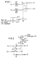
- a filter BP1 is arranged in the signal path of the transmitter and a filter BP2 is arranged in the signal path of the receiver.
- Transmitter and receiver can be connected to antennas 1 and 2 via a double TDMA switch S1.
- the TDMA switch S1 is controlled by a TDMA signal via a relay R.
- a further switch S2 is arranged in the path of the TDMA signal, which is designed as a two-way switch and effects the connection of antenna 1 or antenna 2 in its two switching positions.
- an inverting switching element I is switched on, which causes the TDMA signal to be reversed, for example +5 V when transmitting and 0 V when receiving.
- This switch position is shown in Figure 1.
- the TDMA signal is fed directly to relay R.
- the radio works on the antenna 1.
- the TDMA signal of +5 V when transmitting in the inverting element I receives the state 0 V, so that the TDMA switch S1 remains in the rest position shown and the transmitter is connected to the antenna 1.
- the TDMA signal of 0 V for the reception case is converted to a positive signal at the inverting element I, the TDMA switch S1 reaches its working position via the relay R, so that the receiver is connected to the antenna 1.
- the TDMA signal goes directly to the relay R.
- the TDMA signal of +5 V triggers the relay R and thus switches the TDMA switch S1 from the shown rest position to the Working position, whereby the transmitter is switched on to antenna 2.
- the TDMA signal has the value 0 V, ie the TDMA switch S1 remains in the rest position, so that the receiver is connected to the antenna 2.
- FIG. 2 shows a schematic illustration of a semiconductor switch as a transmit / receive changeover switch, in which a diode D1, D2, D3, D4 is switched on in the connection path between the transmitter and receiver and the antennas 1 and 2.
- a diode D1, D2, D3, D4 is switched on in the connection path between the transmitter and receiver and the antennas 1 and 2.
- These can be, for example, PIN diodes that are switched via a TDMA switching signal of ⁇ 5 V.
- the diode D1 is inserted in the connection path from the transmitter to the antenna 1 and the diode D2 in the connection path from the receiver to the antenna 1.
- Diode D3 is in the connection path from the receiver to the antenna 2, diode D4 in the connection path from the transmitter to the antenna 2.
- the TDMA switching signal is supplied via an ohmic voltage divider R1, R2 and R3, R4, the connection points of the resistors R1 and R2 as well R3 and R4 are each connected to a connection contact of the antenna switch S2 which is connected to ground with its center contact.
- the second connection of the resistor R2 is connected to the connection point of the two diodes D1 and D2 and the antenna 1, the second connection of the resistor R4 to the connection point of the diodes D3 and D4 and the antenna 2.
- this transceiver switch is as follows: in the case shown in FIG. 2, in which the transmitter and receiver are connected to antenna 1, the diode D1 is switched through when a TDMA switching signal of +5 V is applied, so that the transmitter is switched on the antenna 1 is present. A TDMA switching signal of -5 V is applied for the reception case. As a result, the diode D2 is switched through and the receiver is connected to the antenna 1.
- the diode D4 When switching the antenna switch S2 (dashed line), the diode D4 is switched through when the TDMA switching signal of +5 V is applied, so that the transmitter is connected to the antenna 2. When received, a TDMA switching signal of -5 V is applied, causing the diode D3 is switched through and thus the receiver is connected to antenna 2. Since the diode current only has to flow in the case of transmission and reception, this circuit is very energy-efficient.
Landscapes
- Engineering & Computer Science (AREA)
- Computer Networks & Wireless Communication (AREA)
- Signal Processing (AREA)
- Transceivers (AREA)
- Radio Relay Systems (AREA)
Abstract
Description
- Die Erfindung bezieht sich auf einen Sende-Empfangsumschalter für TDMA-Funkgeräte mit einer Antennenumschaltung auf zwei Antennen.
- Auf der Antennenseite eines Funkgerätes ist zur Umschaltung von einer internen auf eine externe Antenne ein Antennenumschalter vorgesehen, der beispielsweise aus einem Relais oder einem Halbleiterschalter besteht. Das Sende- und Empfangssignal werden entweder über ein Duplexfilter voneinander getrennt oder über Einzelfilter im Sende- und Empfangsweg, die über einen Sende-Empfangsumschalter wechselweise an den Antennenumschalter angeschaltet werden. Entsprechend der Ausgestaltung addieren sich dabei die Durchgangsdämpfungen des Duplexfilters und des Antennenumschalters oder der Einzelfilter und der Serienschaltung aus Sende-Empfangsumschalter und Antennenumschalter. Insgesamt führt dies zu einer deutlichen Verschlechterung der Empfängerempfindlichkeit und der Ausgangsleistung bzw. zu einer Erhöhung der Batteriestromaufnahme.
- Zur Behebung dieser Probleme kann man beispielsweise verlustarme, aber voluminöse Filter und Relais verwenden oder die Empfängerempfindlichkeit und Sendeausgangsleistung den erhöhten Durchgangsdämpfungen anpassen. Dies bedeutet jedoch eine Erhöhung des Aufwandes, die bei Handfunkgeräten nicht mehr vertretbar ist.
- Der Erfindung liegt die Aufgabe zugrunde, zur Lösung des vorstehend geschilderten Problems eine Schalteinrichtung einfachen Aufbaus zu schaffen.
- Diese Aufgabe wird gemäß der Erfindung gelöst durch einen im Verbindungsweg des Senders und des Empfängers zu den beiden Antennen liegenden, von einem TDMA-Schaltsignal angesteuerten doppelten TDMA-Schalter, durch den bei der betreffenden Schalterstellung eines zur Antennenumschaltung vorgesehenen Antennenumschalters entsprechend dem anliegenden TDMA-Schaltsignal wechselweise eine Verbindung vom Sender bzw. Empfänger des Funkgerätes zu der jeweils angeschalteten Antenne geschaltet wird.
- Der schnelle TDMA-Schalter als Sende-Empfangsumschalter ist dabei so ausgelegt, daß er ohne Erhöhung der Zahl dämpfender Schaltelemente in der Lage ist, auf zwei verschiedene Antennen umzuschalten. Da nur im Sende- bzw. Empfangsfall Strom fließt, arbeitet die Schaltung sehr stromsparend.
- Vorteilhafte Ausgestaltungen und Weiterbildungen des Erfindungsgegenstandes sind in den Unteransprüchen angegeben.
- Nachstehehend wird die Erfindung anhand von in der Zeichnung dargestellten Ausführungsbeispielen näher erläutert.
- Es zeigen:
- Figur 1
- eine Ausführungsform mit einem doppelten TDMA-Schalter (schneller Halbleiterschalter) in schematischer Darstellung und
- Figur 2
- eine schematische Darstellung des Halbleiterschalters mit PIN-Dioden.
- Beim Ausführungsbeispiel nach Figur 1 ist im Signalweg des Senders ein Filter BP1 und im Signalweg des Empfängers ein Filter BP2 angeordnet. Sender und Empfänger sind über einen doppelten TDMA-Schalter S1 an die Antennen 1 und 2 anschaltbar. Es handelt sich hierbei um eine schematische Darstellung des Schalters, um den Schaltvorgang zu erläutern. Der TDMA-Schalter S1 wird von einem TDMA-Signal über ein Relais R angesteuert. Dabei ist im Weg des TDMA-Signals ein weiterer Schalter S2 angeordnet, der als Wechselschalter ausgebildet ist und in seinen beiden Schaltstellungen den Anschluß der Antenne 1 oder der Antenne 2 bewirkt. Im Verbindungsweg der Schalterstellung für Antenne 1 ist ein invertierendes Schaltelement I eingeschaltet, das eine Umkehrung des TDMA-Signals, z.B. +5 V beim Senden und 0 V beim Empfangen, bewirkt. Diese Schalterstellung ist in Figur 1 gezeigt. In der zweiten Schalterstellung für die Anschaltung von Antenne 2 wird das TDMA-Signal dem Relais R direkt zugeführt.
- Nachstehend wird die Funktionsweise der Schaltung näher erläutert: In der gezeigten Stellung des Antennenumschalters S2 arbeitet das Funkgerät auf der Antenne 1. Dies bedeutet, daß das TDMA-Signal von +5 V beim Senden im invertierenden Element I den Zustand 0 V erhält, so daß der TDMA-Schalter S1 in der gezeigten Ruhestellung verbleibt und der Sender an der Antenne 1 liegt. Das TDMA-Signal von 0 V für den Empfangsfall wird am invertierenden Element I in ein positives Signal umgewandelt, der TDMA-Schalter S1 gelangt über das Relais R in seine Arbeitsstellung, so daß der Empfänger mit der Antenne 1 verbunden wird.
- In der Schalterstellung des Antennenumschalters S2 für Antenne 2 gelangt das TDMA-Signal direkt zum Relais R. Im Sendefall bewirkt das TDMA-Signal von +5 V ein Ansprechen des Relais R und damit eine Umschaltung des TDMA-Schalters S1 von der gezeigten Ruhestellung in die Arbeitsstellung, wodurch der Sender an die Antenne 2 angeschaltet wird. Im Empfangsfall weist das TDMA-Signal den Wert 0 V auf, d.h. der TDMA-Schalter S1 verbleibt in der Ruhestellung, so daß der Empfänger mit der Antenne 2 verbunden ist.
- Figur 2 zeigt in schematischer Darstellung einen Halbleiterschalter als Sende-Empfangs-Umschalter, bei dem im Verbindungsweg von Sender und Empfänger zu den Antennen 1 und 2 jeweils eine Diode D1, D2, D3, D4 eingeschaltet ist. Dies können beispielsweise PIN-Dioden sein, die Über ein TDMA-Schaltsignal von ±5 V geschaltet werden. Dabei ist die Diode D1 im Verbindungsweg vom Sender zur Antenne 1 und die Diode D2 im Verbindungsweg vom Empfänger zur Antenne 1 eingefügt. Diode D3 liegt im Verbindungsweg vom Empfänger zur Antenne 2, Diode D4 im Verbindungsweg vom Sender zur Antenne 2. Die Zuführung des TDMA-Schaltsignals erfolgt über jeweils einen ohmschen Spannungsteiler R1, R2 und R3, R4, wobei die Verbindungspunkte der Widerstände R1 und R2 sowie R3 und R4 mit jeweils einem Anschlußkontakt des mit seinem Mittenkontakt auf Masse liegenden Antennenumschalters S2 verbunden sind. Der zweite Anschluß des Widerstandes R2 ist mit dem Verbindungspunkt der beiden Dioden D1 und D2 und der Antenne 1 verbunden, der zweite Anschluß des Widerstandes R4 mit dem Verbindungspunkt der Dioden D3 und D4 und der Antenne 2.
- Die Funktion dieses Sende-Empfangs-Umschalters ist folgende: Für den in Figur 2 dargestellten Fall, daß Sender und Empfänger an Antenne 1 geschaltet sind, wird beim Anlegen eines TDMA-Schaltsignals von +5 V die Diode D1 durchgeschaltet, so daß der Sender an der Antenne 1 anliegt. Für den Empfangsfall wird ein TDMA-Schaltsignal von -5 V angelegt. Dadurch wird die Diode D2 durchgeschaltet und der Empfänger liegt an der Antenne 1.
- Bei Umschaltung des Antennenumschalters S2 (strichlierte Darstellung) wird beim Anlegen des TDMA-Schaltsignals von +5 V die Diode D4 durchgeschaltet, so daß der Sender an der Antenne 2 anliegt. Im Empfangsfall wird ein TDMA-Schaltsignal von -5 V angelegt, wodurch die Diode D3 durchgeschaltet wird und damit der Empfänger auf die Antenne 2 geschaltet ist. Da der Diodenstrom nur im Sende- und Empfangsfall zu fließen braucht, ist diese Schaltung sehr stromsparend.
Claims (5)
- Sende-Empfangsumschalter für TDMA-Funkgeräte mit einer Antennenumschaltung auf zwei Antennen, gekennzeichnet durch einen im Verbindungsweg des Senders und des Empfängers zu den beiden Antennen liegenden, von einem TDMA-Schaltsignal angesteuerten doppelten TDMA-Schalter, durch den bei der betreffenden Schalterstellung eines zur Antennenumschaltung vorgesehenen Antennenwahlumschalters entsprechend dem anliegenden TDMA-Schaltsignal wechselweise eine Verbindung vom Sender und Empfänger des Funkgerätes zu der jeweils angeschalteten Antenne geschaltet wird.
- Sende-Empfangsumschalter nach Anspruch 1, dadurch gekennzeichnet, daß bei dem verwendeten doppelten TDMA-Schalter jeweils nur ein Einfügungsdämpfung verursachendes Schaltelement zwischen der angewählten Antenne und dem Sendeausgang oder Empfängereingang liegt.
- Sende-Empfangsumschalter nach Anspruch 1 oder 2, dadurch gekennzeichnet, daß der doppelte TDMA-Schalter als schneller Halbleiterschalter realisiert ist mit Halbleiterelementen im Verbindungsweg von Sender und Empfänger zur der jeweiligen Antenne, die bei Ansteuerung mit dem betreffenden für Sende- oder Empfangsbetrieb vorgesehenen Schaltsignal durchgeschaltet werden.
- Sende-Empfangsumschalter nach Anspruch 3, dadurch gekennzeichnet, daß die Halbleiterelemente aus PIN-Dioden bestehen.
- Sende-Empfangsumschalter nach Anspruch 1 oder 2, dadurch gekennzeichnet, daß der doppelte TDMA-Schalter im Verbindungsweg zwischen Sender bzw. Empfänger des Funkgerätes und den Antennen aus den Schaltkontakten eines Relais besteht, das über einen im Zuführungsweg der Schaltsignale liegenden Antennenwahlschalter von den Schaltsignalen in der Weise angesteuert wird, daß die Schaltsignale in der einen Schalterstellung des Antennenwahlschalters dem Relais direkt und in der anderen Schalterstellung über einen Inverter zugeführt wird.
Applications Claiming Priority (2)
| Application Number | Priority Date | Filing Date | Title |
|---|---|---|---|
| DE4214859 | 1992-05-05 | ||
| DE4214859 | 1992-05-05 |
Publications (2)
| Publication Number | Publication Date |
|---|---|
| EP0568942A1 true EP0568942A1 (de) | 1993-11-10 |
| EP0568942B1 EP0568942B1 (de) | 1998-03-04 |
Family
ID=6458233
Family Applications (1)
| Application Number | Title | Priority Date | Filing Date |
|---|---|---|---|
| EP93107091A Expired - Lifetime EP0568942B1 (de) | 1992-05-05 | 1993-04-30 | Sende-Empfangsumschalter für TDMA-Funkgeräte |
Country Status (4)
| Country | Link |
|---|---|
| EP (1) | EP0568942B1 (de) |
| AT (1) | ATE163819T1 (de) |
| DE (1) | DE59308193D1 (de) |
| ES (1) | ES2112928T3 (de) |
Citations (2)
| Publication number | Priority date | Publication date | Assignee | Title |
|---|---|---|---|---|
| EP0355973A2 (de) * | 1988-08-16 | 1990-02-28 | Nokia Mobile Phones Ltd. | Digitales mobiles Fernsprechgerät |
| WO1992000634A1 (en) * | 1990-06-22 | 1992-01-09 | Motorola, Inc. | Full duplex/half duplex power radio |
-
1993
- 1993-04-30 EP EP93107091A patent/EP0568942B1/de not_active Expired - Lifetime
- 1993-04-30 AT AT93107091T patent/ATE163819T1/de not_active IP Right Cessation
- 1993-04-30 DE DE59308193T patent/DE59308193D1/de not_active Expired - Fee Related
- 1993-04-30 ES ES93107091T patent/ES2112928T3/es not_active Expired - Lifetime
Patent Citations (2)
| Publication number | Priority date | Publication date | Assignee | Title |
|---|---|---|---|---|
| EP0355973A2 (de) * | 1988-08-16 | 1990-02-28 | Nokia Mobile Phones Ltd. | Digitales mobiles Fernsprechgerät |
| WO1992000634A1 (en) * | 1990-06-22 | 1992-01-09 | Motorola, Inc. | Full duplex/half duplex power radio |
Non-Patent Citations (1)
| Title |
|---|
| PATENT ABSTRACTS OF JAPAN vol. 015, no. 514 (E-1150)27. Dezember 1991 & JP-A-32 26 124 ( MITSUBISHI ELECTRIC ) * |
Also Published As
| Publication number | Publication date |
|---|---|
| ATE163819T1 (de) | 1998-03-15 |
| DE59308193D1 (de) | 1998-04-09 |
| EP0568942B1 (de) | 1998-03-04 |
| ES2112928T3 (es) | 1998-04-16 |
Similar Documents
| Publication | Publication Date | Title |
|---|---|---|
| DE68907613T2 (de) | Anordnung mit bandsperrfiltern. | |
| DE2709096C2 (de) | Antennenumschalteinrichtung | |
| DE2047001B2 (de) | Anordnungen für die Übertragung von Daten innerhalb einer Datenverarbeitungsanlage | |
| EP0069979A2 (de) | Antennenanpasseinrichtung | |
| EP0234453B1 (de) | Schaltungsanordnung zur seriellen Datenübertragung zwischen mehreren Teilnehmerstellen | |
| EP0235648A1 (de) | Schaltungsanordnung zur seriellen Datenübertragung zwischen mehreren Teilnehmerstellen | |
| DE3642378C2 (de) | ||
| EP0208984B1 (de) | Verfahren zur automatischen Impedanzanpassung eines Senders an eine Antenne | |
| EP0568942A1 (de) | Sende-Empfangumschalter für TDMA-Funkgeräte | |
| EP1065105B1 (de) | Schaltungsanordnung zur Signalkopplung zwischen Schaltungsteilen mit voneinander getrennten Versorgungsleitungen | |
| DE2456630C3 (de) | Fernsteueranlage | |
| EP0521253A2 (de) | Verfahren zur bidirektionalen Datenübertragung | |
| EP0184210B1 (de) | Datenübertragungseinrichtung | |
| EP0419712A1 (de) | Entkopplungsglied für ein Kommunikations-Bus-System | |
| DE2138576C3 (de) | Umsetzerschaltung zum Übertragen von Gleichstrom-Telegraphiezeichen | |
| DE68927894T2 (de) | Filterwirkung aufweisende mittel durch antennendiversity | |
| DE3444362A1 (de) | Station mit einem datensender | |
| DE2714417A1 (de) | Schaltungsanordnung zur uebertragung von signalen in beiden richtungen ueber signalleitungen in fernmelde-, insbesondere fernsprechanlagen | |
| DE2905301C3 (de) | Sende-Empfangsstation | |
| EP0003755B1 (de) | Schaltungsanordnung zum Empfang von Einfachstrom- und Doppelstrom-Telegrafiezeichen | |
| DE69100502T2 (de) | Verstärker mit Doppelbandausgang. | |
| DE2213459C2 (de) | Schaltungsanordnung fur Mehr frequenzencodezeichenempfänger in Fern melde , insbesondere Fernsprechanlagen mit zusätzlichem Datenverkehr | |
| DE3727165C2 (de) | ||
| DE1117181B (de) | Einrichtung fuer die antennenseitige Umschaltung eines Sende-Empfangs-Geraetes auf ein Reservegeraet | |
| DE4332475A1 (de) | Fahrzeuggerät zur Datenübertragung an eine ortsfeste Bake |
Legal Events
| Date | Code | Title | Description |
|---|---|---|---|
| PUAI | Public reference made under article 153(3) epc to a published international application that has entered the european phase |
Free format text: ORIGINAL CODE: 0009012 |
|
| AK | Designated contracting states |
Kind code of ref document: A1 Designated state(s): AT BE DE DK ES FR GB IT NL SE |
|
| 17P | Request for examination filed |
Effective date: 19940322 |
|
| 17Q | First examination report despatched |
Effective date: 19961122 |
|
| GRAG | Despatch of communication of intention to grant |
Free format text: ORIGINAL CODE: EPIDOS AGRA |
|
| GRAG | Despatch of communication of intention to grant |
Free format text: ORIGINAL CODE: EPIDOS AGRA |
|
| GRAH | Despatch of communication of intention to grant a patent |
Free format text: ORIGINAL CODE: EPIDOS IGRA |
|
| GRAH | Despatch of communication of intention to grant a patent |
Free format text: ORIGINAL CODE: EPIDOS IGRA |
|
| GRAA | (expected) grant |
Free format text: ORIGINAL CODE: 0009210 |
|
| AK | Designated contracting states |
Kind code of ref document: B1 Designated state(s): AT BE DE DK ES FR GB IT NL SE |
|
| REF | Corresponds to: |
Ref document number: 163819 Country of ref document: AT Date of ref document: 19980315 Kind code of ref document: T |
|
| REF | Corresponds to: |
Ref document number: 59308193 Country of ref document: DE Date of ref document: 19980409 |
|
| PGFP | Annual fee paid to national office [announced via postgrant information from national office to epo] |
Ref country code: AT Payment date: 19980416 Year of fee payment: 6 |
|
| REG | Reference to a national code |
Ref country code: ES Ref legal event code: FG2A Ref document number: 2112928 Country of ref document: ES Kind code of ref document: T3 |
|
| PGFP | Annual fee paid to national office [announced via postgrant information from national office to epo] |
Ref country code: NL Payment date: 19980420 Year of fee payment: 6 |
|
| PGFP | Annual fee paid to national office [announced via postgrant information from national office to epo] |
Ref country code: BE Payment date: 19980422 Year of fee payment: 6 |
|
| PGFP | Annual fee paid to national office [announced via postgrant information from national office to epo] |
Ref country code: SE Payment date: 19980423 Year of fee payment: 6 |
|
| ET | Fr: translation filed | ||
| ITF | It: translation for a ep patent filed | ||
| GBT | Gb: translation of ep patent filed (gb section 77(6)(a)/1977) |
Effective date: 19980507 |
|
| PG25 | Lapsed in a contracting state [announced via postgrant information from national office to epo] |
Ref country code: DK Free format text: LAPSE BECAUSE OF FAILURE TO SUBMIT A TRANSLATION OF THE DESCRIPTION OR TO PAY THE FEE WITHIN THE PRESCRIBED TIME-LIMIT Effective date: 19980604 |
|
| PLBE | No opposition filed within time limit |
Free format text: ORIGINAL CODE: 0009261 |
|
| 26N | No opposition filed | ||
| PG25 | Lapsed in a contracting state [announced via postgrant information from national office to epo] |
Ref country code: BE Free format text: LAPSE BECAUSE OF NON-PAYMENT OF DUE FEES Effective date: 19990430 Ref country code: AT Free format text: LAPSE BECAUSE OF NON-PAYMENT OF DUE FEES Effective date: 19990430 |
|
| PG25 | Lapsed in a contracting state [announced via postgrant information from national office to epo] |
Ref country code: SE Free format text: LAPSE BECAUSE OF NON-PAYMENT OF DUE FEES Effective date: 19990501 |
|
| BERE | Be: lapsed |
Owner name: SIEMENS A.G. Effective date: 19990430 |
|
| PG25 | Lapsed in a contracting state [announced via postgrant information from national office to epo] |
Ref country code: NL Free format text: LAPSE BECAUSE OF NON-PAYMENT OF DUE FEES Effective date: 19991101 |
|
| NLV4 | Nl: lapsed or anulled due to non-payment of the annual fee |
Effective date: 19991101 |
|
| EUG | Se: european patent has lapsed |
Ref document number: 93107091.6 |
|
| REG | Reference to a national code |
Ref country code: GB Ref legal event code: IF02 |
|
| PGFP | Annual fee paid to national office [announced via postgrant information from national office to epo] |
Ref country code: IT Payment date: 20060430 Year of fee payment: 14 |
|
| REG | Reference to a national code |
Ref country code: GB Ref legal event code: 732E |
|
| REG | Reference to a national code |
Ref country code: FR Ref legal event code: TP |
|
| PGFP | Annual fee paid to national office [announced via postgrant information from national office to epo] |
Ref country code: DE Payment date: 20070426 Year of fee payment: 15 |
|
| PGFP | Annual fee paid to national office [announced via postgrant information from national office to epo] |
Ref country code: ES Payment date: 20070511 Year of fee payment: 15 |
|
| PGFP | Annual fee paid to national office [announced via postgrant information from national office to epo] |
Ref country code: GB Payment date: 20070525 Year of fee payment: 15 |
|
| PGFP | Annual fee paid to national office [announced via postgrant information from national office to epo] |
Ref country code: FR Payment date: 20070430 Year of fee payment: 15 |
|
| GBPC | Gb: european patent ceased through non-payment of renewal fee |
Effective date: 20080430 |
|
| PG25 | Lapsed in a contracting state [announced via postgrant information from national office to epo] |
Ref country code: DE Free format text: LAPSE BECAUSE OF NON-PAYMENT OF DUE FEES Effective date: 20081101 |
|
| REG | Reference to a national code |
Ref country code: FR Ref legal event code: ST Effective date: 20081231 |
|
| PG25 | Lapsed in a contracting state [announced via postgrant information from national office to epo] |
Ref country code: FR Free format text: LAPSE BECAUSE OF NON-PAYMENT OF DUE FEES Effective date: 20080430 |
|
| REG | Reference to a national code |
Ref country code: ES Ref legal event code: FD2A Effective date: 20080503 |
|
| PG25 | Lapsed in a contracting state [announced via postgrant information from national office to epo] |
Ref country code: GB Free format text: LAPSE BECAUSE OF NON-PAYMENT OF DUE FEES Effective date: 20080430 |
|
| PG25 | Lapsed in a contracting state [announced via postgrant information from national office to epo] |
Ref country code: ES Free format text: LAPSE BECAUSE OF NON-PAYMENT OF DUE FEES Effective date: 20080503 |
|
| PG25 | Lapsed in a contracting state [announced via postgrant information from national office to epo] |
Ref country code: IT Free format text: LAPSE BECAUSE OF NON-PAYMENT OF DUE FEES Effective date: 20070430 |