EP0567104A2 - Circuit for detecting refresh address signals of a semiconductor memory device - Google Patents
Circuit for detecting refresh address signals of a semiconductor memory device Download PDFInfo
- Publication number
- EP0567104A2 EP0567104A2 EP93106502A EP93106502A EP0567104A2 EP 0567104 A2 EP0567104 A2 EP 0567104A2 EP 93106502 A EP93106502 A EP 93106502A EP 93106502 A EP93106502 A EP 93106502A EP 0567104 A2 EP0567104 A2 EP 0567104A2
- Authority
- EP
- European Patent Office
- Prior art keywords
- refresh address
- refresh
- address signals
- comparators
- sub
- Prior art date
- Legal status (The legal status is an assumption and is not a legal conclusion. Google has not performed a legal analysis and makes no representation as to the accuracy of the status listed.)
- Granted
Links
Images

Classifications
-
- G—PHYSICS
- G11—INFORMATION STORAGE
- G11C—STATIC STORES
- G11C29/00—Checking stores for correct operation ; Subsequent repair; Testing stores during standby or offline operation
- G11C29/02—Detection or location of defective auxiliary circuits, e.g. defective refresh counters
-
- G—PHYSICS
- G11—INFORMATION STORAGE
- G11C—STATIC STORES
- G11C11/00—Digital stores characterised by the use of particular electric or magnetic storage elements; Storage elements therefor
- G11C11/21—Digital stores characterised by the use of particular electric or magnetic storage elements; Storage elements therefor using electric elements
- G11C11/34—Digital stores characterised by the use of particular electric or magnetic storage elements; Storage elements therefor using electric elements using semiconductor devices
- G11C11/40—Digital stores characterised by the use of particular electric or magnetic storage elements; Storage elements therefor using electric elements using semiconductor devices using transistors
- G11C11/401—Digital stores characterised by the use of particular electric or magnetic storage elements; Storage elements therefor using electric elements using semiconductor devices using transistors forming cells needing refreshing or charge regeneration, i.e. dynamic cells
- G11C11/406—Management or control of the refreshing or charge-regeneration cycles
Landscapes
- Engineering & Computer Science (AREA)
- Microelectronics & Electronic Packaging (AREA)
- Computer Hardware Design (AREA)
- Dram (AREA)
- For Increasing The Reliability Of Semiconductor Memories (AREA)
Abstract
Description
- The present invention relates to a semiconductor memory device and particularly to a self-refresh address test circuit of a semiconductor memory device which has a self-refresh function with using an internal self-refresh address.
- As a semiconductor memory device having a self-refresh function, a dynamic random access memory (referred to as DRAM hereinafter) has been known. The DRAM comprises a memory cell array consisted of a plurality of memory cells which are coupled with a plurality of word lines and a plurality of bit lines arranged in matrix, and peripheral circuits for controlling read and write operation of data into and from the memory cell selected by a combination of the word line and bit line. Each of the memory cells in the DRAM comprises a single MOSFET (metal-oxide-semiconductor field effect transistor) and a single capacitor. Data written into a memory cell is charged in the single capacitor of the memory cell, and the logic state of the data is determined by the amount of the charge stored in the single capacitor. For protecting the data stored in the single capacitor of a memory cell from degradation thereof due to a current leakage with lapse of time, a refresh function is provided to the memory cell in order to restore an original data level of the memory cell. In recent DRAMs, the refresh operation is automatically performed with a predetermined period, repeatedly, and made by itself to all the memory cells embedded in the DRAM. Such is called as a self-refresh operation wherein addresses for selecting memory cells in sequent are generated in the DRAM without using external addresses as is in normal operation.
- One of conventional self-refresh technologies in a DRAM has been disclosed in Japanese Patent Publication No. 61 57079 (issued on 1986), as the title of "a dynamic semiconductor memory device". In the Japanese paper, a self-refresh operation mode is enabled after a predetermined lapse time from when CAS-before-RAS refresh mode (referred to as "CBR mode" hereinafter) is initiated. If a row address strobe signal


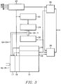
- Referring to Fig.1 showing functional constitution of a DRAM employing the conventional self-refresh scheme and Fig.2 illustrating the operation timing of Fig.1, for performing a self-refresh operation, the conventional DRAM comprises a
refresh control circuit 22 generating a refresh clock ΦRFSH according to a CBR informing signal made by acontrol signal generator 20 which receives a row address strobe signal


refresh address counter 24 generating a plurality of internal refresh address signals Q₀-Qn-1 response to the refresh clock ΦRFSH. Referring to Fig.2 which illustrates the refresh clock ΦRFSH and the internal refresh address signals Q₀-Qn-1, the refresh clock ΦRFSH is generated from therefresh control circuit 22 by an oscillator (not shown) therein, reponing to initiation of the CBR informing signal. Once the refresh clock ΦRFSH is applied to therefresh address counter 24, a plurality of internal refresh address signals Q₀-Qn-1 are generated from therefresh address counter 24 and applied to alow decoder 12 and acolumn decoder 16, for the purpose of being used for selecting memory cells in amemory cell array 10 in regular sequence. With using the internal refresh address signals Q₀-Qn-1 a self-refresh operation is made up to the memory cells in thememory cell array 10. - However, It is impossible for the conventional self-refresh circuit as shown in Fig.1 to detect a condition about whether all the internal refresh address signals necessary to accomplishing the self-refresh operation have been completely generated, thereby, as well as to verify its cycle time as a substantial value. Since, if a semiconductor memory device products has the self-refresh function, an accurate self-refresh cycle time should be joined with its own standardization, absence of the self-refresh cycle time detecting or verifying means detracts such a memory products from reliability of itself.
- Accordingly, it is an object of the present invention to provide a refresh address test circuit of a semiconductor memory device having a self-refresh function.
- It is another object of the present invention to provide a refresh address test circuit which is capable of verifying a self-refresh cycle time.
- It is still another object of the present invention to provide a semiconductor memory device in which an information about whether internal refresh address signals for one self-refresh cycle are completely generated can be detected.
- In order to achieve the objects of the present invention described above, the semiconductor memory circuit according to the present invention comprises a memory cell array with a plurality of memory cells, a selection means for selecting one of the memory cells, an input and output means for storing and retrieving data into and from the memory cells, a refresh control circuit for generating a refresh clock, a refresh address counter for generating a plurality of refresh address signals response to the refresh clock and apply the refresh address signals to the selection means, and a refresh address test circuit for detecting whether the refresh address signals has been completely generated or not. The refresh address test circuit comprises a plurality of the address test paths, each including a first sub-path with an initial logic level of the refresh address signal and a second sub-path of refresh address signal, a plurality of comparators, each receiving the initial logic level of the refresh address signal from the first sub-path and a present logic level of the refresh address signal from the second sub-path, a test output circuit for receiving the output signals generated from the plurality of comparators.
- It is preferred that the first sub-path comprises latch means for holding the initial logic levels of the refresh address signals, switch means for transferring the initial logic levels of the refresh address signals to the comparators. It is also preferred that the comparators is activated at least before the refresh address signals are commonly on same logic level.
- These objects and other objects, features, aspects and advantages of the present invention will become more apparent from the following detailed description of the present invention when taken in conjunction with the accompanying drawings.
- Fig. 1 is a functional block diagram of a conventional semiconductor memory device employing a self-refresh function.
- Fig. 2 is a timing chart diagram of Fig. 1, showing a refresh clock and internal refresh address signals.
- Fig. 3 is a functional block diagram of a semiconductor memory device comprising a refresh address test circuit according to the present invention.
- Fig. 4 shows an embodiment of the refresh address test circuit of Fig,3, according to the present invention.
- Fig. 5 shows an embodiment of a comparator provided to the refresh address test circuit of Fig.4, according to the present invention.
- Fig. 6 is a timing chart diagram of Fig.3, when the semiconductor memory device according to the present invention is performing a self-refresh operation with the refresh address test circuit of Fig.4.
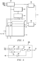
- Prior to description about an embodiment according to the present invention hereinafter, note that functional block elements of Fig.3 as same as those of Fig.1 are marked with numerals as is in Fig.1. Now, referring to Fig. 3, other components in Fig.3 is as same as those of Fig.1 but a refresh
address test circuit 30 which receives a plurality of internal refresh address signals Q₀-Qn-1, generated from arefresh address counter 24 and applies an address test signal to adata output buffer 28. A CBR informing signal made from acontrol signal generator 20 from which an input/output control signal is also generated is applied to arefresh control circuit 22, anaddress buffer 14, arow decoder 12 and asense amplifier 18. Theaddress buffer 14 turns its input to the internal refresh address from the external address A₀-An-1 when the semiconductor memory device of Fig.3 is in a self-refresh operation mode. Thedata output buffer 28 makes the address test signal be generated out of the semiconductor memory device. Detail circuit of the refreshaddress test circuit 30 is shown in Fig.4. - Referring to Fig.4, the refresh
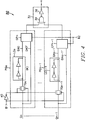
address test circuit 30 according to the present invention comprises a plurality of address test paths PQ₀-PQn-1 receiving the plurality of the internal refresh address signals Q₀-Qn-1 applied from therefresh address counter 24, atest output circuit 32 receiving all signals passed through the address test paths PQ₀-PQn-1 and generating the address test signal which detects whether all the refresh addresses Q₀-Qn-1 for one self-refresh cycle have been completely generated. - All the plurality of the address test paths PQ₀-PQn-1 are constructed with same manner. Representatively, a first address test path PQ₀ is consisted of a first sub-path DA₀, a second sub-path DA₀', a first comparator CP₀ receiving signals on the first and second sub-paths DA₀ and DA₀' and being controlled by a comparing control signal Φ2. The first sub-path DA₀ receives a first refresh address signal Q₀ and is coupled to one input terminal of the first comparator CP₀, including a first transmission gate TG₀ transferring the first refresh address signal Q₀ by means of a transmission control clock Φ1, a first latch circuit LC₀ coupled between the first transmission gate TG₀ and the one input terminal of the first comparator CP₀. The second sub-path DA₀' directly applies the first refresh address signal Q₀ to the other input terminal of the first comparator CP₀. Also in other address test paths such as second address test path PQ₁ through n'th address test path PQn-1 each of them is constructed as is in the first address test path PQ₀. For example in a case of anyone address test path PQi, the address test path PQi is consisted of a first sub-path DAi, a second sub-path DAi', an i'th comparator CPi receiving signals on the first and second sub-paths DAi and DAi' and being controlled by the comparing control clock Φ2; the first sub-path DAi receives an i'th refresh address signal Qi and is coupled to one input terminal of the i'th comparator CPi, including an i'th transmission gate TGi transferring the i'th refresh address signal Qi by means of the transmission control clock Φ1 and an i'th latch circuit LCi coupled between the i'th transmission gate TGi and the one input terminal of the i'th comparator CPi; the second sub-path DAi' directly applies the i'th refresh address Qi to the other input terminal of the i'th comparator CPi.
- The
test output circuit 32 is made of aNAND gate 34 receiving all output signals generated from the plurality of the comparators CP₀, CP₁,..., CPn-1 and aninverter 36 coupled to an output terminal of theNAND gate 34 to convert the output signal of theNAND gate 36 to the address test signal. - A logic circuit of the comparator employed in the address test path, as an embodiment according to the present invention, is disclosed in Fig.5. Referring to Fig.5, the i'th comparator CPi (any one of the first comparator CP₀ through the n'th comparator CPn-1 is consisted of a
NAND gate 48 and afirst NOR gate 52 those input terminals are commonly coupled to the first and second sub-paths DAi and DAi', aninverter 50 inverting an output signal of theNAND gate 48, asecond NOR gate 54 receiving output signals from theinverter 50 and thefirst NOR gate 52, aninverter 56 inverting the comparing control clock Φ2, and athird NOR gate 58 receiving the output signals from thesecond NOR gate 54 and theinverter 56 to apply a compared output signal to thetest output circuit 32. - The operation of the refresh address test circuit according to the present invention will now be described in detail with reference to Figs. 3 through 5, and Fig.6 which illustrates figures of the row address strobe signal


control signal generator 20 of Fig.3 at a time t2 to enable a self-refresh operation mode. Then, therefresh control circuit 22 controlled by the CBR informing signal generates the refresh clock ΦRFSH, as shown in Fig.6, by means of an oscillator (not shown), and thereby therefresh address counter 24 generates the plurality of the refresh address signals Q₀-Qn-1. - During the transmission control clock Φ1 retains "low"level, the internal refresh address signals Q₀-Qn-1 are stored into the latch circuits LC₀-LCn-1 on the first sub-paths DA₀-DAn-1, by passing through the transmission gates TG₀-TGn-1. When a first pulse of the refresh clock ΦRFSH changes from "high" level to "low" level in first self-refresh cycle, the transmission control clock Φ1 becomes "high" level. Thereby, the transmission gates TG₀-TGn-1 are closed to be disable so that the stored the initial level of the refresh address signals Q₀-Qn-1 are held on the first sub-paths DA₀-DAn-1 bythe latch circuits LC₀-LCn-l until the self-refresh operation mode has been expired, completely. Subsequently when a second pulse of the refresh clock ΦRFSH goes to "high" level, the comparing control clock Φ2 becomes "high" level to activate the comparators CP₀-CPn-1 which have two input terminals, respectively, the one connected to the output of the latch circuit storing the initial level of the refresh address signal and the other directly receiving the subsequently toggling level of the refresh address signal.
- Referring to Fig.5, in the comparators CPi (any one of the CP₀-CPn-1), the one input terminals of the
NAND gate 48 and thefirst NOR gate 52 are coupled to the initial logic level of the refresh address signal on the first sub-path DAi (any one of the DA₀-DAn-1), and the other input terminals of theNAND gate 48 and thefirst NOR gate 52 are coupled to the subsequently toggling logic level of the refresh address signal on the second sub-path DAi' (any one of the DA₀'-DAn-₁'). If the subsequently toggling logic level of the refresh address signal Qi (any one of the Q₀-Qn-1) is on "low" level at present, assuming that the initial level of the refresh address signal Qi (any one of the Q₀-Qn-1) has been stored in the latch circuit LCi (any one of the LC₀-LCn-1) as "high" level, thesecond NOR gate 54 receives an output signal of "low" level from theinverter 50 which inverts the output level of theNAND gate 48 and also receives an output signal of "low" level from the first NORgate 52. Since the comparing control clock Φ2 retains "high" level at present in order to activate this comparator CPi (any one of the CP₀-CPn-1), thethird NOR gate 58 can generate an output signal of "low" level and apply it to one of the input terminals of thetest output circuit 32 in Fig.4. Because this output signal of "low" level of thethird NOR gate 58 of the comparator CPi, that is, an resultant output signal generated from any one of the address test paths PQ₀-PQn-1, makes the output of thetest output circuit 32 be on "low" level, it represents that all the refresh address signals Q₀-Qn-1 in need of performing one refresh cycle in the self-refresh operation mode have not been completely generated as a whole. - After lapsing aforementioned condition of that each of the refresh address signals Q₀-Qn-1 being generated is toggling from its "high" level to "low" level, or its "low" level to "high" level, all the NAND gates (similar to the NAND gate 48) and the first NOR gates (similar to the first NOR gate 52) of the comparators CP₀-CPn-1 can commonly receive the refresh address signals Q₀-Qn-1 of "high" levels from the second sub-paths DAi' only at the time of that all the refresh address signals Q₀-Qn-1 for the next self-refresh cycle are applied to their own second sub-paths DA₀'-DAn-1ʼ of the address test paths PQ₀-PQn-1, as shown in Fig.6. And then, referring to Fig.5, the
third NOR gate 58 generate an output signal of "high" level, resulting in that the address test signal is generated as "high" level due to all inputs of the HANDgate 34 of thetest output circuit 32 becoming "high" level. Which represents that all the refresh address signals Q₀-Qn-1 in need of performing one self-refresh cycle, that is, the prior self-refresh cycle, in the self-refresh operation mode are completely generated as a whole. Thus, the generating condition of the internal refresh address signals is detected through thedata output buffer 28 and thereby the self-refresh cycle time can be verified. - In the embodiment described above, although the comparing control clock Φ2 is activated at the time of that the second pulse of the refresh clock ΦRFSH goes to its "high" level, it is possible that the activation time of the clock Φ2 can be designed to be enabled just on or before all the refresh address signals has been on their "low" levels in common, as an example on or before the n-1'th pulse of the refresh clock ΦRFSH goes to its "high" level, as shown in Fig.6. This can provide power consumption reducing effect to the semiconductor memory device according to the present invention.
- Moreover, the number of signals to be applied to the comparator, for comparing the initial logic level of the refresh address signal and the present logic level of the refresh address signal, may be obvious to be variable by those skilled in this art.
- As stated above, since the present invention provides a refresh test circuit with means for detecting whether the internal refresh address signals being used for a self-refresh cycle in the self-refresh operation mode has been completely generated or not yet, an accurate self-refresh cycle time can be obtained thereby and the disagreement between the substantial self-refresh cycle time and the standard self-refresh cycle time can be eliminated.
Claims (7)
- A semiconductor memory device having a self-refresh function, comprising:
a memory cell array with a plurality of memory cells;
a selection means for selecting one of said memory cells;
an input and output means for storing and retrieving data into and from said memory cells;
a refresh control circuit for generating a refresh clock;
a refresh address counter for generating a plurality of refresh address signals response to said refresh clock and apply said refresh address signals to said selection means; and
a refresh address test circuit for detecting whether said refresh address signals has been completely generated or not. - A semiconductor memory device as claimed in Claim 1, wherein said refresh address test circuit comprises a plurality of comparators for respectively receiving initial logic levels of said refresh address signals and present logic levels of said refresh address signals, an test output circuit for receiving output signals of said comparators.
- A semiconductor memory device as claimed in Claim 2, wherein said refresh address test circuit comprises latch means for holding said initial logic levels of said refresh address signals, switch means for transferring said initial logic levels of said refresh address signals to said comparators.
- A semiconductor memory device as claimed in Claim 2, wherein each of said comparators is activated at least before said refresh address signals are commonly on same logic level.
- A refresh address test circuit of a semiconductor memory having a self-refresh function with a plurality of internal refresh address signals, comprising:
a plurality of address test paths, each including a first sub-path with an initial logic level of said refresh address signal and a second sub-path of said refresh address signal;
a plurality of comparators, each receiving said initial logic level of said refresh address signal from said first sub-path and a present logic level of said refresh address signal from said second sub-path; and
a test output circuit for receiving the output signals generated from said plurality of comparators. - A refresh address test circuit as claimed in Claim 5, wherein said first sub-path comprises latch means for holding said initial logic levels of said refresh address signals, switch means for transferring said initial logic levels of said refresh address signals to said comparators.
- A refresh address test circuit as claimed in Claim 5, wherein said comparators are activated at least before said refresh address signals are commonly on same logic level.
Applications Claiming Priority (2)
| Application Number | Priority Date | Filing Date | Title |
|---|---|---|---|
| KR1019920006728A KR950009390B1 (en) | 1992-04-22 | 1992-04-22 | Regresh address testing circuit of memory chip |
| KR672892 | 1992-04-22 |
Publications (3)
| Publication Number | Publication Date |
|---|---|
| EP0567104A2 true EP0567104A2 (en) | 1993-10-27 |
| EP0567104A3 EP0567104A3 (en) | 1996-04-17 |
| EP0567104B1 EP0567104B1 (en) | 1998-07-01 |
Family
ID=19332103
Family Applications (1)
| Application Number | Title | Priority Date | Filing Date |
|---|---|---|---|
| EP93106502A Expired - Lifetime EP0567104B1 (en) | 1992-04-22 | 1993-04-21 | Semiconductor memory device having a self-refresh function |
Country Status (7)
| Country | Link |
|---|---|
| US (1) | US5299168A (en) |
| EP (1) | EP0567104B1 (en) |
| JP (1) | JP2843481B2 (en) |
| KR (1) | KR950009390B1 (en) |
| CN (1) | CN1032337C (en) |
| DE (1) | DE69319372T2 (en) |
| TW (1) | TW212251B (en) |
Cited By (1)
| Publication number | Priority date | Publication date | Assignee | Title |
|---|---|---|---|---|
| EP0610862A2 (en) * | 1993-02-10 | 1994-08-17 | Nec Corporation | Dynamic random access memory device with self-refresh cycle time directly measurable at data pin |
Families Citing this family (25)
| Publication number | Priority date | Publication date | Assignee | Title |
|---|---|---|---|---|
| JPH06150646A (en) * | 1992-11-13 | 1994-05-31 | Nec Corp | Semiconductor memory |
| JP3244340B2 (en) * | 1993-05-24 | 2002-01-07 | 三菱電機株式会社 | Synchronous semiconductor memory device |
| US5450364A (en) * | 1994-01-31 | 1995-09-12 | Texas Instruments Incorporated | Method and apparatus for production testing of self-refresh operations and a particular application to synchronous memory devices |
| JP3426693B2 (en) * | 1994-03-07 | 2003-07-14 | 株式会社日立製作所 | Semiconductor storage device |
| KR100372245B1 (en) * | 1995-08-24 | 2004-02-25 | 삼성전자주식회사 | Semiconductor memory device for controlling sequentially word lines |
| JPH09161478A (en) * | 1995-12-12 | 1997-06-20 | Mitsubishi Electric Corp | Semiconductor memory |
| US6392948B1 (en) * | 1996-08-29 | 2002-05-21 | Micron Technology, Inc. | Semiconductor device with self refresh test mode |
| KR100363108B1 (en) * | 1998-12-30 | 2003-02-20 | 주식회사 하이닉스반도체 | Semiconductor memory device and method of adjusting refresh cycle of device |
| JPH11345486A (en) * | 1998-06-01 | 1999-12-14 | Mitsubishi Electric Corp | Dram provided with self-refresh control circuit and system lsi |
| KR100363103B1 (en) * | 1998-10-20 | 2003-02-19 | 주식회사 하이닉스반도체 | Self Refresh Oscillator |
| KR100364128B1 (en) * | 1999-04-08 | 2002-12-11 | 주식회사 하이닉스반도체 | A measuring device of self-refresh oscilation period |
| US6330203B1 (en) | 2000-12-26 | 2001-12-11 | Vanguard International Semiconductor Corporation | Test mode for verification of on-chip generated row addresses |
| JP2002214296A (en) * | 2001-01-16 | 2002-07-31 | Toshiba Corp | Semiconductor device |
| US7184728B2 (en) * | 2002-02-25 | 2007-02-27 | Adc Telecommunications, Inc. | Distributed automatic gain control system |
| DE10228527B3 (en) * | 2002-06-26 | 2004-03-04 | Infineon Technologies Ag | Method for checking the refresh function of an information store |
| KR101130378B1 (en) | 2004-09-09 | 2012-03-27 | 엘지전자 주식회사 | A dish washer and method of controlling the same |
| US7599711B2 (en) | 2006-04-12 | 2009-10-06 | Adc Telecommunications, Inc. | Systems and methods for analog transport of RF voice/data communications |
| DE102006020098A1 (en) * | 2006-04-29 | 2007-10-31 | Infineon Technologies Ag | Dynamic RAM memory circuit, has recreation circuit recreating memory cells based on selection information, and word line decoder selecting one of word lines depending based on address information |
| KR20100128045A (en) | 2009-05-27 | 2010-12-07 | 삼성전자주식회사 | Method of estimating self refresh period of semiconductor memory device |
| KR101752154B1 (en) | 2010-11-02 | 2017-06-30 | 삼성전자주식회사 | Row address control circuit, semiconductor memory device including the same and method of controlling a row address |
| KR101974108B1 (en) * | 2012-07-30 | 2019-08-23 | 삼성전자주식회사 | Refresh address generator, a volatile memory device including the same and method of refreshing volatile memory device |
| KR102194791B1 (en) * | 2013-08-09 | 2020-12-28 | 에스케이하이닉스 주식회사 | Memory, memory including the same and method for operating memory |
| WO2015126828A1 (en) | 2014-02-18 | 2015-08-27 | Commscope Technologiees Llc | Selectively combining uplink signals in distributed antenna systems |
| CN105338131B (en) * | 2015-11-30 | 2019-05-31 | 上海斐讯数据通信技术有限公司 | The test method and system of a kind of Dynamic Host Configuration Protocol server address tankage |
| CN114121074B (en) * | 2020-08-31 | 2023-09-01 | 长鑫存储技术有限公司 | Method and device for testing self-refresh frequency of memory array |
Citations (2)
| Publication number | Priority date | Publication date | Assignee | Title |
|---|---|---|---|---|
| US4672583A (en) * | 1983-06-15 | 1987-06-09 | Nec Corporation | Dynamic random access memory device provided with test circuit for internal refresh circuit |
| US4933908A (en) * | 1988-10-28 | 1990-06-12 | Unisys Corporation | Fault detection in memory refreshing system |
Family Cites Families (4)
| Publication number | Priority date | Publication date | Assignee | Title |
|---|---|---|---|---|
| JPS6035398A (en) * | 1983-08-05 | 1985-02-23 | Nec Corp | Dynamic semiconductor storage device |
| JPS6083294A (en) * | 1983-10-13 | 1985-05-11 | Nec Corp | Automatic refreshing circuit |
| JPH087995B2 (en) * | 1985-08-16 | 1996-01-29 | 富士通株式会社 | Method and apparatus for refreshing dynamic semiconductor memory device |
| JPH0799618B2 (en) * | 1986-03-24 | 1995-10-25 | 日本電気株式会社 | Semiconductor memory test circuit |
-
1992
- 1992-04-22 KR KR1019920006728A patent/KR950009390B1/en not_active IP Right Cessation
-
1993
- 1993-04-20 TW TW082103030A patent/TW212251B/en not_active IP Right Cessation
- 1993-04-21 EP EP93106502A patent/EP0567104B1/en not_active Expired - Lifetime
- 1993-04-21 DE DE69319372T patent/DE69319372T2/en not_active Expired - Lifetime
- 1993-04-22 JP JP5095973A patent/JP2843481B2/en not_active Expired - Fee Related
- 1993-04-22 US US08/050,780 patent/US5299168A/en not_active Expired - Lifetime
- 1993-04-22 CN CN93105919.4A patent/CN1032337C/en not_active Expired - Lifetime
Patent Citations (2)
| Publication number | Priority date | Publication date | Assignee | Title |
|---|---|---|---|---|
| US4672583A (en) * | 1983-06-15 | 1987-06-09 | Nec Corporation | Dynamic random access memory device provided with test circuit for internal refresh circuit |
| US4933908A (en) * | 1988-10-28 | 1990-06-12 | Unisys Corporation | Fault detection in memory refreshing system |
Cited By (2)
| Publication number | Priority date | Publication date | Assignee | Title |
|---|---|---|---|---|
| EP0610862A2 (en) * | 1993-02-10 | 1994-08-17 | Nec Corporation | Dynamic random access memory device with self-refresh cycle time directly measurable at data pin |
| EP0610862A3 (en) * | 1993-02-10 | 1995-12-13 | Nec Corp | Dynamic random access memory device with self-refresh cycle time directly measurable at data pin. |
Also Published As
| Publication number | Publication date |
|---|---|
| CN1078820A (en) | 1993-11-24 |
| DE69319372D1 (en) | 1998-08-06 |
| KR930022383A (en) | 1993-11-24 |
| CN1032337C (en) | 1996-07-17 |
| EP0567104B1 (en) | 1998-07-01 |
| TW212251B (en) | 1993-09-01 |
| US5299168A (en) | 1994-03-29 |
| DE69319372T2 (en) | 1998-10-29 |
| EP0567104A3 (en) | 1996-04-17 |
| JPH06103757A (en) | 1994-04-15 |
| JP2843481B2 (en) | 1999-01-06 |
| KR950009390B1 (en) | 1995-08-21 |
Similar Documents
| Publication | Publication Date | Title |
|---|---|---|
| EP0567104B1 (en) | Semiconductor memory device having a self-refresh function | |
| US8040751B2 (en) | Semiconductor memory device | |
| KR920001758B1 (en) | Pseudo-static memory device having internal self refresh circuit | |
| US5875153A (en) | Internal/external clock option for built-in self test | |
| US6795363B2 (en) | Refresh control method of semiconductor memory device and semiconductor memory device comprising the same control method | |
| EP0895245B1 (en) | Synchronous semiconductor memory device | |
| US6205069B1 (en) | Semiconductor memory device with fast input/output line precharge scheme and method of precharging input/output lines thereof | |
| US7310273B2 (en) | Method for controlling precharge timing of memory device and apparatus thereof | |
| US5708624A (en) | Method and structure for controlling internal operations of a DRAM array | |
| US5790468A (en) | Refresh counter for synchronous dynamic random access memory and method of testing the same | |
| US6563760B2 (en) | Circuit and method for generating internal command signals in a semiconductor memory device | |
| US4807196A (en) | Refresh address counter test control circuit for dynamic random access memory system | |
| US6349072B1 (en) | Random access memory device | |
| KR100462085B1 (en) | Semiconductor memory circuit | |
| US6501701B2 (en) | Semiconductor memory device | |
| US7167948B2 (en) | Semiconductor memory device | |
| KR20000008774A (en) | AUTO-PRECHARGE APPARATUS IN A SYNCHRONOUS DRAM(Dynamic Random Access Memory) | |
| US5515331A (en) | DRAM refresh control circuit | |
| US6108248A (en) | Column address strobe signal generator for synchronous dynamic random access memory | |
| KR100221748B1 (en) | Cache memory device of dram configuration without refresh function | |
| US20080062798A1 (en) | Refresh operation of memory device | |
| JP4386657B2 (en) | Semiconductor memory device | |
| KR19980040799A (en) | Automatic precharge signal generation circuit of semiconductor memory device | |
| US6349066B1 (en) | Semiconductor storage device having a self-refresh circuit for automatically refreshing memory cell | |
| KR100487484B1 (en) | Refresh control circuit of semiconductor memory device |
Legal Events
| Date | Code | Title | Description |
|---|---|---|---|
| PUAI | Public reference made under article 153(3) epc to a published international application that has entered the european phase |
Free format text: ORIGINAL CODE: 0009012 |
|
| AK | Designated contracting states |
Kind code of ref document: A2 Designated state(s): DE FR GB IT |
|
| PUAL | Search report despatched |
Free format text: ORIGINAL CODE: 0009013 |
|
| AK | Designated contracting states |
Kind code of ref document: A3 Designated state(s): DE FR GB IT |
|
| 17P | Request for examination filed |
Effective date: 19960730 |
|
| 17Q | First examination report despatched |
Effective date: 19961217 |
|
| GRAG | Despatch of communication of intention to grant |
Free format text: ORIGINAL CODE: EPIDOS AGRA |
|
| GRAG | Despatch of communication of intention to grant |
Free format text: ORIGINAL CODE: EPIDOS AGRA |
|
| GRAH | Despatch of communication of intention to grant a patent |
Free format text: ORIGINAL CODE: EPIDOS IGRA |
|
| GRAH | Despatch of communication of intention to grant a patent |
Free format text: ORIGINAL CODE: EPIDOS IGRA |
|
| GRAA | (expected) grant |
Free format text: ORIGINAL CODE: 0009210 |
|
| AK | Designated contracting states |
Kind code of ref document: B1 Designated state(s): DE FR GB IT |
|
| REF | Corresponds to: |
Ref document number: 69319372 Country of ref document: DE Date of ref document: 19980806 |
|
| ET | Fr: translation filed | ||
| PLBE | No opposition filed within time limit |
Free format text: ORIGINAL CODE: 0009261 |
|
| STAA | Information on the status of an ep patent application or granted ep patent |
Free format text: STATUS: NO OPPOSITION FILED WITHIN TIME LIMIT |
|
| 26N | No opposition filed | ||
| REG | Reference to a national code |
Ref country code: GB Ref legal event code: IF02 |
|
| PGFP | Annual fee paid to national office [announced via postgrant information from national office to epo] |
Ref country code: IT Payment date: 20080429 Year of fee payment: 16 |
|
| PG25 | Lapsed in a contracting state [announced via postgrant information from national office to epo] |
Ref country code: IT Free format text: LAPSE BECAUSE OF NON-PAYMENT OF DUE FEES Effective date: 20090421 |
|
| PGFP | Annual fee paid to national office [announced via postgrant information from national office to epo] |
Ref country code: GB Payment date: 20120328 Year of fee payment: 20 |
|
| PGFP | Annual fee paid to national office [announced via postgrant information from national office to epo] |
Ref country code: DE Payment date: 20120326 Year of fee payment: 20 |
|
| PGFP | Annual fee paid to national office [announced via postgrant information from national office to epo] |
Ref country code: FR Payment date: 20120522 Year of fee payment: 20 |
|
| REG | Reference to a national code |
Ref country code: DE Ref legal event code: R071 Ref document number: 69319372 Country of ref document: DE |
|
| REG | Reference to a national code |
Ref country code: GB Ref legal event code: PE20 Expiry date: 20130420 |
|
| PG25 | Lapsed in a contracting state [announced via postgrant information from national office to epo] |
Ref country code: GB Free format text: LAPSE BECAUSE OF EXPIRATION OF PROTECTION Effective date: 20130420 Ref country code: DE Free format text: LAPSE BECAUSE OF EXPIRATION OF PROTECTION Effective date: 20130423 |