EP0564868A2 - Appareil de formation d'images - Google Patents
Appareil de formation d'images Download PDFInfo
- Publication number
- EP0564868A2 EP0564868A2 EP93104445A EP93104445A EP0564868A2 EP 0564868 A2 EP0564868 A2 EP 0564868A2 EP 93104445 A EP93104445 A EP 93104445A EP 93104445 A EP93104445 A EP 93104445A EP 0564868 A2 EP0564868 A2 EP 0564868A2
- Authority
- EP
- European Patent Office
- Prior art keywords
- image
- data
- circuit
- pixel
- pulse width
- Prior art date
- Legal status (The legal status is an assumption and is not a legal conclusion. Google has not performed a legal analysis and makes no representation as to the accuracy of the status listed.)
- Withdrawn
Links
Images


Classifications
-
- H—ELECTRICITY
- H04—ELECTRIC COMMUNICATION TECHNIQUE
- H04N—PICTORIAL COMMUNICATION, e.g. TELEVISION
- H04N1/00—Scanning, transmission or reproduction of documents or the like, e.g. facsimile transmission; Details thereof
- H04N1/40—Picture signal circuits
- H04N1/405—Halftoning, i.e. converting the picture signal of a continuous-tone original into a corresponding signal showing only two levels
- H04N1/4055—Halftoning, i.e. converting the picture signal of a continuous-tone original into a corresponding signal showing only two levels producing a clustered dots or a size modulated halftone pattern
- H04N1/4056—Halftoning, i.e. converting the picture signal of a continuous-tone original into a corresponding signal showing only two levels producing a clustered dots or a size modulated halftone pattern the pattern varying in one dimension only, e.g. dash length, pulse width modulation [PWM]
Definitions
- the present invention relates to an image forming apparatus by which images of high quality can be recorded when the distribution of adjacent pixels is reflected by the distribution of density of objective recording pixels.
- the present invention relates to a color image forming apparatus in which color images are formed in the following manner: image data corresponding to one pixel is divided into small pixels of m ⁇ n (width ⁇ length) giving consideration to the adjacent pixel data; the center of gravity of each line is found; a pulse width modulation signal is generated in which the recording position is displaced in accordance with the gravity; and according to the modulation signal, dot-recording composed of small scanning lines, the number of which is "n", is carried out, so that characters and half-tone images are reproduced.
- the recording apparatus is used for a printer and a display device.
- an image on an original is read as image signals by a scanner, and the image signals are subjected to gradation correction, A/D conversion and shading correction to be image density data.
- the image density data are modulated by reference wave signals so that digital images having therein reproduced half-tone images may be obtained.
- an edge portion of the image is read as a half-tone image density due to an aperture of a solid image sensor incorporated in the scanner.
- image density data obtained from the image signals make a latent image on a photoreceptor
- recording pixels corresponding to edges of the latent image are recorded as an average within recording pixels when density is medium. Therefore, sharpness of the image is deteriorated for recording.
- MTF correction methods wherein a differential filter or a Laplacian filter is used for image signals for sharpening images. In these methods, however, only edge portions of an image are sharpened and uniformity of half-tone images is relatively deteriorated.
- the present invention relates to an image forming apparatus, and more particularly relates to a laser beam image forming apparatus in which the laser beam source is driven by a pulse width signal (PWM signal) corresponding to image data so as to reproduce the gradation of the image.
- PWM signal pulse width signal
- a pulse width modulation circuit to generate a pulse width signal having information about gradation includes a D/A converter that converts a digital image signal into an analog signal, a pattern generating circuit that receives an analog signal and generates a predetermined pattern corresponding to the analog signal, and an analog circuit such as a comparator that receives the generated pattern and generates a PWM pulse.
- the pulse width modulation circuit that generates pulse width signals having gradation information includes analog circuit components, which are attached onto the system board as discrete parts. Therefore, the analog circuit components tend to be affected by noises emitted from the circuits disposed around them, so that accuracy can not be maintained stably.
- the present invention relates to an image forming apparatus, and more particularly relates to an image forming apparatus that generates a PWM signal (a pulse width modulation signal) in accordance with the image density data and controls the light emitting time of the light source by the PWM signal so as to reproduce the gradation.
- a PWM signal a pulse width modulation signal
- Fig. 37 is a schematic illustration for explaining a gradation reproduction system in which PWM signals are employed.
- image data (1) in Fig. 37 is temporarily written in the frame memory, and the image data is read out by a reference clock (a reference clock (2) in Fig. 37) corresponding to one pixel.
- the image data that has been read out is converted into an analog signal by a D/A converter (D/A output (3) in Fig. 37 is obtained), and the converted analog signal is compared with a triangular wave (the reference wave (4) in Fig. 37) having a period corresponding to one pixel by a comparator, so that a PWM signal (comparator output (5) in Fig. 37) is generated.
- Light emitting time of the light source (a semiconductor laser and so forth) is controlled by this PWM signal, and an electrostatic latent image is formed on a photoreceptor (latent images (6) A, B, C, D and E formed on the photoreceptor in Fig. 37).
- the first object of the present invention is to provide an image forming apparatus capable of recording an image of high quality using a simple circuit when the resolution of the image determined by a scanner, CG or font data is improved.
- the second object of the present invention is to improve the anti-noise characteristics and accuracy of image processing (PWM pulse generation processing for reproducing the gradation) in which a PWM circuit is used.
- the third object of the present invention is to accomplish compatibility of an improvement in image quality and that in sharpness of an edge portion using a simple structure.
- the first embodiment of the present invention to accomplish the aforementioned object is to provide an image forming apparatus in which a pulse width modulation signal is generated in accordance with the density data of an image and the image is recorded by the pulse width modulation signal, wherein a pulse position of the pulse width modulation signal is displaced corresponding to the density distribution in an objective pixel found from the density of the objective pixel and that of the adjacent pixel.
- the modulation means to generate the pulse width modulation signal and to displace the pulse position corresponding to the density distribution in the objective pixel preferably includes a pulse start and end data generating circuit, one or more programmable delay generators, and a D-type flip-flop.
- a pulse generation means is triggered by an image data transmission clock so that the output level is inverted.
- the image data is inputted into a digital programmable delay generation circuit, so that a pulse having a delay amount corresponding to the image data is generated.
- a pulse generation means is reset by this delay pulse, so that a PWM pulse is generated.
- a changeover means is provided that changes over the maximum delay ranges of a frequency demultiplying circuit, image data averaging circuit and digital programmable delay generation circuit.
- the digital programmable delay circuit converts image data into delay information, and a PWM pulse is generated in accordance with this delay information. Therefore, it is not necessary to provide an analog circuit outside and an analog delay line. Accordingly, the apparatus is hardly subjected to noises emitted by the surrounding circuits. Further, the digital programmable delay circuit composed IC components can be easily operated, and also the number of bits of input and output data can be easily extended, so that it is appropriate to improve the accuracy.
- the path of an image transmission clock and that of image data can be automatically changed over when the printing period is changed, so that processing can be carried out in accordance with an image to be reproduced.
- an image the density level of which fluctuates greatly (that is, with respect to a character image)
- image processing is carried out for each pixel so that a PWM signal corresponding to each pixel is generated and the image is recorded.
- image processing is carried out over not less than 2 pixels so that one PWM signal is generated and the image is recorded.
- an edge portion a portion in which the density is clearly changed
- the recording position is corrected (recording position modulation) with respect to both images.
- the PWM signal is generated using the first reference wave having a period corresponding to each pixel, the second reference wave having a period twice as long as that of the first reference wave, and the third reference wave having a phasic difference of 180° with respect to the phase of the second reference wave, and the level of the image signal that has passed through the A/D converter is compared with that of the reference wave.
- Image reproduction of high resolution is carried out by the image processing for each pixel with respect to an image, the density level of which fluctuates greatly.
- Image reproduction of high gradation is carried out by the image processing over not less than 2 pixels with respect to an image, the density level of which fluctuates little. Further, the sharpness of the edge portion is ensured by carrying out uniform recording position modulation. That is, image reproduction processing is finely conducted, giving consideration to the characteristics of the entire image to be reproduced and the local change of image density. In this way, the image quality can be improved.
- the essential operation is to compare an image signal with a reference wave. Further, one of the second and third reference waves is used for recording position modulation, and also used for processing over not less than 2 pixels when a photographic image is processed, so that the reference wave can be effectively used. In this manner, the structure is simplified.
- Fig. 7 is a perspective view showing the schematic structure of an image forming apparatus of the present example.
- the image forming apparatus 400 is operated in the following manner: After the photoreceptor has been uniformly charged, a dot-shaped electrostatic latent image is formed by a beam of light that has been pulse-width modulated in accordance with the digital image density data sent from the computer or scanner. The electrostatic latent image is reversely developed with toner so that a dot-shaped toner image is formed. The aforementioned charging, exposing and developing processes are repeated to form a color toner image on the photoreceptor. This color toner image is transferred onto a recording paper, and the transferred image is fixed to obtain a color image.
- Image forming apparatus 400 comprises a drum-shaped photoreceptor 401 rotating in the arrowed direction , scorotron charger 402 that gives charges uniformly on the photoreceptor 401, scanning optical system, that is, a laser writing unit 430, developing units 441 - 444 respectively containing yellow toner, magenta toner, cyan toner and black toner, scorotron transferring unit 462, separating unit 463, fixing roller 464, cleaning unit 470 and discharging unit 474.
- scanning optical system that is, a laser writing unit 430, developing units 441 - 444 respectively containing yellow toner, magenta toner, cyan toner and black toner, scorotron transferring unit 462, separating unit 463, fixing roller 464, cleaning unit 470 and discharging unit 474.
- the photoreceptor 401 used in the present example has a high ⁇ characteristic, and an example of its structure is shown in Fig. 9.
- the photoreceptor drum 401 is composed of electrically conductive support 401A, interlayer 401B and light-sensitive layer 401C as shown in Fig. 15.
- the thickness of the light-sensitive layer 401C is about 5 - 100 ⁇ m and preferably is 10 - 50 ⁇ m.
- the photoreceptor 401 consists of conductive support 401A that is made of aluminum and has a diameter of 150 mm on which the interlayer 401B that is made of ethylene-vinyl acetate copolymer and is 0.1 ⁇ m in thickness is formed and 35 ⁇ m thick light-sensitive layer 401C is provided on the interlayer 401B.
- the conductive support 401A a drum made of aluminum, steel or copper and having a diameter of about 150 mm is used.
- a belt-shaped one wherein a metal layer is laminated or evaporated on a sheet of paper or a plastic film, or a metallic belt such as a nickel belt made through a electroforming method may be used.
- the interlayer 401B has a Hall mobility. For that reason, it is preferable that charge-transfer materials of a positive charging type described in Japanese Patent Application Open to Public Inspection No. 44662/1988 suggested previously by the assignee of the present invention are added by an amount of 10% by weight or less.
- the intermediate layer 401B the following resins used for a light-sensitive layer for electrophotography use, for example, are employed in general.
- photoconductive materials consisting of photoconductive pigments and a small amount of charge-transport materials in an amount of not more than 1/5 or preferably of 1/1000 - 1/10 by weight of the photoconductive pigments and antioxidants are dispersed in binder resins to make a light-sensitive layer.
- a photoreceptor with such a high ⁇ it is possible to form a sharp latent image despite an enlarged beam diameter, resulting in effective recording with high resolving power.
- a photoreceptor having its spectral sensitivity on the infrared side and an infrared semiconductor laser are used so that a beam from a scanning optical system may not be shielded by the color toner images.
- Fig. 14 is a graph showing characteristics of a photoreceptor with a high ⁇ .
- V1 represents charging voltage (V)
- V0 represents initial voltage (V) before exposure
- L1 represents an amount of irradiated light ( ⁇ J/cm2) of a laser beam necessary for the initial voltage V0 to decay to 4/5 thereof
- L2 is an amount of irradiated light ( ⁇ J/cm2) of the laser beam necessary to decay to 1/5.
- L2/L1 The preferable range of L2/L1 is as follows. 1.0 ⁇ L2/L1 ⁇ 1.5 The following is for the present example.
- photosensitivity at a position corresponding to the middle point of exposure where the initial voltage (V0) decays to 1/2 thereof on the light decay curve is represented by E1/2
- photosensitivity at a position corresponding to the initial stage of exposure where the initial voltage (V0) decays to 9/10 thereof is represented by E9/10
- a photoconductive semiconductor satisfying the following relations is selected. (E1/2)/(E9/10) ⁇ 2 or (E1/2)/(E9/10) ⁇ 5
- the photosensitivity in this case is defined as an absolute value of an amount of drop of voltage for a small amount of exposure.
- an absolute value of a differential coefficient of a voltage characteristic which means photosensitivity is small when an amount of light is small as shown in Fig. 14, increases sharply as an amount of light increases.
- the light decay curve is almost flat in the initial stage of exposure due to the poor photosensitivity for a certain period as shown in Fig. 14.
- the middle stage and thereafter to the latter stage the light decay curve suddenly falls almost linearly due to the ultra-high sensitivity, which represents ultra-high ⁇ characteristics.
- the photoreceptor 401 practically gains high ⁇ characteristics utilizing an avalanche phenomenon under the high voltage charging at +500 - +2000V. Namely, carriers generated on the surface of photoconductive pigment in the initial stage of exposure are trapped effectively in the surface phase between the pigment and coating resin to inhibit light decay completely which results in a sharp avalanche phenomenon in the middle stage and thereafter.
- the photoreceptor is preferably provided with a high ⁇ characteristic.
- a photoreceptor can be used in which the amount of light is proportional to the amount of potential drop.
- Image signal processing is carried out as follows: An objective one pixel of image density data is composed of small pixels of m ⁇ n. The density data distribution of adjacent pixels including the objective pixel is replaced with the distribution of small pixels of m ⁇ n in one pixel. The data of the objective pixel is multiplied by a constant P, and the obtained result is distributed in accordance with the aforementioned distribution so as to obtain the image density data of small pixels.
- recording position data is found from the density gravity center of each line of small pixels. By the obtained recording position data, the dot writing position of "n" lines is displaced so as to form an image.
- This dot writing position displacing operation will be referred to as recording position modulation, hereinafter.
- the processing in which the objective pixel is converted into image density data of small pixels divided into m ⁇ n will be referred to as resolution enhancement processing (RE processing), hereinafter. Recording of high density can be carried out by this RE processing.
- RE processing resolution enhancement processing
- a high ⁇ photoreceptor is effective for latent image formation conducted by a laser beam writing device.
- the following image forming apparatus is preferably used.
- the image forming apparatus carries out high density pixel recording in accordance with the density distribution data in the objective pixel determined correspondingly to the density data of pixels adjacent to the objective pixel, and in the case where specific density data of the objective pixel is not less than the first threshold value, recording position modulation is carried out in accordance with the determined density distribution. Further, in the case where the specific density data of the objective pixel is not more than the second threshold value, recording position modulation is carried out in accordance with the determined density distribution.
- Fig. 10(a) is a plan view in which: the objective pixel is denoted by m5; objective pixel m5 is divided into 3 ⁇ 3; and adjacent pixels including the objective pixel m5 are denoted by m1 to m9.
- Fig. 10(b) is an enlarged view in which: the objective pixel m5 is divided into small pixels of 3 ⁇ 3; and the small portions are denoted by s1 to s9.
- m1 to m9 and s1 to s9 also denote the density of the portions.
- the term (9 ⁇ m5 ⁇ P ⁇ mi/A) is used in the case where a value obtained when the density of objective pixel m5 is multiplied by P is allotted in accordance with a ratio of the density of the adjacent pixel.
- the term (1 - P) ⁇ m5 is used in the case where the residual density of objective pixel m5 is uniformly allotted to each small pixel. Therefore, the element of blurring is taken into consideration.
- Fig. 11 is a view showing an example in which the objective pixel m5 is divided into 3 ⁇ 3 and P is set at 0.5.
- Fig. 11(a) is a view showing an example of density distribution of the adjacent pixels including the objective pixel m5.
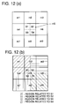
- Figs. 12 and 13 are views showing examples in which the objective pixel m5 is divided into 2 ⁇ 2.
- Fig. 12(a) is a view showing an example in which the objective pixel m5 is divided into 2 ⁇ 2.
- Fig. 12(b) is a view showing an example of the adjacent pixels relating to the small pixels s1 to s4 in the objective pixel.
- Fig. 13(a) is a diagram showing another example for dividing the objective pixel m5 into 2 ⁇ 2
- Fig. 13(b) is a diagram showing still another example of adjacent pixels related to small pixels s1 - s4 in the objective pixel. Calculation of density of s1, s2, s3 and s4 is made according to Equation (6) to (9).
- A is the sum total of m1 - m9.
- Fig. 1 is a block diagram (example for dividing the objective pixel into 3 ⁇ 3) showing an example of an image processing circuit used for the image forming apparatus to which the invention is applied.
- Fig. 2 is a block diagram showing the modulation circuits 260A to 260C shown in Fig. 1.
- Fig. 5 is a block diagram showing the RE processing circuit illustrated in Fig. 1.
- Image processing circuit 1000 of the present example is a circuit constituting a drive circuit for a scanning optical system and it is composed of image data processing circuit 100, modulated signal generating circuit 200 and raster scanning circuit 300.
- Image data processing circuit 100 which interpolates an edge portion of font data and outputs is composed of input circuit 100 composed of a computer, font data generating circuit 120, font data storage circuit 130 and interpolation data generating circuit 140, and it sends character code signals from input circuit 110, size code signals, position code signals and color code signals to font data generating circuit 120.
- the font data generating circuit 120 selects address signals from four kinds of input signals and sends them to the font data storage circuit 130.
- the font data storage circuit 130 sends font data corresponding to one character that corresponds to the address signals to the font data generating circuit 120.
- the font data generating circuit 120 sends font data to the interpolation data generating circuit 140.
- the interpolation data generating circuit 140 interpolates, using medium density, a serrated or washed portion of image density data produced on the edge portion of the font data and sends them to image density data storage circuit 210 composed of a frame memory.
- image density data storage circuit 210 composed of a frame memory.
- the relevant color is converted to density data of each of Y, M, C and BK.
- a font is subjected to bit map development in each frame memory with each color having the same form and different density rates.
- the modulation signal generating circuit 200 includes the image density data storage circuit 210, reading circuit 220, 2 pixel averaging circuit 221, image discrimination circuit 231, MTF correction circuit 232, ⁇ correction circuit 233, latch circuit 234, RE processing circuit 240, modulation circuits 260A to 260C that are modulation means, reference clock generating circuit 280, 2-frequency demultiplying clock generating circuit 281, and selecting circuit 282.
- the image density data storage circuit 210 is a normal page memory (hereinafter referred to simply as page memory 210), and is further a RAM (random access memory) storing with a unit of one page, and it has a capacity for the storage of multivalued image density data corresponding to at least one page (equivalent to one image). Further, when it is an apparatus to be employed in a color printer, it is caused to be provided with a page memory capable of storing image density data corresponding to a plurality of colors such as, for example, yellow, magenta, cyan and black.
- the reading circuit 220 reads continuous image density data of one scanning line unit that continues synchronously with reference clock DCK0, from the image density data storage circuit (page memory) 220, wherein an index signal to determine the start timing of raster scanning is used for a trigger signal, and the image density data is sent to the 2 pixel averaging circuit 221 and the image discriminating circuit 231.
- the latch circuit 234 is a circuit that latches the image density data only for a period of time in which the RE processing circuit 240 carries out processing.
- the reference clock generating circuit 280 is a pulse generating circuit.
- the reference clock generating circuit 280 generates a reference clock DCK0 that is a pulse signal of the same cycle period as that of the pixel clock, and sends it to the reading circuit 220, pixel discriminating circuit 231, 2-frequency demultiplying clock generating circuit 281, and selecting circuit 282.
- the 2-frequency demultiplying clock generating circuit 281 generates a 2-frequency demultiplying clock DCK1, the period of which is twice as long as that of the reference clock DCK0, in accordance with the reference clock DCK0, and the generated double cycle clock DCK1 is outputted to the selecting circuit 282.
- the selecting circuit 282 selects one of the reference clock DCK0 and the 2-frequency demultiplying clock DCK1 in accordance with a selecting signal sent from the image discriminating circuit 231 that will be described later, and the selected clock is outputted to the RE processing circuit 240, the modulation circuits 260A to 260C, and others.
- the modulating circuits 260 include the pulse start and end data generating circuit 261, programmable delay generating circuit A262, programmable delay generating circuit B263, and D-type flip-flop 264.
- a pulse-width-modulation signal is generated in accordance with the density data and recording position data sent from the RE processing circuit 240.
- the image discriminating circuit 231 discriminates whether the inputted data is from the character region or the half-tone region.
- the image discriminating circuit 231 sends a selecting signal to the selecting circuit 282 so that reference clock DCK0 can be selected with respect to the character region and so that 2-frequency demultiplying clock DCK1 can be selected with respect to the half-tone region.
- the image discriminating circuit 231 sends a signal to the 2 pixel averaging circuit 221 so that the 2 pixel averaging circuit 221 can not be activated with respect to the character region and so that the 2 pixel averaging circuit 221 can be activated with respect to the half-tone region and the averaged density data of adjacent 2 pixels can be outputted.
- the image discriminating circuit 231 sends a signal to the MTF correction circuit 232 so that it can be activated, and also sends a signal to the the ⁇ correction circuit 233 so that it can not be activated. Also, the image discriminating circuit 231 sends a discriminating signal to the RE processing circuit 240 and the modulation circuits 260A to 260C.
- the FE processing circuit 240 includes the one line delay circuit 242, one clock delay circuit 243, and arithmetic processing circuit 241.
- the one line delay circuit 242 is operated in the following manner: the first one scanning line of image density data in the three lines of image density data is delayed by the two line scanning time; the intermediate one scanning line of image density data in the three lines of image density data is delayed by the one line scanning time; and the last one scanning line of image density data is not delayed. Further, each image density data is delayed by the one clock delay circuit 243 by an amount corresponding to two reference clocks or one reference clock. Then, the image density data, the objective pixel, and the adjacent pixels are simultaneously sent to the arithmetic processing circuit 241.
- the RE processing is carried out, so that density data of small pixels can be provided.
- the provided density data of small pixels are classified into a small scanning line in Fig. 10 including s1, s2, s3 ⁇ , a small scanning line including s4, s5, s6 ⁇ , and a small scanning line including s7, s8, s9 ⁇ . These three small scanning lines correspond to the one scanning line of the original pixel.
- the arithmetic processing circuit 241 also makes a calculation to find the recording position data (8 bit data) from the center of the gravity of the average density (8 bit data) of a unit pixel on each small scanning line and also from the center of the gravity of the density data of the original one pixel on each small scanning line.
- the digital signal of the average density data (referred to as density data, hereinafter) is outputted from the output terminals O4, O5 and O6 into each input terminal I d of the modulation circuits 260A to 260C through the MTF correction circuit 232, ⁇ correction circuit 233, and latch circuit 234.
- the recording position data is outputted from the output terminals OA to OC into each input terminal I k of the modulation circuits 260A to 260C.
- the minimum digital signal (0) is outputted from the output terminal OA into the modulation circuit 260A
- the digital signal (128) of the intermediate value is outputted from the output terminal OA into the modulation circuit 260A
- the digital signal of the maximum value (255) which is the recording position data corresponding to the position of the gravity center of density, is outputted from the output terminal OA into the modulation circuit 260A.
- the recording position data of the second small scanning line (in this case, the small scanning line in the center) determined by the position of the gravity center of density of s4, s5 and s6 of pixel m5 is outputted into the modulation circuit 260B from the output terminal OB
- the recording position data of the third small scanning line determined by the position of the gravity center of density of s7, s8 and s9 of pixel m5 is outputted from the output terminal OC into the modulation circuit 260C.
- the two pixel averaging circuit 221 is activated by a signal sent from the image discrimination circuit 231, and the averaged image density data of two pixels adjoining in the primary scanning direction is sent to the RE processing circuit 240. Therefore, the aforementioned RE processing is carried out in which the original two pixels are assumed to be one pixel.
- the discriminating circuit 231 compares the image data of the objective pixel with the first predetermined threshold value that is low and the second predetermined threshold value that is high. In the case where the image data is out of the region from the first to the second threshold value, the signal is sent to the RE processing circuit 240. From the RE processing circuit 240, the recording position data (128), in which the recording position is located in the center with respect to the components of all colors, is sent to the modulation circuits 260A, 260B and 260C, and at the same time, the MTF correction circuit 232 is not activated.
- the average density data of each small scanning line is not corrected by the MTF correction circuit 232 but corrected by the ⁇ correction circuit 233, and then the signal is sent to the modulation circuits 260A, 260B and 260C through the latch circuit 234.
- the MTF correction and position modulation is not carried out in the highlight and the high density regions. Therefore, a uniform image without noise can be formed.
- the image discriminating circuit 231 discriminates under the aforementioned condition whether an image is in the character region or in the half-tone region. This discrimination is conducted by the change of density in the pixels of 16 ⁇ 16 including the objective pixel. In a region where the change of density is substantial, the objective pixel is discriminated to be in the character region, and in a region where the change of density is not substantial, the objective pixel is discriminated to be in the half-tone region. In the case where the result of region discrimination is different with respect to a very small region, for example, in the case where a half-tone region is isolated in a character region, the region is judged to be characters. In the case of a half-tone region, judgment is made in the same manner.
- a selection signal is outputted to the selecting circuit 282 so that reference clock DCK0 can be outputted as an image clock, and the MTF correction circuit 232 and the ⁇ correction circuit 233 are not activated, and the density data is sent to the modulation circuits 260A, 260B and 260C through the latch circuit 234 without being subjected to any processing.
- a selecting signal is outputted to the selecting circuit 282 so that 2-frequency demultiplying clock DCK1 can be outputted as an image clock.
- an image having high gradation property can be formed in the half-tone region, and also a sharp and clear character image can be formed.
- Image density data used for recording position determination and RE processing is preferably achromatic data having G components that agrees with the sight of vision or having G components.
- the density data is used that has been converted to agree with a specific color, for example, R + 2G + B (R is density data of red, G is density data of green, and B is density data of blue).
- R + 2G + B R is density data of red
- G density data of green
- B density data of blue
- component colors When component colors have a recording position in common with each other, the image gradation property can be guaranteed, and a tone change can be prevented. Also, component colors have image density data for the image discrimination circuit 231 in common with each other from the same reason, and it is represented by N in this example.
- the modulation circuits 260A, 260B and 260C generates a modulation signal that is a writing pulse subjected to recording-position-modulation corresponding to recording position data and pulse-width-modulation corresponding to density data from the recording position data and density data.
- a modulation signal that is a writing pulse subjected to recording-position-modulation corresponding to recording position data and pulse-width-modulation corresponding to density data from the recording position data and density data.
- Three continuous small scanning lines in which the modulation signals are arranged in parallel are made to be one unit and sent to the raster scanning circuit 300.
- a digital programmable delay generator AD9501 that is an analog device can be used for the programmable delay generating circuit A262 and the programmable delay generating circuit B263 shown in Fig. 2.
- These delay generators are delay circuits that can execute digital programming, and delay time of an input pulse can be programmed by these delay circuits.
- the maximum delay time of these delay circuits can be determined by condenser C and resistances R1 and R2 that are provided outside.
- the input terminals I c , I h , I k and I d of the modulation circuit 260 are respectively inputted with an image clock sent from the selecting circuit 282, image discriminating signal sent from the image discriminating circuit 231, and recording position data and density data processed and outputted by the RE processing circuit 240.
- the pixel discriminating signal is turned on in the character region and turned off in the half-tone region.
- T r1 and T r2 are communicated with each other, so that the combined resistance of R1 and R2 becomes the resistance to determine the aforementioned maximum delay amount. Accordingly, the maximum delay amount becomes small, and when this pixel discriminating signal is turned off, the maximum delay amount becomes large. Therefore, in the case of a character region, the delay amount becomes the maximum value that is the same as the period of reference clock DCK0, and in the case of a half-tone image, the delay amount becomes the maximum value that is the same as the period of 2-frequency demultiplying clock DCK1.
- reference clock DCK0 is inputted into terminal I c as an image clock
- 2-frequency demultiplying clock DCK1 is inputted into terminal I c as an image clock. Consequently, in the character region, a modulation signal, the unit of which is the original pixel unit (1 dot) is generated, and in the half-tone region, a modulation signal, the unit of which 2 dots, is generated.
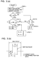
- pulse start data and that of pulse end data are carried out in accordance with the flow chart shown in Fig. 3(a).
- recording position data and density data are inputted into the pulse start and end data generating circuit 261 (step 1), it is judged whether or not value K of the recording position data is not less than 128(step 2).
- value K of the recording position data is not less than 128(step 2).
- 1/2 of value D of density data is not less than (255-K) (step 3).
- the waveform of a pulse shown in the drawing shows a case in which a writing operation is carried out by the laser writing device 430 at a high level.
- Figs. 4(a) - 4(h) are time charts in the case of generation of a writing pulse that is a modulation signal.
- Fig. 4(a) denotes an image clock
- Fig. 4(b) denotes density data
- Fig. 4(c) denotes recording position data
- Fig. 4(d) denotes pulse start data
- Fig. 4(e) denotes pulse end data
- Fig. 4(f) denotes trigger pulse t1 that will be described later
- Fig. 4(g) denotes trigger pulse t2 that will be described later
- Fig. 4(h) denotes a pulse of the aforementioned modulated writing signal.
- the pulse start data is inputted into the programmable delay generator A262, and trigger pulse t1 delayed by the amount of A with respect to the start point of the period is sent to the D type flip flop 264.
- the pulse end data is inputted into the programmable delay generator B263, and trigger pulse t2 delayed by the amount of B with respect to the start point of the period is inputted into the D type flip flop 264.
- the writing pulse shown in Fig. 4(h) is generated and sent to the laser writing device 430 from terminal Q of the D type flip flop 264.
- the recording position data is set at 128, and the recording position modulation is not carried out.
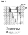
- recording position modulation is carried out in the following manner: the positions of small dots on n lines in the objective pixels are displaced in the direction of the line of the original characters and line images compared with the density data of the original adjacent pixels as shown in Fig. 6. As a result, characters and line images can be reproduced clearly.
- recording is carried out by the unit of 2 dots, so that half-tone images of high gradation can be reproduced.
- a half-tone dot having a screen angle can be provided.
- the screen angle of yellow components is set at 45°
- that of magenta components is set at 26.6°
- that of cyan components is set at -26.6°
- that of black components is set at 0°
- the uniformity of color reproduction can be improved and the occurrence of moire stripes can be prevented.
- the aforementioned modulation means can be used as it is.
- the raster scanning circuit 300 includes a ⁇ delay circuit 311, 2 ⁇ delay circuit 312, laser drivers 301A to 301C, index detection circuit (not shown), and polygonal mirror driver.
- the laser drivers 301A to 301C oscillate the semiconductor array 431 having a plurality of laser beam emitting portions 431A to 431C in accordance with the modulation signal sent from the modulation circuits 260A to 260C.
- a signal corresponding to the amount of beam sent from the semiconductor array 431 is fed back to the laser drivers, and the laser drivers 301A to 301C drive the semiconductor array 431 so that the amount of beam can be constant.
- the index detection circuit detects the position of the surface of the rotational polygonal mirror 434 rotating at a predetermined speed by the index signal sent from the index sensor 439 shown in Fig. 7, so that optical scanning is conducted by the raster scanning system in accordance with the modulated image density signal at the period of primary scanning.
- the scanning frequency is 2204.72 Hz
- the effective printing width is 297 mm
- the effective exposure width is 306 mm.
- the polygonal mirror driver includes a DC motor rotating at a predetermined speed so that the rotational polygonal mirror 434 is rotated at the speed of 16535.4 rpm.
- the semiconductor array 431 includes three light emitting portions 431A to 431C that are disposed at regular intervals forming an array.
- the light emitting portions are disposed as shown in Fig. 8 in the following manner: an axis passing through the centers of the light emitting portions 431A to 431C is set in parallel with the rotational shaft of the rotational polygonal mirror 434, and the axis is inclined by a predetermined angle with respect to the primary scanning direction.
- laser beam spots sa, sb and sc formed on the photoreceptor 401 by the semiconductor laser array 431 scan the photoreceptor surface in such a manner that the intervals between the spots are very close as illustrated in Fig. 9.
- the positions of laser beam spots sa, sb and sc are shifted with respect to the primary scanning direction.
- the ⁇ delay circuit 311 is provided between the modulation circuit 260B and the laser driver 301B
- the 2 ⁇ delay circuit 312 is provided between the modulation circuit 260C and the laser driver 301C, so that the signals are appropriately delayed. In this way the shifted position can be corrected.
- laser beam spots sa, sb and sc emitted from the semiconductor array 431 are changed into sa', sb' and sc' vertically aligned with respect to the primary scanning direction. Recording is carried out by these laser beam spots sa', sb' and sc'.
- image recording is carried out in the following manner: average density data and recording position data of each small scanning line obtained by the RE processing circuit 240 is inputted into the modulation circuits 260A to 160C; and the writing pulse obtained in the aforementioned process is inputted into the laser drivers 301A to 301C so as to record the image.
- image processing can be also provided.
- image processing can be carried out in the following manner: For example, an intermediate value 128 is inputted into the modulation circuits 260A to 260C as image data; only recording position modulation is conducted by the recording position data obtained in the RE processing circuit 240; the average density data in pixel m5 on each small scanning line outputted from terminals O4 to O6 of the RE processing circuit 240 is converted into an analog value; and the obtained analog value is inputted into each of the laser drivers 301A to 301C so that the drive current can be controlled so as to control the output of light emission of the semiconductor lasers 431A to 431C.
- Fig. 16 is a graph showing an example of the relation between the drive current of a semiconductor laser and the output of emission of laser beams.
- the photoreceptor drum 401 is uniformly charged with electricity by the scorotron charger 402.
- An electrostatic latent image corresponding to yellow is formed on the surface of the photoreceptor drum 401 in the following manner: a laser beam modulated by yellow data (8-bit digital density data) sent from the image density data storage circuit 210 is irradiated on the photoreceptor drum 401 through the cylindrical lens 433, rotational polygonal mirror 434, f ⁇ lens 435, cylindrical lens 436 and reflection mirror 437.
- the electrostatic latent image corresponding to yellow is developed by the first developing unit 441, so that a very sharp dot-shaped first toner image (yellow toner image) is formed on the photoreceptor drum 401. This first toner image is not transferred onto a recording paper but passes under the cleaning unit 470 that has been withdrawn. Then, the photoreceptor drum is electrically charged again by the scorotron charger 402.
- a laser beam modulated by magenta data (8-bit digital density data) is irradiated on the photoreceptor drum 401 so that an electrostatic latent image is formed.
- This electrostatic latent image is developed by the second developing unit 442 so that the second toner image (magenta toner image) is formed.
- the third toner image (cyan toner image) is formed by the third developing unit 443.
- These toner images are successively accumulated on the surface of the photoreceptor drum 401 so that a 3-color toner image can be formed.
- the fourth toner image black toner image
- a 4-color toner image is formed on the photoreceptor drum 401.
- An excellent photoreceptor having high ⁇ property is used for the photoreceptor drum 401 of the image forming apparatus of this example. Therefore, an electrostatic latent image can be stably formed even when charging, exposing and developing operations are repeatedly conducted on a toner image. That is, even when a laser beam modulated in accordance with a digital signal is irradiated on a toner image, a highly sharp dot-shaped electrostatic latent image without any fringes can be formed. As a result, a sharp toner image can be provided.
- These 4-color toner image is transferred by the action of the transfer unit 462 onto a recording paper supplied from a paper supply unit.
- the transferred recording paper is separated from the surface of the photoreceptor 401 by the separator 463, and conveyed by a guide and a conveyance belt to the fixing roller 464 so that the transferred toner image is thermally fixed. Then, the recording sheet is discharged onto a paper discharge tray.
- P can be used as a constant, it is preferable that P is changed in synchronization with the recording period, that is, corresponding to the image (in a character region or half-tone region).
- P1 in the case where the recording period is short, that is, the image is in the character region
- P2 in the case where the recording period is long, that is, the image is in the half-tone region
- P1 > P2 is preferable. That is, when the image exists in the character region, the value of P is large, preferably 0.9 to 0.4, and when the image exists in the half-tone region, the value of P is small, preferably 0.6 to 0.1.
- P 0 corresponds to the value in the case where recording position modulation is not conducted.
- the ratio of RE processing can be changed.
- Fig. 17 is a graph showing an example of the case where the relation between the recording position in the primary scanning direction and the gravity center is converted.
- Fig. 18 is a graph showing an example of the case where the average density in the auxiliary scanning direction is converted.
- the recording position can be changed according to a conversion equation which is set beforehand, for example, as shown in Fig. 17 using a ROM 245 in which the result obtained from the image density data by arithmetic processing is contained, or on which the above result is provided externally.
- the average density data of small scanning line can be also changed as shown in Fig. 18.
- the ratio of conversion shown in Fig. 17, and Fig. 18 is changed corresponding to the case where the image clock is changed.
- gradation is considered to be important, and the ratio of the recording position modulation is decreased, or ⁇ of gradation is decreased.
- the present invention is not limited to the specific embodiments, but when the image data processing circuit 100 is replaced by the image data processing circuit 150 composed of the color scanner 151, the A/D converter 152, the density converter 153, the masking UCR circuit 154 and the like, and the image density data is inputted into the processing circuit 150 from the scanner and the image is processed in the circuit, the present invention can be adopted to other image forming apparatus such as a copying apparatus and the like.
- the image clock is changed over for each pixel in accordance with the result of image discrimination.
- the external command such as characters and a photographic mode.
- the RE processing is carried out in the following manner: in accordance with the density data of the objective pixel, with respect to the objective pixel included in the specific density, the objective pixel is divided into small pixels, and the density of the objective pixel is distributed to each small pixel according to the density distribution of adjacent pixels including the objective pixel.
- the recording position data corresponding to the position of the gravity center of density of the image data that has been subjected to the RE processing, and the average density data of each small scanning line are found, and a modulation means is provided that generates a writing pulse not affecting the adjacent pixels that is recording-position-modulated and also pulse-width-modulated, and recording-position-modulation is not conducted with respect to the low and high density portions.
- the writing dot does not enter other pixels, so that they are not affected. Therefore, a recording image of high quality can be provided.
- image discrimination is conducted by the image discrimination circuit, and in the case of a character region, the writing operation is conducted by a short period of 1 dot, and in the case of a half-tone region, the writing operation is conducted by a long period of 2 dots so as to conduct color image recording. Consequently, the sharpness of a color image can be improved without fluctuation of color tone when the color image is formed in accordance with a scanner, CG or font data. Further, a high ⁇ type photoreceptor is applied to the apparatus of the present invention, so that the effects can be further improved.
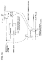
- Fig. 24 is a schematic illustration showing the structure of the essential portion of a digital copier (in which a laser beam is utilized) to which the present invention is applied.
- the scanner 1 obtains image information from an object to be copied.
- the obtained information is AD-converted and processed in the image processing section 2, and then the information is subjected to shading correction and others.
- the timing controller 4 sends the data to the printer 5 in synchronization with the image data transmission clock.
- the image formation signal generator 6 generates an image formation signal S (a signal for reproduction of gradation by a PWM pulse) in accordance with inputted image data D (8 bit data).
- the laser drive circuit 7 drives the semiconductor laser 8.
- a scanning operation is conducted on the laser beam by the polygonal mirror 11. Due to the scanning operation, an electrostatic latent image is formed on the photoreceptor drum.
- Numeral 9 is a timing circuit
- numeral 19 is a motor drive circuit
- numeral 12 is an index sensor
- numeral 13 is an I/V amplifier.
- the present invention is applied to the PWM pulse generation circuit for reproduction of gradation provided in the image formation signal generation circuit 6 shown in Fig. 19.
- Fig. 19 is a schematic illustration showing the structure of the second example of the present invention.
- This example includes a digital programmable delay generator 510 and a D-type flip flop 520, and a PWM pulse (PWM OUT) for reproduction of gradation having a pulse width corresponding to the input image data is generated in this example.
- the trigger input of the digital programmable delay generator 510 is the image data transmission clock, and the data input is the image data of 8 bits.
- the data input terminal of the D type flip flop 520 is always pulled up to a high level. Also, the image data transmission clock is inputted into the clock terminal of the flip flop 520, and the flip flop 520 is reset by a delay pulse that is the output of the digital programmable delay generator 510.
- the output of the D type flip flop 520 is raised up to a high level by the positive edge of the image transmission clock.
- the D type flip flop 520 is reset by the positive edge of the delay pulse of the digital programmable delay generator 510 so that the output of the D type flip flop 520 is returned to a low level.
- a pulse width signal PWM OUT is generated in accordance with the image data information.
- a reset pulse to determine the pulse width is generated by the digital programmable delay generator 510 that can change the delay amount in accordance with the input digital data. Therefore, an externally provided analog circuit, which is susceptible to the influence of peripheral circuits, can be eliminated. For that reason, highly accurate PWM pulses can be generated without being affected by noise. Further, only the image data and its transmission clock are used for the signal inputted into the circuit, and it is not necessary to use other control signals, so that the structure can be simplified. Consequently, the area on the system board occupied by the circuit can be reduced.
- Fig. 20 is a schematic illustration showing the structure of the third example of the present invention.
- the basic structure of this example is the same as that of the example explained before, the 2-frequency demultiplier 530, selector 540 and switching circuit 550 are added to this third example.
- image quality can be enhanced when the gradation reproduction accuracy is improved by generating one PWM pulse while pieces of information of a plurality of adjacent pixels are averaged even if the resolution is deteriorated, rather than processing is conducted for each pixel.
- the function of the aforementioned example can be applied even in the case where a plurality of pixels are processed in a lump.
- the circuit is structured so that processing can be carried out for each 2 pixels.
- the clock of one pixel period and the cycle dividing clock sent from the 2-frequency demultiplying circuit 530 can be selected by the selector 540.
- Concerning the image data the data for each pixel and the average of the data of 2 pixels can be selected and outputted by the selecting circuit 550.
- the maximum delay amount of the digital programmable delay generator 510 can be changed into the delay scale of 2 pixels by the full scale delay range setting unit 560.
- the aforementioned signal selection control is carried out in accordance with the selection control signal (the printing period control signal) that is changed over between one and two pixels.
- the example when a minimized circuit is added, the example can be applied to a case in which data processing is carried out over a plurality pixels. Therefore, the following effects can be provided: an accurate PWM pulse is generated without being affected by noise; and the gradation is reproduced corresponding to the object to be copied.
- Fig. 21 is a block diagram showing an example of the structure in which the example shown in Fig. 20 is further specified.
- numeral 20 is an inverter
- numerals 21 and 22 are input buffer
- numeral 23 is a 2-frequency demultiplier circuit
- numeral 24 is a multiplexer for changing over between a clock at one pixel and a clock at each two pixels.
- the latches 25, 26 and 27 having enabling terminals, and the data adder 28 compose a data changeover circuit (corresponding to the circuit 550 shown in Fig. 20).
- Numerals 29, 30 and 31 denote latches for adjusting the timing used for synchronizing the image data with the full scale delay range setting signal.
- the delay line 33 is provided for adjusting the input timing to the D-type flip flop 36 of the image transmission clock, giving consideration to the fixed delay amount of the programmable delay generator 34 and the fixed delay amount of the inverter 35.
- the digital programmable delay generator 34 is structured in the manner shown in Fig. 23.
- the digital programmable delay generator 34 includes the digital data latch 50 of 8 bits, D/A converter 51, trigger circuit 52, lamp circuit 53 and comparator 54, and these components are integrated into one chip (IC).
- the adjusting terminal of the lamp circuit 53 is connected with the full scale delay range setting device (including a transistor T r for selecting a time constant, parallel resistances, and condensers) 32.
- image data is carried out for each two pixels and also for each one pixel in the following manner: one of the latches 25 and 26 is selected; the output data of the selected latch is added to the output data of the latch 27 that is always used (adder 28); and the added output is made to be 1/2.
- adder 28 When the added data is made to be 1/2, a particular circuit is not used but conducted in the following manner: in the case where data is inputted into the trigger terminal of the digital programmable delay generator 34, the input bit is shifted by one bit.
- one of the data changeover circuits 25 and 26 is compensationally becomes active in accordance with the level of the printing period control signal (printing 2).
- the latch 27 is always operated.
- the operational clock of the latch 25 is an image transmission clock (1PIX) for each one pixel
- the operational clock of the latch 26 is an image transmission clock (2PIX) for each two pixels.
- Fig. 22 is a timing chart for explaining the operation of this example.
- the reference characters shown in Fig. 22 denote the following signals.
- Printing 1 printing period control signal
- Printing 2 printing period control signal that has passed through the buffer 22
- DATA 1 digital image data
- DATA 2 digital image data that has passed through the buffer 21
- CLK 1 image transmission clock
- CLK 2 image transmission clock provided when CLK 1 is inverted by the inverter 20
- CLK 3 image transmission clock provided when CLK 2 is inverted by the inverter 37
- CLK 4 image transmission clock provided when CLK 2 is divided with the D-type flip flop 30
- 1PIX clock for arithmetic processing for each one pixel 2PIX: clock for arithmetic processing for each two pixels
- S-OUT 1 image transmission clock selected by the multiplexer 24 in accordance with the printing period control signal (printing 2)
- S-OUT 2 digital addition image data provided when the image data added by the adder 28 is latched with the image transfer clock (CLK 3)
- S-OUT 3 printing period control signal latched by the image transmission clock (CLK 2) in the latch 31 IN1: digital image data of one
- the full scale delay range of the digital programmable delay generator 34 is changed over to a value suited to generate a PWM pulse for each 2 pixels.
- the full scale delay range of the digital programmable delay generator 34 becomes a value suited to generate a PWM pulse for each one pixel.
- the changeover operation between a series of processing for each two pixels and a series of processing for each one pixel is systematically conducted when the level of printing control signal (printing 2) is changed over.
- This example is composed of an essential digital circuit including a multiplexer, adder and a plurality of latches, so that the structure is simple and the circuit can be structured of ICs, which can be easily realized.
- Fig. 25 is a schematic illustration showing the structure of the fifth example of the present invention.
- This example shows a gradation reproduction apparatus operated in accordance with a PWM signal, wherein the gradation reproduction apparatus can be applied to a digital color copier by which a document image is read, and also can be applied to a printer connected with a computer to which the image data is supplied from a data source.
- Image data is supplied by the print-out command unit 601.
- a document image is read by the scanner 603.
- Image data is temporarily stored in the frame memory 602. Then, the stored data is read out by the readout circuit 604 in synchronization with a reference clock supplied from the reference clock generating circuit 605.
- the PWM signal generating unit 607 generates a pulse width signal to control the light emitting time of the laser diode 612.
- the PWM signal generating unit 607 includes the density change detecting circuit 608 to detect the density change of an image, a plurality of kinds of PWM signal making and processing units 609 (one-pixel processing unit 609a in central portion, modulation processing unit 609b for recording position at edge portion, and two-pixel processing unit 609c in central portion), and the selector 610 that selectively outputs a necessary PWM signal.
- the plurality of kinds of PWM signal making and processing units 609 essentially includes the D/A converter 620, triangular wave (reference wave) generating circuit 621, and analog comparator 622.
- Information to be selected by the selector 610 is given to the selector 610 by the density change detecting circuit 608 and the photograph/character mode selecting circuit 606.
- a PWM signal sent from the modulation processing unit 609b for recording position at edge portion is selected and outputted, so that recording position modulation is realized for emphasizing the edge portions.
- gradation reproduction of high resolution is carried out with respect to the image center by a PWM signal through one pixel processing (that is, the PWM signal sent from 609b is selected).
- reproduction of high gradation is carried out with respect to the image center by a PWM signal corresponding to two-pixel processing (that is, the PWM signal sent from 609c is selected).
- the laser diode 612 is driven and scanned by the raster scanning circuit 611, so that an electrostatic latent image is formed on the surface of the photoreceptor drum 613.
- Image formation is achieved when the following operations are repeated: a charging operation conducted by the charger 402, an image exposing operation conducted by the laser diode 612, and a developing operation conducted by one of the color developing units 441 to 444. In this way, 4 color toner images are superimposed, and then the superimposed images are transferred. After transfer, the residual toner on the photoreceptor is removed by the cleaning means 470.
- Fig. 26 is a schematic illustration for explaining the effects of this example, that is, Fig. 26 is a view showing a model of the circumstances in which an electrostatic latent image is formed on the surface of the photoreceptor drum 613.
- the upper half portion is a character recording region
- the lower half portion is a photographic image recording region.
- the character recording region recording of high resolution is conducted by one pixel PWM in the center (region A) of a character.
- region B the recording position is shifted laterally (that is, the recording position is shifted from the position shown by a broken line to the hatched region), so that the occurrence of white spots is prevented and the sharpness is improved.
- recording is conducted by a PWM signal over two pixels in the image center (that is, in the half-tone region C of the image), so that the image is provided with high gradation.
- the edge portion of the image that is, in a region D in which a step-like density change exists in some portions
- recording position modulation is conducted in the same manner as in the character recording region, so that the contrast of density is emphasized.
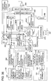
- Fig. 27 is a view showing the structure of the sixth example of the present invention.
- Numeral 100 corresponds to the print-out command unit 601 shown in Fig. 25, and numeral 150 corresponds to the scanner 603 in Fig. 25.
- Numeral 210 is a frame memory
- numeral 200 is a reading circuit
- numeral 280 is a reference clock generating circuit
- numeral 241 is an arithmetic circuit to detect the density change by taking the difference of pixel density.
- Numeral 283 is a 2-frequency demultiplier circuit of the reference clock
- numeral 230 is a delay circuit for adjusting the timing.
- Numerals 260A, 260B and 260C and the switching circuit 270 compose various PWM signal generating circuits corresponding to 609a to 609c in Fig. 25.
- Numerals 271 and 272 are delay circuits for adjusting the timing, and the selecting circuit 250 corresponds to the selector 610 shown in Fig. 25.
- Switching signals S0 and S1 are supplied to the selecting circuit 250 from the arithmetic circuit 241. Also, a mode switching signal for switching between the photographic mode and the character mode is supplied to the selecting circuit 250 from the outside of the circuit.
- the selecting circuit 250 selects and outputs one of the signals PWM1 (or PWM4), PWM2 and PWM3 in accordance with the switching signals S0 and S1 sent from the arithmetic circuit 241. One of PWM1 and PWM4 is selected and outputted in accordance with the character mode or the photographic mode switched by a mode switching signal.
- PWM1 is a pulse width signal for each pixel for use in the image center that is outputted from the PWM signal generating circuit 260A
- PWM2 and PWM3 are pulse width signals for recording position modulation at the edge portion that are outputted from the switching circuit 270.
- PWM4 is a pulse width signal over 2 pixels for a half-tone portion of a photographic image.
- PWM2 and PWM3 for recording position modulation are pulse width signals having a period corresponding to 2 pixel data, the phases of which are different from each other by 180°.
- One of PWM2 and PWM3 is appropriately selected by the switching circuit 250 in accordance with the recording position that is shifted to the right or the left.
- Numeral 300 is a raster scanning circuit.
- the MTF correcting circuit 274 is provided to the output section of the reading circuit 220. Also, in order to improve the gradation property, a ⁇ converting circuit is provided immediately before the D/A converting sections 262A to 262C (although the ⁇ converting circuit is not shown in the drawing). These circuits are changed over in accordance with the result of image density discrimination conducted by the arithmetic circuit 241 so that the gradation property of a recorded image can be guaranteed. In this way, the sharpness and the gradation property can be further improved.
- Fig. 28 is a timing chart showing an example of the operation of this example.
- the arithmetic circuit 241 takes the continuously inputted image density data of a unit of one scanning line in synchronization with the rising clock, and difference calculation is successively executed between the pixel data immediately before and after the image data to be recorded. This difference calculation is conducted in the following manner: the pixel data recorded immediately before is subtracted from the pixel data that immediately follows the image data to be recorded.
- the arithmetic circuit 241 is operated in the following manner: the difference value is compared with a specific value ⁇ ; in the case where the difference value is not less than ⁇ , the switching output S0 is made to be "1"; in the case where the difference value is smaller than - ⁇ , the switching output S1 is made to be "1"; and in the case of - ⁇ ⁇ difference value ⁇ ⁇ , both S0 and S1 are made to be "0". That is, in the case where S0 is "1", the density of the pixel recorded immediately after is higher than that of the pixel recorded immediately before. In the case where S1 is "1", the density of the pixel recorded immediately before is higher. Both S0 and S1 are "0", the density change is small.
- These switching signals S0 and S1 are supplied to the selecting circuit 250, and a PWM signal is selected in accordance with the information of the signal as described above.
- ⁇ T1, ⁇ T2 and ⁇ T3 are respectively the outputs of the triangular wave generators 262A, 263B and 263C in the PWM signal generators 260A, 260B and 260C shown in Fig. 27.
- Fig. 29 is a schematic illustration showing the circumstances of the generation of PWM signals in this example.
- OUT1, OUT2 and OUT3 shown in the lower portion of the drawing are respectively the outputs of 260A, 260B and 260C, which are PWM signals that have not been delayed.
- OUT4 is a PWM signal delayed by the delay circuit 272, wherein OUT4 is the aforementioned PWM4.
- Fig. 30 is a schematic illustration showing an example of the latent image forming position on the photoreceptor in the case where recording position modulation is carried out using the PWM signals (OUT1, OUT2 and OUT3, that is, PWM1, PWM2 and PWM3) shown in Fig. 29.
- the recording position is corrected in accordance with switching signals S0 and S1
- the formation positions of the pixels 2 and 4 are shifted to the side of the pixel 3, so that a sharp image in which white spots are reduced can be formed.
- (2) shows this example
- (1) shows a comparative example in which an ordinary pulse width modulation is carried out.
- Fig. 31 is a timing chart in the case where a difference calculation method is adopted for the density change detection in the calculation circuit 241 shown in Fig. 27, wherein the difference between the objective pixel and the pixel immediately before the objective pixel is taken in the difference calculation method.
- Fig. 32 is a view showing the effects of recording position modulation in that case. It can be understood that a sharp image formation can be carried out in the same manner as the cases shown in Figs. 28 and 30.
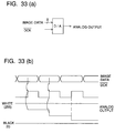
- Figs. 33(a) and 33(b) are schematic illustrations respectively showing the structure and operation of the D/A converters 262A, 262B and 262C shown in Fig. 27.
- Figs. 34(a) and 34(b) are schematic illustrations respectively showing the structure and operation of the triangular wave generation circuits 263A, 263B and 263C shown in Fig. 27.
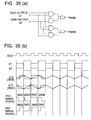
- Figs. 35(a) and 35(b) are schematic illustrations respectively showing the structure and operation of the switching circuit 270 shown in Fig. 27.
- Fig. 36 is a schematic illustration showing the structure of the seventh example of the present invention.
- a triangular wave is selected by the selecting circuit 250; and a PWM signal is finally generated by the analog comparator 268 (in the case shown in Fig. 27, a plurality of kinds of PWM signals are generated, and one of them is selected by the selecting circuit).
- a selector signal to select a reference wave in accordance with the result of image discrimination is inputted into the ⁇ converting circuit 273, and the gradation property is corrected using a corresponding ⁇ correcting table.
- the number of comparators to generate PWM signals is only one, so that the circuit can be simplified.
- the selecting circuit 606 is used for the selection of the photographic and character modes.
- the following structure may be employed: the density distribution pattern information taking function is added to the density change detection circuit 608; according to the result of the comparison between the pattern information and the table, the character and photographic regions are separated in accordance with the change of the density distribution in real time in the process of recording; and a switching operation is conducted between one and two pixel PWM signals.
- recording position modulation may be conducted in accordance with two dimensional density distribution information of the adjacent pixels in which the auxiliary scanning direction is considered.
- tables may be prepared respectively corresponding to photographic and character images, and in accordance with the result of discrimination between photographic and character images, an amount of shift of recording position may be changed over so that the amount is small in the photographic region and the amount is large in the character region.
- the reason why the aforementioned operation is conducted is as follows: the image quality is deteriorated when the contrast is too high in the case of a photographic image.
- the changeover operation is carried out in the aforementioned manner, characters of a sharp contour can be reproduced, and appropriate contrast of a photographic image can be realized.
Landscapes
- Engineering & Computer Science (AREA)
- Multimedia (AREA)
- Signal Processing (AREA)
- Facsimile Image Signal Circuits (AREA)
- Fax Reproducing Arrangements (AREA)
Applications Claiming Priority (6)
| Application Number | Priority Date | Filing Date | Title |
|---|---|---|---|
| JP84129/92 | 1992-04-06 | ||
| JP4084129A JPH05292297A (ja) | 1992-04-06 | 1992-04-06 | 画像形成装置 |
| JP4085476A JPH05292273A (ja) | 1992-04-07 | 1992-04-07 | 画像形成装置 |
| JP85476/92 | 1992-04-07 | ||
| JP09068092A JP3224264B2 (ja) | 1992-04-10 | 1992-04-10 | 画像形成装置 |
| JP90680/92 | 1992-04-10 |
Publications (2)
| Publication Number | Publication Date |
|---|---|
| EP0564868A2 true EP0564868A2 (fr) | 1993-10-13 |
| EP0564868A3 EP0564868A3 (en) | 1993-11-10 |
Family
ID=27304455
Family Applications (1)
| Application Number | Title | Priority Date | Filing Date |
|---|---|---|---|
| EP19930104445 Withdrawn EP0564868A3 (en) | 1992-04-06 | 1993-03-18 | Image forming apparatus |
Country Status (1)
| Country | Link |
|---|---|
| EP (1) | EP0564868A3 (fr) |
Cited By (6)
| Publication number | Priority date | Publication date | Assignee | Title |
|---|---|---|---|---|
| EP0723362A1 (fr) * | 1995-01-18 | 1996-07-24 | Canon Kabushiki Kaisha | Dispositif de formation d'image en couleur |
| EP0892551A2 (fr) * | 1997-07-15 | 1999-01-20 | Kabushiki Kaisha Toshiba | Dispositif de traitement d'image, appareil d'enregistrement d'image, dispositif de lecture d'image et appareil de formation d'image |
| US6166821A (en) * | 1998-10-02 | 2000-12-26 | Electronics For Imaging, Inc. | Self calibrating pulse width modulator for use in electrostatic printing applications |
| US6190058B1 (en) * | 1994-12-20 | 2001-02-20 | Canon Kabushiki Kaisha | Image processing method and apparatus and image forming method and apparatus using the same |
| WO2003036937A1 (fr) * | 2001-10-24 | 2003-05-01 | OCé PRINTING SYSTEMS GMBH | Procede pour la generation d'images de chargement d'images a imprimer sur un support intermediaire photoconducteur en mouvement d'une imprimante ou d'une photocopieuse electrophotographique |
| US7929183B2 (en) | 2003-03-27 | 2011-04-19 | Seiko Epson Corporation | Image output control system, image processing device, and image processing method |
Citations (6)
| Publication number | Priority date | Publication date | Assignee | Title |
|---|---|---|---|---|
| EP0204094A2 (fr) * | 1985-03-30 | 1986-12-10 | Hitachi, Ltd. | Procédé d'impression du type d'enregistrement par balayage et appareil pour le mettre en oeuvre |
| EP0212990A2 (fr) * | 1985-08-29 | 1987-03-04 | Canon Kabushiki Kaisha | Appareil de traitement d'images |
| US4868684A (en) * | 1986-04-03 | 1989-09-19 | Canon Kabushiki Kaisha | Image processing apparatus |
| WO1991016784A2 (fr) * | 1990-04-26 | 1991-10-31 | Zed Instruments Limited | Gravure d'un cylindre d'impression |
| US5081631A (en) * | 1991-04-03 | 1992-01-14 | Eastman Kodak Company | Direct modulation of laser diodes for radiographic printers |
| EP0528618A2 (fr) * | 1991-08-21 | 1993-02-24 | Konica Corporation | Appareil de formation d'images |
-
1993
- 1993-03-18 EP EP19930104445 patent/EP0564868A3/en not_active Withdrawn
Patent Citations (6)
| Publication number | Priority date | Publication date | Assignee | Title |
|---|---|---|---|---|
| EP0204094A2 (fr) * | 1985-03-30 | 1986-12-10 | Hitachi, Ltd. | Procédé d'impression du type d'enregistrement par balayage et appareil pour le mettre en oeuvre |
| EP0212990A2 (fr) * | 1985-08-29 | 1987-03-04 | Canon Kabushiki Kaisha | Appareil de traitement d'images |
| US4868684A (en) * | 1986-04-03 | 1989-09-19 | Canon Kabushiki Kaisha | Image processing apparatus |
| WO1991016784A2 (fr) * | 1990-04-26 | 1991-10-31 | Zed Instruments Limited | Gravure d'un cylindre d'impression |
| US5081631A (en) * | 1991-04-03 | 1992-01-14 | Eastman Kodak Company | Direct modulation of laser diodes for radiographic printers |
| EP0528618A2 (fr) * | 1991-08-21 | 1993-02-24 | Konica Corporation | Appareil de formation d'images |
Cited By (8)
| Publication number | Priority date | Publication date | Assignee | Title |
|---|---|---|---|---|
| US6190058B1 (en) * | 1994-12-20 | 2001-02-20 | Canon Kabushiki Kaisha | Image processing method and apparatus and image forming method and apparatus using the same |
| EP0723362A1 (fr) * | 1995-01-18 | 1996-07-24 | Canon Kabushiki Kaisha | Dispositif de formation d'image en couleur |
| US6674547B1 (en) | 1995-01-18 | 2004-01-06 | Canon Kabushiki Kaisha | Image processing apparatus for performing image formation using signals obtained by pulse-width modulating an image signal by a plurality of modulating methods |
| EP0892551A2 (fr) * | 1997-07-15 | 1999-01-20 | Kabushiki Kaisha Toshiba | Dispositif de traitement d'image, appareil d'enregistrement d'image, dispositif de lecture d'image et appareil de formation d'image |
| EP0892551A3 (fr) * | 1997-07-15 | 1999-12-29 | Kabushiki Kaisha Toshiba | Dispositif de traitement d'image, appareil d'enregistrement d'image, dispositif de lecture d'image et appareil de formation d'image |
| US6166821A (en) * | 1998-10-02 | 2000-12-26 | Electronics For Imaging, Inc. | Self calibrating pulse width modulator for use in electrostatic printing applications |
| WO2003036937A1 (fr) * | 2001-10-24 | 2003-05-01 | OCé PRINTING SYSTEMS GMBH | Procede pour la generation d'images de chargement d'images a imprimer sur un support intermediaire photoconducteur en mouvement d'une imprimante ou d'une photocopieuse electrophotographique |
| US7929183B2 (en) | 2003-03-27 | 2011-04-19 | Seiko Epson Corporation | Image output control system, image processing device, and image processing method |
Also Published As
| Publication number | Publication date |
|---|---|
| EP0564868A3 (en) | 1993-11-10 |
Similar Documents
| Publication | Publication Date | Title |
|---|---|---|
| US5432611A (en) | Image forming apparatus with sub-pixel position control | |
| EP0528365B1 (fr) | Appareil de formation d'images | |
| EP0527574B1 (fr) | Appareil de formation d'images | |
| EP0533377B1 (fr) | Procédé de formation d'images | |
| EP0540221B1 (fr) | Appareil de formation d'images | |
| US5619242A (en) | Image forming apparatus with edge point detector based on image density charge | |
| EP0564868A2 (fr) | Appareil de formation d'images | |
| US5265196A (en) | Image forming apparatus | |
| JPH05292297A (ja) | 画像形成装置 | |
| JP3177782B2 (ja) | カラー画像形成装置 | |
| JP3551403B2 (ja) | 画像形成装置 | |
| JP3066775B2 (ja) | カラー画像形成装置 | |
| JP3131653B2 (ja) | 画像形成装置 | |
| JP3103987B2 (ja) | カラー画像形成装置 | |
| JP3116174B2 (ja) | 画像形成装置 | |
| JP3306520B2 (ja) | 画像形成装置 | |
| JP3306519B2 (ja) | 画像形成装置 | |
| JPH05167811A (ja) | 画像形成装置 | |
| JPH05183711A (ja) | 画像形成方法 | |
| JPH05183713A (ja) | 画像形成方法 | |
| JPH0561450A (ja) | 画像形成装置 | |
| JPH05260288A (ja) | 画像形成装置 | |
| JPH05130347A (ja) | 画像形成装置 | |
| JPH05130388A (ja) | 画像形成装置 | |
| JPH05177882A (ja) | 画像形成方法 |
Legal Events
| Date | Code | Title | Description |
|---|---|---|---|
| PUAI | Public reference made under article 153(3) epc to a published international application that has entered the european phase |
Free format text: ORIGINAL CODE: 0009012 |
|
| PUAL | Search report despatched |
Free format text: ORIGINAL CODE: 0009013 |
|
| AK | Designated contracting states |
Kind code of ref document: A2 Designated state(s): DE FR GB IT NL |
|
| AK | Designated contracting states |
Kind code of ref document: A3 Designated state(s): DE FR GB IT NL |
|
| 17P | Request for examination filed |
Effective date: 19940409 |
|
| 17Q | First examination report despatched |
Effective date: 19960424 |
|
| STAA | Information on the status of an ep patent application or granted ep patent |
Free format text: STATUS: THE APPLICATION HAS BEEN WITHDRAWN |
|
| 18W | Application withdrawn |
Withdrawal date: 19961107 |