EP0562571B1 - Module de circuit imprimé - Google Patents
Module de circuit imprimé Download PDFInfo
- Publication number
- EP0562571B1 EP0562571B1 EP93104823A EP93104823A EP0562571B1 EP 0562571 B1 EP0562571 B1 EP 0562571B1 EP 93104823 A EP93104823 A EP 93104823A EP 93104823 A EP93104823 A EP 93104823A EP 0562571 B1 EP0562571 B1 EP 0562571B1
- Authority
- EP
- European Patent Office
- Prior art keywords
- crystallites
- conductive
- layer
- circuit module
- adhesive
- Prior art date
- Legal status (The legal status is an assumption and is not a legal conclusion. Google has not performed a legal analysis and makes no representation as to the accuracy of the status listed.)
- Expired - Lifetime
Links
Images
Classifications
-
- H—ELECTRICITY
- H05—ELECTRIC TECHNIQUES NOT OTHERWISE PROVIDED FOR
- H05K—PRINTED CIRCUITS; CASINGS OR CONSTRUCTIONAL DETAILS OF ELECTRIC APPARATUS; MANUFACTURE OF ASSEMBLAGES OF ELECTRICAL COMPONENTS
- H05K1/00—Printed circuits
- H05K1/02—Details
- H05K1/09—Use of materials for the conductive, e.g. metallic pattern
- H05K1/092—Dispersed materials, e.g. conductive pastes or inks
- H05K1/095—Dispersed materials, e.g. conductive pastes or inks for polymer thick films, i.e. having a permanent organic polymeric binder
-
- H—ELECTRICITY
- H05—ELECTRIC TECHNIQUES NOT OTHERWISE PROVIDED FOR
- H05K—PRINTED CIRCUITS; CASINGS OR CONSTRUCTIONAL DETAILS OF ELECTRIC APPARATUS; MANUFACTURE OF ASSEMBLAGES OF ELECTRICAL COMPONENTS
- H05K3/00—Apparatus or processes for manufacturing printed circuits
- H05K3/30—Assembling printed circuits with electric components, e.g. with resistor
- H05K3/32—Assembling printed circuits with electric components, e.g. with resistor electrically connecting electric components or wires to printed circuits
- H05K3/321—Assembling printed circuits with electric components, e.g. with resistor electrically connecting electric components or wires to printed circuits by conductive adhesives
- H05K3/323—Assembling printed circuits with electric components, e.g. with resistor electrically connecting electric components or wires to printed circuits by conductive adhesives by applying an anisotropic conductive adhesive layer over an array of pads
-
- H—ELECTRICITY
- H01—ELECTRIC ELEMENTS
- H01L—SEMICONDUCTOR DEVICES NOT COVERED BY CLASS H10
- H01L2224/00—Indexing scheme for arrangements for connecting or disconnecting semiconductor or solid-state bodies and methods related thereto as covered by H01L24/00
- H01L2224/01—Means for bonding being attached to, or being formed on, the surface to be connected, e.g. chip-to-package, die-attach, "first-level" interconnects; Manufacturing methods related thereto
- H01L2224/26—Layer connectors, e.g. plate connectors, solder or adhesive layers; Manufacturing methods related thereto
- H01L2224/28—Structure, shape, material or disposition of the layer connectors prior to the connecting process
- H01L2224/29—Structure, shape, material or disposition of the layer connectors prior to the connecting process of an individual layer connector
- H01L2224/29001—Core members of the layer connector
- H01L2224/29099—Material
- H01L2224/29198—Material with a principal constituent of the material being a combination of two or more materials in the form of a matrix with a filler, i.e. being a hybrid material, e.g. segmented structures, foams
- H01L2224/29298—Fillers
- H01L2224/29499—Shape or distribution of the fillers
-
- H—ELECTRICITY
- H05—ELECTRIC TECHNIQUES NOT OTHERWISE PROVIDED FOR
- H05K—PRINTED CIRCUITS; CASINGS OR CONSTRUCTIONAL DETAILS OF ELECTRIC APPARATUS; MANUFACTURE OF ASSEMBLAGES OF ELECTRICAL COMPONENTS
- H05K1/00—Printed circuits
- H05K1/18—Printed circuits structurally associated with non-printed electric components
- H05K1/181—Printed circuits structurally associated with non-printed electric components associated with surface mounted components
-
- H—ELECTRICITY
- H05—ELECTRIC TECHNIQUES NOT OTHERWISE PROVIDED FOR
- H05K—PRINTED CIRCUITS; CASINGS OR CONSTRUCTIONAL DETAILS OF ELECTRIC APPARATUS; MANUFACTURE OF ASSEMBLAGES OF ELECTRICAL COMPONENTS
- H05K2201/00—Indexing scheme relating to printed circuits covered by H05K1/00
- H05K2201/02—Fillers; Particles; Fibers; Reinforcement materials
- H05K2201/0203—Fillers and particles
- H05K2201/0206—Materials
- H05K2201/023—Hard particles, i.e. particles in conductive adhesive at least partly penetrating an electrode
-
- H—ELECTRICITY
- H05—ELECTRIC TECHNIQUES NOT OTHERWISE PROVIDED FOR
- H05K—PRINTED CIRCUITS; CASINGS OR CONSTRUCTIONAL DETAILS OF ELECTRIC APPARATUS; MANUFACTURE OF ASSEMBLAGES OF ELECTRICAL COMPONENTS
- H05K2201/00—Indexing scheme relating to printed circuits covered by H05K1/00
- H05K2201/03—Conductive materials
- H05K2201/032—Materials
- H05K2201/0326—Inorganic, non-metallic conductor, e.g. indium-tin oxide [ITO]
-
- H—ELECTRICITY
- H05—ELECTRIC TECHNIQUES NOT OTHERWISE PROVIDED FOR
- H05K—PRINTED CIRCUITS; CASINGS OR CONSTRUCTIONAL DETAILS OF ELECTRIC APPARATUS; MANUFACTURE OF ASSEMBLAGES OF ELECTRICAL COMPONENTS
- H05K2201/00—Indexing scheme relating to printed circuits covered by H05K1/00
- H05K2201/10—Details of components or other objects attached to or integrated in a printed circuit board
- H05K2201/10613—Details of electrical connections of non-printed components, e.g. special leads
- H05K2201/10621—Components characterised by their electrical contacts
- H05K2201/10636—Leadless chip, e.g. chip capacitor or resistor
-
- Y—GENERAL TAGGING OF NEW TECHNOLOGICAL DEVELOPMENTS; GENERAL TAGGING OF CROSS-SECTIONAL TECHNOLOGIES SPANNING OVER SEVERAL SECTIONS OF THE IPC; TECHNICAL SUBJECTS COVERED BY FORMER USPC CROSS-REFERENCE ART COLLECTIONS [XRACs] AND DIGESTS
- Y02—TECHNOLOGIES OR APPLICATIONS FOR MITIGATION OR ADAPTATION AGAINST CLIMATE CHANGE
- Y02P—CLIMATE CHANGE MITIGATION TECHNOLOGIES IN THE PRODUCTION OR PROCESSING OF GOODS
- Y02P70/00—Climate change mitigation technologies in the production process for final industrial or consumer products
- Y02P70/50—Manufacturing or production processes characterised by the final manufactured product
-
- Y—GENERAL TAGGING OF NEW TECHNOLOGICAL DEVELOPMENTS; GENERAL TAGGING OF CROSS-SECTIONAL TECHNOLOGIES SPANNING OVER SEVERAL SECTIONS OF THE IPC; TECHNICAL SUBJECTS COVERED BY FORMER USPC CROSS-REFERENCE ART COLLECTIONS [XRACs] AND DIGESTS
- Y10—TECHNICAL SUBJECTS COVERED BY FORMER USPC
- Y10S—TECHNICAL SUBJECTS COVERED BY FORMER USPC CROSS-REFERENCE ART COLLECTIONS [XRACs] AND DIGESTS
- Y10S428/00—Stock material or miscellaneous articles
- Y10S428/901—Printed circuit
-
- Y—GENERAL TAGGING OF NEW TECHNOLOGICAL DEVELOPMENTS; GENERAL TAGGING OF CROSS-SECTIONAL TECHNOLOGIES SPANNING OVER SEVERAL SECTIONS OF THE IPC; TECHNICAL SUBJECTS COVERED BY FORMER USPC CROSS-REFERENCE ART COLLECTIONS [XRACs] AND DIGESTS
- Y10—TECHNICAL SUBJECTS COVERED BY FORMER USPC
- Y10T—TECHNICAL SUBJECTS COVERED BY FORMER US CLASSIFICATION
- Y10T428/00—Stock material or miscellaneous articles
- Y10T428/24—Structurally defined web or sheet [e.g., overall dimension, etc.]
- Y10T428/24802—Discontinuous or differential coating, impregnation or bond [e.g., artwork, printing, retouched photograph, etc.]
- Y10T428/24893—Discontinuous or differential coating, impregnation or bond [e.g., artwork, printing, retouched photograph, etc.] including particulate material
-
- Y—GENERAL TAGGING OF NEW TECHNOLOGICAL DEVELOPMENTS; GENERAL TAGGING OF CROSS-SECTIONAL TECHNOLOGIES SPANNING OVER SEVERAL SECTIONS OF THE IPC; TECHNICAL SUBJECTS COVERED BY FORMER USPC CROSS-REFERENCE ART COLLECTIONS [XRACs] AND DIGESTS
- Y10—TECHNICAL SUBJECTS COVERED BY FORMER USPC
- Y10T—TECHNICAL SUBJECTS COVERED BY FORMER US CLASSIFICATION
- Y10T428/00—Stock material or miscellaneous articles
- Y10T428/24—Structurally defined web or sheet [e.g., overall dimension, etc.]
- Y10T428/24802—Discontinuous or differential coating, impregnation or bond [e.g., artwork, printing, retouched photograph, etc.]
- Y10T428/24917—Discontinuous or differential coating, impregnation or bond [e.g., artwork, printing, retouched photograph, etc.] including metal layer
-
- Y—GENERAL TAGGING OF NEW TECHNOLOGICAL DEVELOPMENTS; GENERAL TAGGING OF CROSS-SECTIONAL TECHNOLOGIES SPANNING OVER SEVERAL SECTIONS OF THE IPC; TECHNICAL SUBJECTS COVERED BY FORMER USPC CROSS-REFERENCE ART COLLECTIONS [XRACs] AND DIGESTS
- Y10—TECHNICAL SUBJECTS COVERED BY FORMER USPC
- Y10T—TECHNICAL SUBJECTS COVERED BY FORMER US CLASSIFICATION
- Y10T428/00—Stock material or miscellaneous articles
- Y10T428/24—Structurally defined web or sheet [e.g., overall dimension, etc.]
- Y10T428/24802—Discontinuous or differential coating, impregnation or bond [e.g., artwork, printing, retouched photograph, etc.]
- Y10T428/24926—Discontinuous or differential coating, impregnation or bond [e.g., artwork, printing, retouched photograph, etc.] including ceramic, glass, porcelain or quartz layer
-
- Y—GENERAL TAGGING OF NEW TECHNOLOGICAL DEVELOPMENTS; GENERAL TAGGING OF CROSS-SECTIONAL TECHNOLOGIES SPANNING OVER SEVERAL SECTIONS OF THE IPC; TECHNICAL SUBJECTS COVERED BY FORMER USPC CROSS-REFERENCE ART COLLECTIONS [XRACs] AND DIGESTS
- Y10—TECHNICAL SUBJECTS COVERED BY FORMER USPC
- Y10T—TECHNICAL SUBJECTS COVERED BY FORMER US CLASSIFICATION
- Y10T428/00—Stock material or miscellaneous articles
- Y10T428/25—Web or sheet containing structurally defined element or component and including a second component containing structurally defined particles
Claims (5)
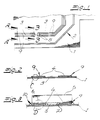
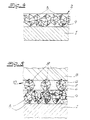
- Module de circuit imprimé pour des applications électroniques, incluant :un substrat de circuit (1) sur lequel est imprimée une couche d'encre (2), la couche d'encre comportant des rubans conducteurs de l'électricité (9) avec des zones de contact (4) conçues pour réaliser une connexion électrique avec des surfaces de contact (6) correspondantes d'un composant électronique (5) ;des cristallites conductrices (8) noyées à l'intérieur, formées à partir d'un composé cristallin inoxydable et d'un élément du sous-groupe IV de la Table Périodique, et de l'un des éléments du groupe constitué de l'azote et du carbone ; etune couche de colle (10) ;lesdites cristallites (8) étant également réparties dans ladite couche de colle (10) de façon à ne présenter aucun contact physique entre elles, et, par conséquent de façon telle que la colle soit non conductrice dans la direction parallèle à son plan de couche.
- Module de circuit imprimé pour des applications électroniques, incluant :un substrat de circuit (1) sur lequel est imprimée une couche d'encre (2), la couche d'encre comportant des rubans conducteurs de l'électricité (9) conçus pour réaliser une connexion électrique avec un composant électronique (5) ;des cristallites conductrices (8) noyées dans toute la couche d'encre imprimée (2), formées à partir d'un composé cristallin inoxydable et d'un élément du sous-groupe IV de la Table Périodique, et de l'un des éléments du groupe constitué de l'azote et du carbone ; etune couche de colle (10) ;lesdites cristallites (8) étant également réparties dans ladite couche de colle (10) de façon à ne présenter aucun contact physique entre elles, et, par conséquent de façon telle que la colle soit non conductrice dans la direction parallèle à son plan de couche.
- Module de circuit selon la revendication 1, dans lequel les cristallites sont constituées de nitrure de titane.
- Module de circuit selon la revendication 1, dans lequel les cristallites sont constituées de carbure de titane.
- Module de circuit selon la revendication 1, dans lequel la teneur en cristallites (8) de la couche de colle (10) est d'environ 10 %, en poids.
Applications Claiming Priority (2)
| Application Number | Priority Date | Filing Date | Title |
|---|---|---|---|
| DE4209597 | 1992-03-25 | ||
| DE4209597 | 1992-03-25 |
Publications (3)
| Publication Number | Publication Date |
|---|---|
| EP0562571A2 EP0562571A2 (fr) | 1993-09-29 |
| EP0562571A3 EP0562571A3 (fr) | 1994-02-09 |
| EP0562571B1 true EP0562571B1 (fr) | 1996-07-17 |
Family
ID=6454924
Family Applications (1)
| Application Number | Title | Priority Date | Filing Date |
|---|---|---|---|
| EP93104823A Expired - Lifetime EP0562571B1 (fr) | 1992-03-25 | 1993-03-24 | Module de circuit imprimé |
Country Status (3)
| Country | Link |
|---|---|
| US (1) | US5340640A (fr) |
| EP (1) | EP0562571B1 (fr) |
| DE (1) | DE69303645T2 (fr) |
Families Citing this family (13)
| Publication number | Priority date | Publication date | Assignee | Title |
|---|---|---|---|---|
| US6271482B1 (en) | 1994-08-23 | 2001-08-07 | Thomas & Betts International, Inc. | Conductive elastomer interconnect |
| US5949029A (en) * | 1994-08-23 | 1999-09-07 | Thomas & Betts International, Inc. | Conductive elastomers and methods for fabricating the same |
| US6580369B1 (en) * | 1995-10-11 | 2003-06-17 | Motorola, Inc. | Electronic tag assembly and method therefor |
| CN1420538A (zh) * | 1996-07-12 | 2003-05-28 | 富士通株式会社 | 半导体装置的制造方法和半导体装置及其装配方法 |
| US6881611B1 (en) * | 1996-07-12 | 2005-04-19 | Fujitsu Limited | Method and mold for manufacturing semiconductor device, semiconductor device and method for mounting the device |
| AU7683498A (en) * | 1998-06-02 | 1999-12-20 | Gintic Institute Of Manufacturing Technology | A method of mounting a semiconductor die on a printed circuit board |
| US6824857B2 (en) | 2001-04-02 | 2004-11-30 | Nashua Corporation | Circuit elements having an embedded conductive trace and methods of manufacture |
| EP1383364A3 (fr) * | 2002-05-23 | 2006-01-04 | Nashua Corporation | Eléments de circuit ayant un revêtement récepteur d'encre et une trace conductrice et leur procédé de fabrication |
| US6709944B1 (en) * | 2002-09-30 | 2004-03-23 | General Electric Company | Techniques for fabricating a resistor on a flexible base material |
| US20070246158A1 (en) * | 2006-04-21 | 2007-10-25 | 3M Innovative Properties Company | Wiring board, production process thereof and connection method using same |
| US8510935B2 (en) * | 2007-07-10 | 2013-08-20 | Joseph C Fjelstad | Electronic assemblies without solder and methods for their manufacture |
| GB2539684B (en) * | 2015-06-24 | 2018-04-04 | Dst Innovations Ltd | Method of surface-mounting components |
| MX2021003087A (es) * | 2018-09-17 | 2021-05-12 | Westrock Mwv Llc | Conjunto de circuitos y componentes de los mismos para embalaje. |
Family Cites Families (9)
| Publication number | Priority date | Publication date | Assignee | Title |
|---|---|---|---|---|
| US3875434A (en) * | 1973-10-31 | 1975-04-01 | Du Pont | Pressure-sensitive sensor/logic assembly |
| JPS605077B2 (ja) * | 1980-12-19 | 1985-02-08 | 松下電器産業株式会社 | メタライズ用組成物 |
| JPH0240710B2 (ja) * | 1982-03-26 | 1990-09-12 | Inoue Japax Res | Dodenseisetsuchakuzai |
| DE3443789A1 (de) * | 1983-12-02 | 1985-06-27 | Osaka Soda Co. Ltd., Osaka | Elektrische leitende klebstoffmasse |
| JPS61147593A (ja) * | 1984-12-20 | 1986-07-05 | 神東塗料株式会社 | 導電性接着剤層を付与したフレキシブル回路基材およびその製造方法 |
| JPS6241277A (ja) * | 1985-08-16 | 1987-02-23 | Shin Etsu Polymer Co Ltd | 異方導電性接着剤 |
| JPS62217694A (ja) * | 1986-03-18 | 1987-09-25 | ダイソー株式会社 | 回路の接続方法 |
| JPS62226688A (ja) * | 1986-03-27 | 1987-10-05 | 神東塗料株式会社 | ブリツジ用導電性ペ−スト組成物 |
| US4694572A (en) * | 1986-06-13 | 1987-09-22 | Tektronix, Inc. | Printed polymer circuit board method |
-
1993
- 1993-03-24 DE DE69303645T patent/DE69303645T2/de not_active Expired - Fee Related
- 1993-03-24 EP EP93104823A patent/EP0562571B1/fr not_active Expired - Lifetime
- 1993-03-24 US US08/036,309 patent/US5340640A/en not_active Expired - Fee Related
Also Published As
| Publication number | Publication date |
|---|---|
| US5340640A (en) | 1994-08-23 |
| EP0562571A3 (fr) | 1994-02-09 |
| DE69303645D1 (de) | 1996-08-22 |
| EP0562571A2 (fr) | 1993-09-29 |
| DE69303645T2 (de) | 1997-02-13 |
Similar Documents
| Publication | Publication Date | Title |
|---|---|---|
| EP0562571B1 (fr) | Module de circuit imprimé | |
| US5340641A (en) | Electrical overstress pulse protection | |
| EP0329782B1 (fr) | Numeriseur | |
| EP0400953A2 (fr) | Dispositif d'entrée | |
| DE3347848C2 (fr) | ||
| AU4825090A (en) | Improved method for making printed circuits | |
| GB2170365A (en) | Heat sensitive type adhesive connector | |
| EP0221924A1 (fr) | Cable electrique cavalier flexible et assemblage | |
| EP0110382A2 (fr) | Dispositif d'affichage et procédé pour sa réalisation et décalcomanie pour former un terminal de tableau d'affichage | |
| EP1189271A3 (fr) | Plaquettes de circuit et montage des dispositifs semiconducteurs au dessus de ces plaquettes | |
| GB2172441A (en) | Printed wiring board with key contacts | |
| EP1298967B1 (fr) | Carte électronique | |
| EP1082882A1 (fr) | Procede de fabrication de resistances | |
| EP0562569A2 (fr) | Colle anisotropique pour lier un composant électronique à un module de circuit imprimé | |
| KR920005071B1 (ko) | 배선기판 | |
| US4934470A (en) | Data input board | |
| EP0307007A3 (en) | Making electrical contact between metals and resistive emaking electrical contact between metals and resistive elements lements | |
| EP0605689B1 (fr) | Connexion electrique anisotrope | |
| JPS5951110B2 (ja) | 受光型表示用基板 | |
| US5019700A (en) | Multifunction card type electronic apparatus | |
| JPH0524633B2 (fr) | ||
| US6903561B2 (en) | Circuitry for measuring mechanical stress impressed on a printed circuit board | |
| GB2186745A (en) | Mounting electronic devices | |
| EP0215953A1 (fr) | Connecteur de film et son procede de fabrication | |
| JPS62128591A (ja) | 表面にプリント配線を設けた立体成形品 |
Legal Events
| Date | Code | Title | Description |
|---|---|---|---|
| PUAI | Public reference made under article 153(3) epc to a published international application that has entered the european phase |
Free format text: ORIGINAL CODE: 0009012 |
|
| AK | Designated contracting states |
Kind code of ref document: A2 Designated state(s): DE FR GB IT |
|
| PUAL | Search report despatched |
Free format text: ORIGINAL CODE: 0009013 |
|
| AK | Designated contracting states |
Kind code of ref document: A3 Designated state(s): DE FR GB IT |
|
| 17P | Request for examination filed |
Effective date: 19940730 |
|
| 17Q | First examination report despatched |
Effective date: 19941216 |
|
| ITF | It: translation for a ep patent filed |
Owner name: DE DOMINICIS & MAYER S.R.L. |
|
| GRAH | Despatch of communication of intention to grant a patent |
Free format text: ORIGINAL CODE: EPIDOS IGRA |
|
| GRAA | (expected) grant |
Free format text: ORIGINAL CODE: 0009210 |
|
| AK | Designated contracting states |
Kind code of ref document: B1 Designated state(s): DE FR GB IT |
|
| REF | Corresponds to: |
Ref document number: 69303645 Country of ref document: DE Date of ref document: 19960822 |
|
| ET | Fr: translation filed | ||
| PLBE | No opposition filed within time limit |
Free format text: ORIGINAL CODE: 0009261 |
|
| STAA | Information on the status of an ep patent application or granted ep patent |
Free format text: STATUS: NO OPPOSITION FILED WITHIN TIME LIMIT |
|
| 26N | No opposition filed | ||
| PGFP | Annual fee paid to national office [announced via postgrant information from national office to epo] |
Ref country code: GB Payment date: 20010202 Year of fee payment: 9 |
|
| PGFP | Annual fee paid to national office [announced via postgrant information from national office to epo] |
Ref country code: FR Payment date: 20010301 Year of fee payment: 9 |
|
| PGFP | Annual fee paid to national office [announced via postgrant information from national office to epo] |
Ref country code: DE Payment date: 20010330 Year of fee payment: 9 |
|
| REG | Reference to a national code |
Ref country code: GB Ref legal event code: IF02 |
|
| PG25 | Lapsed in a contracting state [announced via postgrant information from national office to epo] |
Ref country code: GB Free format text: LAPSE BECAUSE OF NON-PAYMENT OF DUE FEES Effective date: 20020324 |
|
| PG25 | Lapsed in a contracting state [announced via postgrant information from national office to epo] |
Ref country code: DE Free format text: LAPSE BECAUSE OF NON-PAYMENT OF DUE FEES Effective date: 20021001 |
|
| GBPC | Gb: european patent ceased through non-payment of renewal fee |
Effective date: 20020324 |
|
| PG25 | Lapsed in a contracting state [announced via postgrant information from national office to epo] |
Ref country code: FR Free format text: LAPSE BECAUSE OF NON-PAYMENT OF DUE FEES Effective date: 20021129 |
|
| REG | Reference to a national code |
Ref country code: FR Ref legal event code: ST |
|
| PG25 | Lapsed in a contracting state [announced via postgrant information from national office to epo] |
Ref country code: IT Free format text: LAPSE BECAUSE OF NON-PAYMENT OF DUE FEES;WARNING: LAPSES OF ITALIAN PATENTS WITH EFFECTIVE DATE BEFORE 2007 MAY HAVE OCCURRED AT ANY TIME BEFORE 2007. THE CORRECT EFFECTIVE DATE MAY BE DIFFERENT FROM THE ONE RECORDED. Effective date: 20050324 |