EP0562571B1 - Printed circuit module - Google Patents
Printed circuit module Download PDFInfo
- Publication number
- EP0562571B1 EP0562571B1 EP93104823A EP93104823A EP0562571B1 EP 0562571 B1 EP0562571 B1 EP 0562571B1 EP 93104823 A EP93104823 A EP 93104823A EP 93104823 A EP93104823 A EP 93104823A EP 0562571 B1 EP0562571 B1 EP 0562571B1
- Authority
- EP
- European Patent Office
- Prior art keywords
- crystallites
- conductive
- layer
- circuit module
- adhesive
- Prior art date
- Legal status (The legal status is an assumption and is not a legal conclusion. Google has not performed a legal analysis and makes no representation as to the accuracy of the status listed.)
- Expired - Lifetime
Links
Images
Classifications
-
- H—ELECTRICITY
- H05—ELECTRIC TECHNIQUES NOT OTHERWISE PROVIDED FOR
- H05K—PRINTED CIRCUITS; CASINGS OR CONSTRUCTIONAL DETAILS OF ELECTRIC APPARATUS; MANUFACTURE OF ASSEMBLAGES OF ELECTRICAL COMPONENTS
- H05K1/00—Printed circuits
- H05K1/02—Details
- H05K1/09—Use of materials for the conductive, e.g. metallic pattern
- H05K1/092—Dispersed materials, e.g. conductive pastes or inks
- H05K1/095—Dispersed materials, e.g. conductive pastes or inks for polymer thick films, i.e. having a permanent organic polymeric binder
-
- H—ELECTRICITY
- H05—ELECTRIC TECHNIQUES NOT OTHERWISE PROVIDED FOR
- H05K—PRINTED CIRCUITS; CASINGS OR CONSTRUCTIONAL DETAILS OF ELECTRIC APPARATUS; MANUFACTURE OF ASSEMBLAGES OF ELECTRICAL COMPONENTS
- H05K3/00—Apparatus or processes for manufacturing printed circuits
- H05K3/30—Assembling printed circuits with electric components, e.g. with resistor
- H05K3/32—Assembling printed circuits with electric components, e.g. with resistor electrically connecting electric components or wires to printed circuits
- H05K3/321—Assembling printed circuits with electric components, e.g. with resistor electrically connecting electric components or wires to printed circuits by conductive adhesives
- H05K3/323—Assembling printed circuits with electric components, e.g. with resistor electrically connecting electric components or wires to printed circuits by conductive adhesives by applying an anisotropic conductive adhesive layer over an array of pads
-
- H—ELECTRICITY
- H01—ELECTRIC ELEMENTS
- H01L—SEMICONDUCTOR DEVICES NOT COVERED BY CLASS H10
- H01L2224/00—Indexing scheme for arrangements for connecting or disconnecting semiconductor or solid-state bodies and methods related thereto as covered by H01L24/00
- H01L2224/01—Means for bonding being attached to, or being formed on, the surface to be connected, e.g. chip-to-package, die-attach, "first-level" interconnects; Manufacturing methods related thereto
- H01L2224/26—Layer connectors, e.g. plate connectors, solder or adhesive layers; Manufacturing methods related thereto
- H01L2224/28—Structure, shape, material or disposition of the layer connectors prior to the connecting process
- H01L2224/29—Structure, shape, material or disposition of the layer connectors prior to the connecting process of an individual layer connector
- H01L2224/29001—Core members of the layer connector
- H01L2224/29099—Material
- H01L2224/29198—Material with a principal constituent of the material being a combination of two or more materials in the form of a matrix with a filler, i.e. being a hybrid material, e.g. segmented structures, foams
- H01L2224/29298—Fillers
- H01L2224/29499—Shape or distribution of the fillers
-
- H—ELECTRICITY
- H05—ELECTRIC TECHNIQUES NOT OTHERWISE PROVIDED FOR
- H05K—PRINTED CIRCUITS; CASINGS OR CONSTRUCTIONAL DETAILS OF ELECTRIC APPARATUS; MANUFACTURE OF ASSEMBLAGES OF ELECTRICAL COMPONENTS
- H05K1/00—Printed circuits
- H05K1/18—Printed circuits structurally associated with non-printed electric components
- H05K1/181—Printed circuits structurally associated with non-printed electric components associated with surface mounted components
-
- H—ELECTRICITY
- H05—ELECTRIC TECHNIQUES NOT OTHERWISE PROVIDED FOR
- H05K—PRINTED CIRCUITS; CASINGS OR CONSTRUCTIONAL DETAILS OF ELECTRIC APPARATUS; MANUFACTURE OF ASSEMBLAGES OF ELECTRICAL COMPONENTS
- H05K2201/00—Indexing scheme relating to printed circuits covered by H05K1/00
- H05K2201/02—Fillers; Particles; Fibers; Reinforcement materials
- H05K2201/0203—Fillers and particles
- H05K2201/0206—Materials
- H05K2201/023—Hard particles, i.e. particles in conductive adhesive at least partly penetrating an electrode
-
- H—ELECTRICITY
- H05—ELECTRIC TECHNIQUES NOT OTHERWISE PROVIDED FOR
- H05K—PRINTED CIRCUITS; CASINGS OR CONSTRUCTIONAL DETAILS OF ELECTRIC APPARATUS; MANUFACTURE OF ASSEMBLAGES OF ELECTRICAL COMPONENTS
- H05K2201/00—Indexing scheme relating to printed circuits covered by H05K1/00
- H05K2201/03—Conductive materials
- H05K2201/032—Materials
- H05K2201/0326—Inorganic, non-metallic conductor, e.g. indium-tin oxide [ITO]
-
- H—ELECTRICITY
- H05—ELECTRIC TECHNIQUES NOT OTHERWISE PROVIDED FOR
- H05K—PRINTED CIRCUITS; CASINGS OR CONSTRUCTIONAL DETAILS OF ELECTRIC APPARATUS; MANUFACTURE OF ASSEMBLAGES OF ELECTRICAL COMPONENTS
- H05K2201/00—Indexing scheme relating to printed circuits covered by H05K1/00
- H05K2201/10—Details of components or other objects attached to or integrated in a printed circuit board
- H05K2201/10613—Details of electrical connections of non-printed components, e.g. special leads
- H05K2201/10621—Components characterised by their electrical contacts
- H05K2201/10636—Leadless chip, e.g. chip capacitor or resistor
-
- Y—GENERAL TAGGING OF NEW TECHNOLOGICAL DEVELOPMENTS; GENERAL TAGGING OF CROSS-SECTIONAL TECHNOLOGIES SPANNING OVER SEVERAL SECTIONS OF THE IPC; TECHNICAL SUBJECTS COVERED BY FORMER USPC CROSS-REFERENCE ART COLLECTIONS [XRACs] AND DIGESTS
- Y02—TECHNOLOGIES OR APPLICATIONS FOR MITIGATION OR ADAPTATION AGAINST CLIMATE CHANGE
- Y02P—CLIMATE CHANGE MITIGATION TECHNOLOGIES IN THE PRODUCTION OR PROCESSING OF GOODS
- Y02P70/00—Climate change mitigation technologies in the production process for final industrial or consumer products
- Y02P70/50—Manufacturing or production processes characterised by the final manufactured product
-
- Y—GENERAL TAGGING OF NEW TECHNOLOGICAL DEVELOPMENTS; GENERAL TAGGING OF CROSS-SECTIONAL TECHNOLOGIES SPANNING OVER SEVERAL SECTIONS OF THE IPC; TECHNICAL SUBJECTS COVERED BY FORMER USPC CROSS-REFERENCE ART COLLECTIONS [XRACs] AND DIGESTS
- Y10—TECHNICAL SUBJECTS COVERED BY FORMER USPC
- Y10S—TECHNICAL SUBJECTS COVERED BY FORMER USPC CROSS-REFERENCE ART COLLECTIONS [XRACs] AND DIGESTS
- Y10S428/00—Stock material or miscellaneous articles
- Y10S428/901—Printed circuit
-
- Y—GENERAL TAGGING OF NEW TECHNOLOGICAL DEVELOPMENTS; GENERAL TAGGING OF CROSS-SECTIONAL TECHNOLOGIES SPANNING OVER SEVERAL SECTIONS OF THE IPC; TECHNICAL SUBJECTS COVERED BY FORMER USPC CROSS-REFERENCE ART COLLECTIONS [XRACs] AND DIGESTS
- Y10—TECHNICAL SUBJECTS COVERED BY FORMER USPC
- Y10T—TECHNICAL SUBJECTS COVERED BY FORMER US CLASSIFICATION
- Y10T428/00—Stock material or miscellaneous articles
- Y10T428/24—Structurally defined web or sheet [e.g., overall dimension, etc.]
- Y10T428/24802—Discontinuous or differential coating, impregnation or bond [e.g., artwork, printing, retouched photograph, etc.]
- Y10T428/24893—Discontinuous or differential coating, impregnation or bond [e.g., artwork, printing, retouched photograph, etc.] including particulate material
-
- Y—GENERAL TAGGING OF NEW TECHNOLOGICAL DEVELOPMENTS; GENERAL TAGGING OF CROSS-SECTIONAL TECHNOLOGIES SPANNING OVER SEVERAL SECTIONS OF THE IPC; TECHNICAL SUBJECTS COVERED BY FORMER USPC CROSS-REFERENCE ART COLLECTIONS [XRACs] AND DIGESTS
- Y10—TECHNICAL SUBJECTS COVERED BY FORMER USPC
- Y10T—TECHNICAL SUBJECTS COVERED BY FORMER US CLASSIFICATION
- Y10T428/00—Stock material or miscellaneous articles
- Y10T428/24—Structurally defined web or sheet [e.g., overall dimension, etc.]
- Y10T428/24802—Discontinuous or differential coating, impregnation or bond [e.g., artwork, printing, retouched photograph, etc.]
- Y10T428/24917—Discontinuous or differential coating, impregnation or bond [e.g., artwork, printing, retouched photograph, etc.] including metal layer
-
- Y—GENERAL TAGGING OF NEW TECHNOLOGICAL DEVELOPMENTS; GENERAL TAGGING OF CROSS-SECTIONAL TECHNOLOGIES SPANNING OVER SEVERAL SECTIONS OF THE IPC; TECHNICAL SUBJECTS COVERED BY FORMER USPC CROSS-REFERENCE ART COLLECTIONS [XRACs] AND DIGESTS
- Y10—TECHNICAL SUBJECTS COVERED BY FORMER USPC
- Y10T—TECHNICAL SUBJECTS COVERED BY FORMER US CLASSIFICATION
- Y10T428/00—Stock material or miscellaneous articles
- Y10T428/24—Structurally defined web or sheet [e.g., overall dimension, etc.]
- Y10T428/24802—Discontinuous or differential coating, impregnation or bond [e.g., artwork, printing, retouched photograph, etc.]
- Y10T428/24926—Discontinuous or differential coating, impregnation or bond [e.g., artwork, printing, retouched photograph, etc.] including ceramic, glass, porcelain or quartz layer
-
- Y—GENERAL TAGGING OF NEW TECHNOLOGICAL DEVELOPMENTS; GENERAL TAGGING OF CROSS-SECTIONAL TECHNOLOGIES SPANNING OVER SEVERAL SECTIONS OF THE IPC; TECHNICAL SUBJECTS COVERED BY FORMER USPC CROSS-REFERENCE ART COLLECTIONS [XRACs] AND DIGESTS
- Y10—TECHNICAL SUBJECTS COVERED BY FORMER USPC
- Y10T—TECHNICAL SUBJECTS COVERED BY FORMER US CLASSIFICATION
- Y10T428/00—Stock material or miscellaneous articles
- Y10T428/25—Web or sheet containing structurally defined element or component and including a second component containing structurally defined particles
Definitions
- This invention relates to printed circuit modules, particularly for electronic applications, comprising a rigid or flexible circuit carrier substrate with conductive traces printed thereon adapted for electrically connecting to electronic components.
- printed circuit modules include conductive traces consisting of a layer of printed ink having fine conductive particles embedded therein.
- the ink is rendered conductive by physical contact between the conductive particles therewithin, and electronic components are connected to contact areas of the conductive traces to effect an electrical connection therebetween.
- Such printed circuit modules are used in various areas of electronic technology.
- the circuit modules can be interchangeable or installed permanently in electronic devices and equipment.
- Rigid circuit carrier substrates for example, typically consist of an epoxy resin construction, with glass fiber or glass fiber inserts.
- Flexible circuit carrier substrates are, for example, films of polyester resin or the like.
- Electronic components include any components usual in electronics used in conjunction with printed circuits. The electronic components can perform various functions or sophisticated circuitry, and may include functional parts as well as simple junctions or connecting bridges.
- the conductive traces consist of printed ink layers which include fine metallic particles, such as silver or nickel.
- metallic silver though very conductive, is not very hard, and both silver and nickel are affected by and corrode under the influence of the surrounding environment. When using such materials, harmful changes in conductivity often cannot be avoided. It is, therefore, usually necessary to coat the conductive traces, and more particularly, the contact areas of the traces, with a protective layer of carbon, for example.
- the protective layer of carbon must be removed or otherwise be rendered ineffective in order that an adequate electrical connection can be made.
- the document "Database WPI Week 8744, Derwent Publications Ltd.; AN 87-309789 & JP-A-62 217 694" discloses a pressure connection of circuit elements comprising applying electro-conductive particles including carbides, nitrides, borides as an electro-conductive filler to the circuit splice portions. The particles are pressed to the portion through an adhesive layer to form electrical connections with an other element.
- the invention is characterized in that at least the contact areas of the conductive traces consist of a printed ink layer comprising fine conductive crystallites consisting of a non-oxidizable crystalline compound of an element of sub-group IV of the Periodic Table, for example titanium, along with nitrogen or carbon.
- Such crystallites are intended to replace the silver or nickel in printing inks, and avoid the costly protective carbon layer for fine pitch traces and contact areas.
- the conductive traces themselves consist of such a printed ink layer, that is, the entire trace, including the contact area, may consist of the crystallite-embedded printed ink layer.
- making contact between the contact areas of the conductive traces and the corresponding contact surfaces of an electronic component is accomplished whereby the contact surfaces of the electronic component include a hardened adhesive layer, non-conductive along the plane of the layer, in which are embedded the non-oxidizing crystallites formed from a non-oxidizing crystalline compound of an element of sub-group IV of the Periodic Table, such as titanium, together with nitrogen or carbon.
- the adhesive is a known adhesive used in printed circuit modules having the fine crystallites embedded therein to effect the electrical connection between the two components. The electrical connection is made by pressing down on the electronic component and pressing the crystallites into physical contact with both the contact areas of the conductive traces and the corresponding contact surfaces of the electronic component.
- the electrical connection is made in a direction perpendicular to the adhesive layer plane, the adhesive being non-conductive in the direction along the layer plane.
- the adhesive layer is non-conductive in the layer plane when the number of non-oxidizing crystallites in the adhesive layer is less than 10% by weight.
- the crystallites used in the invention both in the ink and the adhesive, possess relatively high hardness and are sufficiently sharp-edged to allow being pressed into the contact areas of the conductive traces and into the corresponding contact surfaces of the electronic component. If components are used whose contact surfaces include a protective layer or coating, this is not harmful in the context of the invention, since the crystallites can penetrate the protective layer or layers.
- the crystallites consist of titanium nitride, or titanium carbide. Such crystallites possess the requisite hardness and conductivity contemplated by the invention.
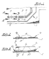
- Figure 1 shows a printed circuit module consisting of a flexible or rigid substrate 1.
- a printed ink layer 2 in the form of conductive traces 9 is printed thereon.
- the conductive traces 9 are separated from each other by intervening non-conductive spaces 3.
- Electronic components 5 are adapted to common the conductive traces 9, and two are shown connecting parallel conductive traces 9.
- Figure 2 is a section of the circuit module, taken along line A-A in Figure 1, showing the two parallel printed conductive traces 9 of printed ink layer 2.
- the conductive traces 9 include contact areas 4 for making an electrical connection to complementary contact surfaces of electronic component 5 or the like.
- Figure 3 is a section of the circuit module, similar to that shown in Figure 2, but taken along line B-B in Figure 1, showing the contact areas 4 of the two parallel printed conductive traces 9.
- An adhesive layer 10 is applied over the contact areas 4 of the conductive traces 9, for example by screen printing.
- Component 5, which includes complementary contact surfaces 6 for electrically connecting to contact areas 4, is fixed to the circuit module with the aid of adhesive 7.
- Adhesive 7 itself is a known plastic-based adhesive used in connecting electronic components to circuit modules and printed circuits.
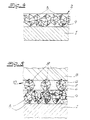
- Figures 4 and 5 depict the portions C and D of Figures 2 and 3, respectively, on a much enlarged scale.
- Figure 4 is an exaggerated depiction of the contact area of the conductive trace imprinted on the circuit module.
- At least the contact areas 4 of the conductive traces 9 of printed ink layer 2 comprise a printable ink with fine conductive crystallites 8 embedded therein, the crystallites being formed of a non-oxidizable crystalline compound of an element of sub-group IV of the Periodic Table, such as titanium, along with nitrogen or carbon.
- the crystallites 8 are distributed in such a way that they are physically touching one another, thus rendering the printed ink layer 2 conductive.
- the preferred embodiment of the invention contemplates that the entire conductive trace 9 comprises such a printed ink layer 2.
- Figure 5 illustrates the four layers of the interface of the printed circuit module and electronic component, including (from the bottom as shown in Figure 5) the printed circuit module 1, the printed ink layer 9, the adhesive layer 10, and the complementary contact surface of the electronic component 5.
- crystallites 8 are also embedded in adhesive 7, formed from an electrically conductive crystalline compound of sub-group IV of the Periodic Table, together with nitrogen or carbon, just like the crystallites within the printed ink layer.
- the adhesive layer 10 the crystallites are distributed therewithin so as not to exhibit any physical contact therebetween, and therefore the adhesive is non-conductive in the direction parallel to its layer plane.
- the non-conductive intervening space 3 between the conductive traces 9 in Figure 2 may also be provided with such adhesive layer 10 by screen printing, since, by virtue of the fact that the adhesive is only conductive in a direction perpendicular to the layer, there will be no conductivity in the area of the intervening spaces.
- the adhesive layer is non-conductive in the layer plane when the number of non-oxidizing crystallites in the adhesive layer is less than 10% by weight.
- contact area 4 or complementary contact surfaces 6 display a protective cover film, or oxide layer, as the crystallites penetrate through such layers.
- the preferred embodiment of the invention contemplates that the thickness of adhesive layer 10 be only slightly more than the thickness of a single crystallite 8. It can also be appreciated from Figure 5 how crystallites 8 are distributed throughout the adhesive in such a way as to exhibit little or no contact with one another so that the adhesive possesses no conductivity along the layer plane.
- Crystallites 8 of printed ink layer 2 and adhesive 7 display relatively equal grain size within a very narrow range.
- crystallites 8 consist of titanium nitride or titanium carbide.
Description
- This invention relates to printed circuit modules, particularly for electronic applications, comprising a rigid or flexible circuit carrier substrate with conductive traces printed thereon adapted for electrically connecting to electronic components.
- Typically, printed circuit modules include conductive traces consisting of a layer of printed ink having fine conductive particles embedded therein. The ink is rendered conductive by physical contact between the conductive particles therewithin, and electronic components are connected to contact areas of the conductive traces to effect an electrical connection therebetween. Such printed circuit modules are used in various areas of electronic technology. The circuit modules can be interchangeable or installed permanently in electronic devices and equipment. Rigid circuit carrier substrates, for example, typically consist of an epoxy resin construction, with glass fiber or glass fiber inserts. Flexible circuit carrier substrates are, for example, films of polyester resin or the like. Electronic components include any components usual in electronics used in conjunction with printed circuits. The electronic components can perform various functions or sophisticated circuitry, and may include functional parts as well as simple junctions or connecting bridges.
- In printed circuit modules known in practice, the conductive traces consist of printed ink layers which include fine metallic particles, such as silver or nickel. However, metallic silver, though very conductive, is not very hard, and both silver and nickel are affected by and corrode under the influence of the surrounding environment. When using such materials, harmful changes in conductivity often cannot be avoided. It is, therefore, usually necessary to coat the conductive traces, and more particularly, the contact areas of the traces, with a protective layer of carbon, for example. However, before the connection of a corresponding contact of an electronic component, the protective layer of carbon must be removed or otherwise be rendered ineffective in order that an adequate electrical connection can be made. These secondary procedures can be time-consuming and costly.
- The document "Database WPI Week 8744, Derwent Publications Ltd.; AN 87-309789 & JP-A-62 217 694" discloses a pressure connection of circuit elements comprising applying electro-conductive particles including carbides, nitrides, borides as an electro-conductive filler to the circuit splice portions. The particles are pressed to the portion through an adhesive layer to form electrical connections with an other element.
- Document "Database WPI Week 8345, Derwent Publications Ltd.; AN 83-812063 & JP-A-58 167 662" discloses a stable conductive adhesive which is mixed with finely powdered titanium carbide and/or titanium nitride in order to achieve a low electric resistance within the adhesive.
- An object of the invention is to provide a printed circuit module having conductive traces with particles embedded therein made from non-oxidizable material wherein the conductivity of the conductive traces is not affected by the environment. Another object of the invention is to provide a simplified connection between the contact surfaces of an electronic component and the contact areas of conductive traces on a printed circuit module. The invention is disclosed in
claims - The invention is characterized in that at least the contact areas of the conductive traces consist of a printed ink layer comprising fine conductive crystallites consisting of a non-oxidizable crystalline compound of an element of sub-group IV of the Periodic Table, for example titanium, along with nitrogen or carbon. Such crystallites are intended to replace the silver or nickel in printing inks, and avoid the costly protective carbon layer for fine pitch traces and contact areas. Preferably the conductive traces themselves consist of such a printed ink layer, that is, the entire trace, including the contact area, may consist of the crystallite-embedded printed ink layer.
- According to another aspect of the invention, making contact between the contact areas of the conductive traces and the corresponding contact surfaces of an electronic component is accomplished whereby the contact surfaces of the electronic component include a hardened adhesive layer, non-conductive along the plane of the layer, in which are embedded the non-oxidizing crystallites formed from a non-oxidizing crystalline compound of an element of sub-group IV of the Periodic Table, such as titanium, together with nitrogen or carbon. The adhesive is a known adhesive used in printed circuit modules having the fine crystallites embedded therein to effect the electrical connection between the two components. The electrical connection is made by pressing down on the electronic component and pressing the crystallites into physical contact with both the contact areas of the conductive traces and the corresponding contact surfaces of the electronic component. The electrical connection is made in a direction perpendicular to the adhesive layer plane, the adhesive being non-conductive in the direction along the layer plane. The adhesive layer is non-conductive in the layer plane when the number of non-oxidizing crystallites in the adhesive layer is less than 10% by weight. The crystallites used in the invention, both in the ink and the adhesive, possess relatively high hardness and are sufficiently sharp-edged to allow being pressed into the contact areas of the conductive traces and into the corresponding contact surfaces of the electronic component. If components are used whose contact surfaces include a protective layer or coating, this is not harmful in the context of the invention, since the crystallites can penetrate the protective layer or layers.
- In the preferred embodiment of the invention, the crystallites consist of titanium nitride, or titanium carbide. Such crystallites possess the requisite hardness and conductivity contemplated by the invention.
- Other objects, features and advantages of the invention will be apparent from the following detailed description, taken in conjunction with the accompanying drawings.
- The invention is explained in detail below by means of the following drawings in which:
- Fig. 1 is a plan view of a printed circuit module which includes a conductive ink layer printed thereon;
- Fig. 2 is a section taken along A-A of the article in Fig. 1, on an enlarged scale;
- Fig. 3 is the section taken along B-B of the article in Fig. 1, on a much enlarged scale;
- Fig. 4 is the portion C in Fig. 2 on a much enlarged scale; and
- Fig. 5 is the portion D in Fig. 3 on the same scale as Fig. 4.
- Figure 1 shows a printed circuit module consisting of a flexible or
rigid substrate 1. A printedink layer 2 in the form ofconductive traces 9 is printed thereon. Theconductive traces 9 are separated from each other by interveningnon-conductive spaces 3.Electronic components 5 are adapted to common theconductive traces 9, and two are shown connecting parallelconductive traces 9. - Figure 2 is a section of the circuit module, taken along line A-A in Figure 1, showing the two parallel printed
conductive traces 9 of printedink layer 2. Theconductive traces 9 includecontact areas 4 for making an electrical connection to complementary contact surfaces ofelectronic component 5 or the like. - Figure 3 is a section of the circuit module, similar to that shown in Figure 2, but taken along line B-B in Figure 1, showing the
contact areas 4 of the two parallel printedconductive traces 9. Anadhesive layer 10 is applied over thecontact areas 4 of theconductive traces 9, for example by screen printing.Component 5, which includes complementary contact surfaces 6 for electrically connecting tocontact areas 4, is fixed to the circuit module with the aid ofadhesive 7.Adhesive 7 itself is a known plastic-based adhesive used in connecting electronic components to circuit modules and printed circuits. - Figures 4 and 5 depict the portions C and D of Figures 2 and 3, respectively, on a much enlarged scale. Figure 4 is an exaggerated depiction of the contact area of the conductive trace imprinted on the circuit module. At least the
contact areas 4 of theconductive traces 9 of printedink layer 2 comprise a printable ink with fineconductive crystallites 8 embedded therein, the crystallites being formed of a non-oxidizable crystalline compound of an element of sub-group IV of the Periodic Table, such as titanium, along with nitrogen or carbon. Thecrystallites 8 are distributed in such a way that they are physically touching one another, thus rendering the printedink layer 2 conductive. The preferred embodiment of the invention contemplates that the entireconductive trace 9 comprises such a printedink layer 2. Figure 5 illustrates the four layers of the interface of the printed circuit module and electronic component, including (from the bottom as shown in Figure 5) theprinted circuit module 1, the printedink layer 9, theadhesive layer 10, and the complementary contact surface of theelectronic component 5. It can be seen in Figure 5 thatcrystallites 8 are also embedded inadhesive 7, formed from an electrically conductive crystalline compound of sub-group IV of the Periodic Table, together with nitrogen or carbon, just like the crystallites within the printed ink layer. However, in theadhesive layer 10, the crystallites are distributed therewithin so as not to exhibit any physical contact therebetween, and therefore the adhesive is non-conductive in the direction parallel to its layer plane. It can be seen that, after applying the compactadhesive layer 10,component 5 is pressed onto theadhesive layer 10, wherebycrystallites 8 are pressed intocontact areas 4 ofconductive traces 9 and complementary contact surfaces 6 ofelectronic component 5, thereby effecting an electrical connection perpendicular to the adhesive layer plane between theconductive traces 9 of the substrate and the electronic component contact surfaces 6. Therefore, the non-conductive interveningspace 3 between theconductive traces 9 in Figure 2 may also be provided with suchadhesive layer 10 by screen printing, since, by virtue of the fact that the adhesive is only conductive in a direction perpendicular to the layer, there will be no conductivity in the area of the intervening spaces. The adhesive layer is non-conductive in the layer plane when the number of non-oxidizing crystallites in the adhesive layer is less than 10% by weight. - It can also be suitable to proceed in the manner described if the
contact area 4 or complementary contact surfaces 6 display a protective cover film, or oxide layer, as the crystallites penetrate through such layers. - As shown in Figure 5, the preferred embodiment of the invention contemplates that the thickness of
adhesive layer 10 be only slightly more than the thickness of asingle crystallite 8. It can also be appreciated from Figure 5 howcrystallites 8 are distributed throughout the adhesive in such a way as to exhibit little or no contact with one another so that the adhesive possesses no conductivity along the layer plane. -
Crystallites 8 of printedink layer 2 and adhesive 7 display relatively equal grain size within a very narrow range. In the preferred embodiment,crystallites 8 consist of titanium nitride or titanium carbide.
Claims (5)
- A printed circuit module for electronic applications includinga circuit substrate (1) having an ink layer (2) printed thereon, the ink layer including electrically conductive traces (9) with contact areas (4) adapted to make an electrical connection with corresponding contact surfaces (6) of an electronic component (5),conductive crystallites (8) embedded therewithin formed from a non-oxidizable crystalline compound of an element of sub-group IV of the Periodic Table, and one of the elements of the group consisting of nitrogen and carbon, andan adhesive layer (10),said crystallites (8) are also distributed in said adhesive layer (10) so as not to exhibit any physical contact therebetween, and, therefore, the adhesive is non-conductive in the direction parallel to its layer plane.
- A printed circuit module for electronic applications includinga circuit substrate (1) having an ink layer (2) printed thereon, the ink layer including electrically conductive traces (9) adapted to make an electrical connection with an electronic component (5),conductive crystallites (8) embedded within the entire printed ink layer (2) formed from a non-oxidizable crystalline compound of an element of sub-group IV of the Periodic Table, and one of the elements of the group consisting of nitrogen and carbon, andan adhesive layer (10),said crystallites (8) are also distributed in said adhesive layer (10) so as not to exhibit any physical contact therebetween, and, therefore, the adhesive is non-conductive in the direction parallel to its layer plane.
- A circuit module as in Claim 1, in which the crystallites consist of titanium nitride.
- A circuit module as in Claim 1, in which the crystallites consist of titanium carbide.
- A circuit module as in Claim 1, wherein the content of the crystallites (8) in the adhesive layer (10) is approximately 10% by weight.
Applications Claiming Priority (2)
| Application Number | Priority Date | Filing Date | Title |
|---|---|---|---|
| DE4209597 | 1992-03-25 | ||
| DE4209597 | 1992-03-25 |
Publications (3)
| Publication Number | Publication Date |
|---|---|
| EP0562571A2 EP0562571A2 (en) | 1993-09-29 |
| EP0562571A3 EP0562571A3 (en) | 1994-02-09 |
| EP0562571B1 true EP0562571B1 (en) | 1996-07-17 |
Family
ID=6454924
Family Applications (1)
| Application Number | Title | Priority Date | Filing Date |
|---|---|---|---|
| EP93104823A Expired - Lifetime EP0562571B1 (en) | 1992-03-25 | 1993-03-24 | Printed circuit module |
Country Status (3)
| Country | Link |
|---|---|
| US (1) | US5340640A (en) |
| EP (1) | EP0562571B1 (en) |
| DE (1) | DE69303645T2 (en) |
Families Citing this family (13)
| Publication number | Priority date | Publication date | Assignee | Title |
|---|---|---|---|---|
| US6271482B1 (en) | 1994-08-23 | 2001-08-07 | Thomas & Betts International, Inc. | Conductive elastomer interconnect |
| US5949029A (en) * | 1994-08-23 | 1999-09-07 | Thomas & Betts International, Inc. | Conductive elastomers and methods for fabricating the same |
| US6580369B1 (en) * | 1995-10-11 | 2003-06-17 | Motorola, Inc. | Electronic tag assembly and method therefor |
| US6881611B1 (en) * | 1996-07-12 | 2005-04-19 | Fujitsu Limited | Method and mold for manufacturing semiconductor device, semiconductor device and method for mounting the device |
| CN1110846C (en) * | 1996-07-12 | 2003-06-04 | 富士通株式会社 | Method and mold for manufacturing semiconductor device, semiconductor device, and method for mounting the device |
| WO1999063794A1 (en) * | 1998-06-02 | 1999-12-09 | Siemens Audiologische Technik Gmbh | A method of mounting a semiconductor die on a printed circuit board |
| WO2002080637A1 (en) | 2001-04-02 | 2002-10-10 | Nashua Corporation | Circuit elements having an embedded conductive trace and methods of manufacture |
| EP1383364A3 (en) * | 2002-05-23 | 2006-01-04 | Nashua Corporation | Circuit elements having an ink receptive coating and a conductive trace and methods of manufacture |
| US6709944B1 (en) * | 2002-09-30 | 2004-03-23 | General Electric Company | Techniques for fabricating a resistor on a flexible base material |
| US20070246158A1 (en) * | 2006-04-21 | 2007-10-25 | 3M Innovative Properties Company | Wiring board, production process thereof and connection method using same |
| US8510935B2 (en) * | 2007-07-10 | 2013-08-20 | Joseph C Fjelstad | Electronic assemblies without solder and methods for their manufacture |
| GB2539684B (en) | 2015-06-24 | 2018-04-04 | Dst Innovations Ltd | Method of surface-mounting components |
| EP3854183A4 (en) * | 2018-09-17 | 2022-06-15 | WestRock MWV, LLC | Circuit assemblies and components thereof for packaging |
Family Cites Families (9)
| Publication number | Priority date | Publication date | Assignee | Title |
|---|---|---|---|---|
| US3875434A (en) * | 1973-10-31 | 1975-04-01 | Du Pont | Pressure-sensitive sensor/logic assembly |
| JPS605077B2 (en) * | 1980-12-19 | 1985-02-08 | 松下電器産業株式会社 | Composition for metallization |
| JPH0240710B2 (en) * | 1982-03-26 | 1990-09-12 | Inoue Japax Res | DODENSEISETSUCHAKUZAI |
| DE3443789A1 (en) * | 1983-12-02 | 1985-06-27 | Osaka Soda Co. Ltd., Osaka | ELECTRICAL CONDUCTIVE ADHESIVE |
| JPS61147593A (en) * | 1984-12-20 | 1986-07-05 | 神東塗料株式会社 | Flexible circuit board with conducting adhesive layer and manufacture thereof |
| JPS6241277A (en) * | 1985-08-16 | 1987-02-23 | Shin Etsu Polymer Co Ltd | Anisotropically conductive adhesive |
| JPS62217694A (en) * | 1986-03-18 | 1987-09-25 | ダイソー株式会社 | Circuit connection |
| JPS62226688A (en) * | 1986-03-27 | 1987-10-05 | 神東塗料株式会社 | Conductive paste compound for bridging |
| US4694572A (en) * | 1986-06-13 | 1987-09-22 | Tektronix, Inc. | Printed polymer circuit board method |
-
1993
- 1993-03-24 US US08/036,309 patent/US5340640A/en not_active Expired - Fee Related
- 1993-03-24 DE DE69303645T patent/DE69303645T2/en not_active Expired - Fee Related
- 1993-03-24 EP EP93104823A patent/EP0562571B1/en not_active Expired - Lifetime
Also Published As
| Publication number | Publication date |
|---|---|
| DE69303645D1 (en) | 1996-08-22 |
| EP0562571A2 (en) | 1993-09-29 |
| US5340640A (en) | 1994-08-23 |
| EP0562571A3 (en) | 1994-02-09 |
| DE69303645T2 (en) | 1997-02-13 |
Similar Documents
| Publication | Publication Date | Title |
|---|---|---|
| EP0562571B1 (en) | Printed circuit module | |
| US5340641A (en) | Electrical overstress pulse protection | |
| EP0329782B1 (en) | Digitizing tablet | |
| EP0400953A2 (en) | Input device | |
| JP4988908B2 (en) | Carrier for land grid array connector | |
| DE3347848C2 (en) | ||
| AU4825090A (en) | Improved method for making printed circuits | |
| GB2170365A (en) | Heat sensitive type adhesive connector | |
| EP0110382A2 (en) | Display device and process for its production and decal for forming a display panel terminal | |
| EP1189271A3 (en) | Wiring boards and mounting of semiconductor devices thereon | |
| EP0782376A3 (en) | Polyimide-metal foil composite film | |
| EP1298967B1 (en) | Electronic card | |
| EP1082882B1 (en) | Method of manufacturing resistors | |
| EP0562569A2 (en) | Anisotropic adhesive for fixing an electronic component to a printed circuit module | |
| KR920005071B1 (en) | Printed circuit board | |
| US4934470A (en) | Data input board | |
| EP0307007A3 (en) | Making electrical contact between metals and resistive emaking electrical contact between metals and resistive elements lements | |
| EP0605689B1 (en) | Anisotropic electrical connection | |
| JPS5951110B2 (en) | Light-receiving type display substrate | |
| JPH0524633B2 (en) | ||
| US6903561B2 (en) | Circuitry for measuring mechanical stress impressed on a printed circuit board | |
| GB2186745A (en) | Mounting electronic devices | |
| EP0215953A1 (en) | Film connector and method of manufacturing same | |
| JPS62128591A (en) | Solid molded product which has printed wiring on the surface | |
| JPS59119891A (en) | Circuit board |
Legal Events
| Date | Code | Title | Description |
|---|---|---|---|
| PUAI | Public reference made under article 153(3) epc to a published international application that has entered the european phase |
Free format text: ORIGINAL CODE: 0009012 |
|
| AK | Designated contracting states |
Kind code of ref document: A2 Designated state(s): DE FR GB IT |
|
| PUAL | Search report despatched |
Free format text: ORIGINAL CODE: 0009013 |
|
| AK | Designated contracting states |
Kind code of ref document: A3 Designated state(s): DE FR GB IT |
|
| 17P | Request for examination filed |
Effective date: 19940730 |
|
| 17Q | First examination report despatched |
Effective date: 19941216 |
|
| ITF | It: translation for a ep patent filed |
Owner name: DE DOMINICIS & MAYER S.R.L. |
|
| GRAH | Despatch of communication of intention to grant a patent |
Free format text: ORIGINAL CODE: EPIDOS IGRA |
|
| GRAA | (expected) grant |
Free format text: ORIGINAL CODE: 0009210 |
|
| AK | Designated contracting states |
Kind code of ref document: B1 Designated state(s): DE FR GB IT |
|
| REF | Corresponds to: |
Ref document number: 69303645 Country of ref document: DE Date of ref document: 19960822 |
|
| ET | Fr: translation filed | ||
| PLBE | No opposition filed within time limit |
Free format text: ORIGINAL CODE: 0009261 |
|
| STAA | Information on the status of an ep patent application or granted ep patent |
Free format text: STATUS: NO OPPOSITION FILED WITHIN TIME LIMIT |
|
| 26N | No opposition filed | ||
| PGFP | Annual fee paid to national office [announced via postgrant information from national office to epo] |
Ref country code: GB Payment date: 20010202 Year of fee payment: 9 |
|
| PGFP | Annual fee paid to national office [announced via postgrant information from national office to epo] |
Ref country code: FR Payment date: 20010301 Year of fee payment: 9 |
|
| PGFP | Annual fee paid to national office [announced via postgrant information from national office to epo] |
Ref country code: DE Payment date: 20010330 Year of fee payment: 9 |
|
| REG | Reference to a national code |
Ref country code: GB Ref legal event code: IF02 |
|
| PG25 | Lapsed in a contracting state [announced via postgrant information from national office to epo] |
Ref country code: GB Free format text: LAPSE BECAUSE OF NON-PAYMENT OF DUE FEES Effective date: 20020324 |
|
| PG25 | Lapsed in a contracting state [announced via postgrant information from national office to epo] |
Ref country code: DE Free format text: LAPSE BECAUSE OF NON-PAYMENT OF DUE FEES Effective date: 20021001 |
|
| GBPC | Gb: european patent ceased through non-payment of renewal fee |
Effective date: 20020324 |
|
| PG25 | Lapsed in a contracting state [announced via postgrant information from national office to epo] |
Ref country code: FR Free format text: LAPSE BECAUSE OF NON-PAYMENT OF DUE FEES Effective date: 20021129 |
|
| REG | Reference to a national code |
Ref country code: FR Ref legal event code: ST |
|
| PG25 | Lapsed in a contracting state [announced via postgrant information from national office to epo] |
Ref country code: IT Free format text: LAPSE BECAUSE OF NON-PAYMENT OF DUE FEES;WARNING: LAPSES OF ITALIAN PATENTS WITH EFFECTIVE DATE BEFORE 2007 MAY HAVE OCCURRED AT ANY TIME BEFORE 2007. THE CORRECT EFFECTIVE DATE MAY BE DIFFERENT FROM THE ONE RECORDED. Effective date: 20050324 |