EP0558034B1 - Digitaler Demodulator für TT/4-QPSK-Signale - Google Patents
Digitaler Demodulator für TT/4-QPSK-Signale Download PDFInfo
- Publication number
- EP0558034B1 EP0558034B1 EP93103054A EP93103054A EP0558034B1 EP 0558034 B1 EP0558034 B1 EP 0558034B1 EP 93103054 A EP93103054 A EP 93103054A EP 93103054 A EP93103054 A EP 93103054A EP 0558034 B1 EP0558034 B1 EP 0558034B1
- Authority
- EP
- European Patent Office
- Prior art keywords
- signal
- decision
- phase
- sampling
- decision error
- Prior art date
- Legal status (The legal status is an assumption and is not a legal conclusion. Google has not performed a legal analysis and makes no representation as to the accuracy of the status listed.)
- Expired - Lifetime
Links
Images


Classifications
-
- H—ELECTRICITY
- H04—ELECTRIC COMMUNICATION TECHNIQUE
- H04L—TRANSMISSION OF DIGITAL INFORMATION, e.g. TELEGRAPHIC COMMUNICATION
- H04L27/00—Modulated-carrier systems
- H04L27/18—Phase-modulated carrier systems, i.e. using phase-shift keying
- H04L27/22—Demodulator circuits; Receiver circuits
- H04L27/233—Demodulator circuits; Receiver circuits using non-coherent demodulation
- H04L27/2335—Demodulator circuits; Receiver circuits using non-coherent demodulation using temporal properties of the received signal
- H04L27/2337—Demodulator circuits; Receiver circuits using non-coherent demodulation using temporal properties of the received signal using digital techniques to measure the time between zero-crossings
Definitions
- the present invention relates to a data demodulator for reproducing digital data from receive signals which have undergone differential phase-shift-keying (DPSK), and more particularly to a data demodulator wholly consisting of digital circuits, well suitable for digital cellular telecommunication systems of an M-channel (M is a positive integer) multiplex time division multi-access (TDMA) formula.
- DPSK differential phase-shift-keying
- ⁇ /4-shift quadrature phase-shift-keyed ( ⁇ /4QPSK) signals in transmission and reception between the radio base station and any mobile unit (for instance according to "RCR Standards on Digital Cellular Telecommunication Systems", RCR STD-27A, Jan. 1992, Research & Development Center for Radio Systems).
- a data demodulator for DPSK signals should correct frequency drifts (or frequency offsets) of receive signals while achieving appropriate synchronization, and thereby improve the error rate of the demodulated data.
- a data demodulator for use in a TDMA system should quickly achieve symbol synchronization of burst signals, correct their frequency drifts and, where continuous reception takes place, accomplish said symbol synchronization and frequency drift correction taking account of resistance to noise and other pertinent factors.
- the aforementioned ACT type data demodulator controls the frequency and phase of said reference signal independently of each other with an ACT circuit, an automatic frequency control (AFC) circuit and a phase/frequency control circuit to correct the carrier phase rotation of the ⁇ /4 QPSK signals on a symbol-by-symbol basis.
- This data demodulator because it controls the frequency drifts of the ⁇ /4 QPSK signals relative to the reference signal and the reference phase for phase detection independently of each other, is quick in responding to burst signals such as TDMA signals, but has no function to optimize symbol synchronism.
- This data demodulator moreover, requires more or less complex circuits for controlling the phase and frequency, such as said ACT circuit, AFC circuit and phase/frequency control circuit.
- US-A-4,849,991 discloses a DPSK data demodulator which extracts proper symbol timing of the TDMA signal when the TDMA signal is taken as a whole.
- a first object of the present invention is to provide a fully digitized data demodulator for differential phase-shift-keyed (DPSK) signals, readily permitting large scale integration (LSI) and dispensing with adjustment.
- DPSK differential phase-shift-keyed
- LSI large scale integration
- the demodulator according to the invention suitable for the reception of TDMA signals comprises means for optimal adjustment of the symbol synchronism phase of demodulated data and means to correct the frequency drifts of receive signals, permits the realization of said symbol synchronizing means and frequency drift correction means in simple configurations, and is capable of flexibly varying the quantity of the setting of said symbol synchronism phase and that of said frequency drift correction according to the state of receive signals.
- a data demodulator subjects DPSK-modulated TDMA signals to delayed detection by phase detection means, delay means and phase difference detection means connected in cascade to generate phase difference signals synchronized with N-phase clock signals. These phase difference signals are reproduced into decision data by decision means.
- this data demodulator obtains symbol-synchronized demodulated data by sampling said decision data with the optimal one among N sampling phases.
- This data demodulator is characteristic in the method of selecting said optimal sampling phase.
- First sampling phase calculating means adds for a prescribed period a decision error signal based on the difference between said phase difference signal and decision data every time said N-phase clock signal is entered, and selects as said sampling phase the phase of the clock signal corresponding to the signal indicating the smallest value among the added N decision error signals.
- Second sampling phase calculating means weights the adding method of said decision error signals according to the reception state of the TDMA signals.
- One of the ways it is weighted is to subject the sampling phase obtained from a preceding TDMA burst and a newly obtained sampling phase to weighted averaging to give a normal sampling phase.
- this data demodulator is provided, between said phase difference detection means and said decision means, with subtraction means for subtracting a correcting value from said phase difference signal to eliminate the D.C. offset of said phase difference signal due to the frequency drift of the receive signal.
- This data demodulator is characteristic in the method of calculating said correcting value.
- First correcting value calculating means calculates the average of decision error signals based on the differences between said phase difference signals and decision data during a certain period, and provides this average as said correcting value.
- Second correcting value calculating means weights the method of calculating said correcting value according to the reception state of the TDMA signals. One of the ways it is weighted is to take into account a correcting value obtained from a preceding TDMA burst in the calculation of said correcting value.
- this data demodulator constitutes part of the base station apparatus of a digital cellular telecommunication system of a TDMA formula.
- This base station apparatus includes a transmitter unit (not shown) for transmitting M-channel TDMA signals, a receiver unit (not shown) for receiving ⁇ /4 QPSK signals of the 800 MHz band transmitted over a designated channel among the M TDMA signal channels, and a control unit (not shown) for controlling said transmitter unit and receiver unit.
- the high frequency section of said receiver unit converts the received ⁇ /4 QPSK signals into receive signals r of an intermediate frequency (455 kHz, for instance) band.
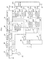
- the data demodulator receives this ⁇ /4QPSK-modulated receive signals r at an input terminal 100.
- the data demodulator wholly consisting of digital circuits, includes phase detector 101, delay circuit 102, phase difference detector 103, decision circuit 104, and reference signal generator or oscillator 105 for generating a reference signal fr of a frequency substantially equal to K (K is a positive integer) times the center frequency of the receive signal r , all known means to persons skilled in the art.
- the phase detector 101 shapes the waveform of the receive signal r from the input terminal 100 to a logic level, and detects the phase of the receive signal r by comparing the zero cross point of this wave-shaped receive signal r and that of a signal resulting from the frequency division of the reference signal fr by K.
- the phase detector 101 further samples this detected phase N times per symbol (period Ts) of the receive signal r with N-phase (N is a positive integer) clock signals clk , i.e. c1 , ..., cN , from a timing signal generator 106A, and gives this sampled detected phase as the phase signal p1 of the receive signal r .
- N-phase clock signals clk i.e. c1 , ..., cN
- the phase detector 101 outputs N-phase signals p1 per symbol in numerical data in a parallel form in response to the receive signal r , the reference signal fr and the clock signals clk .
- the accuracy of the phase detection of the receive signal r by the phase detector is 2 ⁇ /K radians.
- the phase signal p1 is supplied to the delay circuit 102, which generates a delayed phase signal p2 by delaying the phase signal p1 by one symbol.
- the phase difference signal p3 is the difference between the phase signal p1 earlier by one symbol (the delayed phase signal p2 ) and a newly received phase signal p1 , i.e. a signal resulting from delayed detection of a ⁇ /4 QPSK-modulated receive signal r .
- the decision circuit 104 compares the phase difference signal p3 with a predetermined value, and generates decision data d1 of a two-column four-value signal (see FIG. 2). Thus, the decision circuit 104 determines which of four ranges including (- ⁇ to - ⁇ /2) , (- ⁇ /2 to 0), (0 to ⁇ /2) and ( ⁇ /2 to ⁇ ) the phase difference signal p3 belongs to, and generates decision data d1 corresponding to the defined range, i.e. (1, 1), (1, 0), (0, 0) or (0, 1).
- N pairs of decision data d1 are generated per symbol of the receive signal r .
- timing signal generator 106 receives frame signal f from the control unit of said base station apparatus every time the receive TDMA channel (frame) is switched (times t2 and t6), and generates a channel number indicating signal ch synchronized with the frame signal f, a clock signal clk , a clear signal clr and a sampling signal load (see FIG. 3).
- the timing signal generator 106 generates the clock signal clk beginning at the switching times t2 and t6 of the TDMA channel, the channel number indicating signal ch upon reception of the frame signal f , the sampling signal load at the final ones of the reception timing for a specific TDMA channel (times t1 and t5), and the clear signal clr immediately after the generation of the sampling signal (times t2 and t6).
- the timing signal generator 106 does not generate the channel number indicating signal ch , but generates the sampling signal load and the clear signal clr in prescribed periods, here in the same frame periods Tf as when the receive signals r are M-channel TDMA signals.
- Decision error squaring circuit 112 generates the square ea of the decision error in response to the N-phase phase difference signal p3 and the decision data d1 (see FIG. 2).
- the squares of the differences between decision phases -3 ⁇ /4, - ⁇ /4, ⁇ /4 and 3 ⁇ /4 radians respectively corresponding to the decision data d1 (1, 1), (1, 0), (0, 0) and (0, 1) and the phase represented by the phase signal p3 are obtained at the output of the circuit 112 in the relationship of correspondence shown in FIG. 2.
- the decision circuit 104 decides which of the two ranges (- ⁇ to 0) and (0 to ⁇ ) the phase difference signal p3 belongs to, and generates a decision datum d1 corresponding to that range, i.e. (1) or (0). Therefore, the decision phase corresponding to the decision data d1 of the ⁇ /2-shifted BPSK signal are - ⁇ /2 and ⁇ /2 radians.
- Each of N square error adders 113-1, ..., 113-N adds the square ea of the decision error every time a clock signal c1 , ..., or cN of the corresponding phase is entered to generate decision error sums ea1 , ..., eaN , and clears the decision error sums ea1 , ..., eaN upon inputting of the clear signal clr .
- the decision error sums ea1 , ..., eaN are stored into square error registers 115-1, ..., 115-N, which sample the decision error sums ea1 , ..., eaN at the timing of the sampling signal load (time t1), and supply the sampled decision error sums es1 , ..., esN to signal processing means 107A.
- the data generated by the square error adders 113-1, ..., 113-N are acceptable if they are based on the decision errors ( p1 - d1 ) in the different phases of the clock signals clk . Therefore, the decision error squaring means 112 may be replaced with decision error detection means generating the absolute values of the decision errors ( p1 - d1 ).
- the signal processing means 107A responds to the decision error sums es1 , ..., esN which have been read out and to reception information inf from said control unit, and calculates a sampling phase signal s1 by a sampling phase calculating technique to be described below.
- This sampling phase signal s1 which is instructing information to have signal sampling means 111 sample the decision data d1 in a selected phase of the clock signal clk , indicates the phase number of the clock signal clk .
- the signal processor 107A writes the sampling phase signal s1 into a sampling phase register 114-1.
- the signal sampling circuit 111 samples the decision data d1 at a timing (in a phase) instructed by a clock signal clk and the sampling phase signal s1 from the phase register 114-1, and generates at an output terminal 200 demodulated data d2 at a symbol rate resulting from the optimizing adjustment of the symbol synchronism phase.
- the symbol synchronism timing of the demodulated data d2 is the second phase of the clock signal clk (times t3 and t4).
- the data demodulator for demodulating M-channel TDMA signals is provided with M sampling phase registers 114-1, ..., 114-M corresponding to the number of channels, M.
- the signal processor 107A calculates a sampling phase number sj ( j is an integer neither smaller than 1 nor greater than M) in response to the decision error sums es1 , ..., esN read out at every timing of reception end and to the receive information inf , and writes this sampling phase signal sj into the sampling phase register 114-j for the j th channel.
- the sampling phase registers 114-1, ..., 114-M write sampling phase signals s1 , ..., sM of the respectively corresponding TDMA channels.
- the signal sampling circuit 111 samples the decision data d1 at the sampling timing indicated by the sampling phase channel sj corresponding to the channel number indicating signal ch and by a clock signal clk .
- the TDMA channel “1" in FIG. 3 indicates the symbol synchronism timings of the demodulated data d2 when "2" is written in the phase register 114-1 (times t3 and t4), and the TDMA channel "2" shows the symbol synchronism timing of the demodulated data d2 when "N" is written in the phase register 114-N (time t7).
- the input/output (I/O) port 202 of the signal processor 107A reads out the decision error sums es1 , ..., esN from the square error registers 115-1, ..., 115-N, respectively, upon completion on every TDMA channel.
- These decision error sums es1 , ..., esN are separately stored in N x M decision error storing memories 205.
- a microprocessor (CPU) 201 computes the optimal sampling phase signal sj for each TDMA channel in response to one or another of these decision error sums es1 , ..., esN , and writes this sampling phase signal sj into the sampling phase register 114-j for the corresponding TDMA channel via the I/O port 202.
- the CPU 201 operates in accordance with a program stored in a program ROM 203.
- One of the techniques to compute the optimal sampling phase signal sj for the decision data d1 is suitable for use when it is desired to subject a receive signal r in a burst state (burst signal) to symbol synchronization upon start of reception.
- the square error registers 115-1, ..., 115-N sample the decision error sums es1 , ..., esN , respectively
- the signal processor 107A reads out these decision error sums es1 , ..., esN to find out the smallest decision error sum esi .
- the timing of the clock signal clk for the square error register 115-8 to give this smallest sum esi i.e. the phase of the i th phase clock signal ci , is selected as the optimal sampling phase for the decision data d1 .
- This method to compute the optimal sampling phase signal si is applicable irrespective of whether the number of TDMA channel(s) is one or more.
- Another technique to compute the optimal sampling phase si is suitable for use when the receive signal r is a TDMA signal. This is based on the fact that the drift of the optimal sampling phase signal si is extremely small between burst signals in which TDMA signals of the same channel adjoin one another.
- the signal processor 107A finds out a new sampling phase signal si by subjecting the past sampling phase values si and a newly computed sampling phase signal si to weighted averaging instead of computing an entirely new optimal sampling phase signal si for each sample of the decision error sums es1 , ..., esN .
- the signal processor 107A computes a weighted average decision error wesi for each of the first to the Nth phases by Equation (1), and selects as the new sampling phase signal si the phase of the clock signal ci of the square error register 115-i which gives the smallest value of this weighted average decision error wesi .
- wesi ⁇ ⁇ (decision error sum esi ⁇ ) ⁇ w + (value stored in decision error storing memory 205) ⁇ (1 - w) ⁇ where 0 ⁇ the weighting coefficient w ⁇ 1.
- the greater the weighting coefficient w the sooner the symbol synchronization. Therefore, the value of the weighting coefficient w is set greater immediately after the start of reception of receive signals r on a given channel and, after completion of the synchronization, it is reduced to a smaller value to restrain fluctuations due to noise superimposed on the receive signals r .
- the square error memories 205 are cleared and, when the reception of receive signals r is to begin, the sampling phase signal si is determined solely on the basis of the value of the square error register 115-i. As a result, the symbol synchronization of burst signals r with short preambles is accelerated in this data demodulator.
- the CPU 201 varies the weighting coefficient w in response to the receive information inf notifying the state of the reception of said receive signals r from said control unit and to the software program of the program ROM 203.
- the signal processor 107A since it is undesirable to let the square error memories 205 to be cleared by any instantaneous interruption of the receive signal r , the signal processor 107A requires protecting means to prevent the square error memories 205 from being cleared and the sampling phase signal si from varying abruptly in time of instantaneous interruption of the receive signal r .
- said receiver apparatus detects the receive field intensity of the ⁇ /4 QPSK signals received and, if this receive field intensity is above a prescribed level, will supply the receive information inf to the signal processor 107 via said control unit.
- the receive signals r include any sync signal
- sync signal detecting means known to those skilled in the art will transmit the receive information inf upon detection of said sync signal.
- the receive signals r are in the form of error detection codes
- the error detecting means of said receiver unit will transmit the receive information inf upon detection of said error detection codes.
- said control unit will transmit the receive information inf upon detection of a signal expected in advance.
- said radio apparatus can use a suitable one of them for this data demodulator to supply the receive information inf to the signal processor 107A.
- this flow chart shows the second technique for computing the sampling phase.
- the CPU 201 reads out decision errors es1 , ..., esN from the square error registers 115-1, ..., 115-N, respectively, at the time of reception end on a certain TDMA channel (t1 if its is the Mth channel) (step 11).
- the CPU 201 further reads out the contents of the decision error storing memories 205 corresponding to these decision errors es1 , ..., esN (M-1, ..., M-N if it is the Mth channel), computes the weighted average decision errors wes1 , ..., wesN by Equation (1), and stores these weighted average decision errors wes1 , ..., wesN into the decision error storing memories 205 (M-1, ..., m-N) (step 12).
- the CPU 201 then computes the sampling phase signal si ( sM if it is the Mth channel) corresponding to the smallest value of the weighted average decision errors wes1 , ..., wesN (step 13).
- the CPU 201 stores the computed sampling phase signal si into the sampling phase register 114-j (114-M if it is the Mth channel) (step 14). This flow of sampling phase computation is repeated for each channel of the TDMA signals.
- a signal selector 253 of this signal sampling circuit 111 selects one of the M sampling phase signals s1, ..., sM as designated by the channel number indicating signal ch . Since the first through Mth channels are used in repeated cycles for the TDMA signals, the signal selector 253, every time the channel number indicating signal ch is entered, selects the sampling phase signal sj for the next channel (supposed to be j th channel) following modulo M. This sampling phase signal sj is used as the control signal for another signal selector 252.
- the signal selector 252 selects one of N clock signals clk ( c1 , ..., cN ), ci in this case, according to the phase number i indicated by the sampling phase signal sj .
- a sampling circuit 251 samples the decision data d1 with the phase of the clock signal ci selected as the optimal sampling phase, and generates demodulated data d2 of the symbol rate.
- the data demodulator which is the preferred embodiment illustrated in FIG. 1, readily permits large scale integration and dispenses with adjustment because it wholly consists of digital circuits. As it optimizes the symbol synchronism phase for every channel of TDMA signals, demodulated data d2 with the least error rate can be obtained for each channel. Furthermore this data demodulator, which flexibly various the technique to set the sampling phase signal si for the decision data d1 according to the contents of receive signals r , can achieve quick symbol synchronization at the time of starting the reception of burst signals and, at the same time, realize the reproduction of data with less errors in consecutive reception on the same TDMA channel even if the the receive signals r are accompanied by much noise.
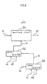
- a data demodulator illustrated in this drawing which is another preferred embodiment of the present invention, like the one shown in FIG. 1, includes phase detector 101 for receiving a receive signal r having undergone ⁇ /4 QPSK modulation from an input terminal 100, delay circuit 102, phase difference detector 103, decision circuit 104, reference signal generator 105 for generating a reference signal fr , and timing signal generator 106.
- This data demodulator further includes subtraction circuit 121 arranged between the phase difference detector 103 and the decision circuit 104, and signal processor 107B, which is substantially similar to its counterpart in the embodiment shown in FIG. 1.
- the signal processor 107B though having the same constituent elements as the signal processor 107A, is different in the way it processes signals as will be described below.
- a phase difference signal p3 will have a D.C. offset. If this phase difference signal p3 having a D.C. offset is directly supplied to the decision circuit 104, the decision circuit 104 will generate decision data d1 with many errors due to the D.C. offset. To eliminate this disadvantage, the subtraction circuit 121 subtracts from the phase difference signal p3 a correction value pr for the frequency drift, and thereby generates a corrected phase difference signal p4 cleared of the D.C. offset due to the frequency drift. This corrected phase difference signal p4 is supplied to the decision circuit 104, which generates decision data d1 whose data errors due to said frequency drift have been reduced.
- decision error detector 122 generates a decision error eb in response to the corrected phase difference signal p4 and the decision data d1 .
- the decision phases corresponding to the decision data d1 (1, 1), (1, 0), (0, 0) and (0, 1) are -3 ⁇ /4, - ⁇ /4, ⁇ /4 and 3 ⁇ /4 radians, respectively.
- decision error adding means 124 generates a decision error sum eb1 by adding a decision error eb every time a clock signal clk N times the symbol rate, i.e. having N phases, is entered, and clears the decision error sum eb1 at a timing before the start of reception on each TDMA channel (time t2 for channel "1" and time t6 for channel “2”) in response to a clear signal clr .
- the period during which the decision error signals eb are added is one TDMA frame period (period Tf ).
- the decision error sum eb1 is supplied to a decision error register 126, which samples the decision error sum eb1 at the timings of a sampling signal load (times t1 and t2), and supplies the sampled decision error sum eb2 to the signal processor 107B.
- the signal processor 107B computes frequency drift correction values pr1 , ..., prM for each TDMA channel of the receive signals r as will be described below in response to a decision error sum es3 that has been read out and to receive information inf , and writes these correction values pr1 , ..., prM into respectively corresponding correction data registers 125-1, ..., 125-M.
- a signal selector 123 selects the correction data register 125-j of the j th channel indicated by a channel number indicating signal ch , and supplies the subtraction circuit 121 with the correction value prj stored in the correction data register 125-j as the correction value pr .
- the signal processor 107B reads out, every time the decision error register 126 samples the decision error sum eb2, this decision error sum eb2 , and computes the average prj of the decision errors eb on this channel (supposed to be the j th channel) in every fixed period, which is one frame period Tf of TDMA signals here. Where one frame period Tf consists of H symbols, the decision error eb is added N x H times, and the average prj is represented by Equation (2).
- the value prj which is the average of decision errors eb on this j th channel, represents the D.C. offset quantity of the phase difference signal p4 . If this average prj is obtained on, for instance, the Mth channel, the correction value prM currently set for the Mth channel will be deviating from the proper correction value by the average prj . Therefore, the signal processor 107B adds this average prj to the correction value prM stored in the correction data register 125-M for the M-th channel as indicated by Formula (3), and writes the sum of this addition into the correction data register 125-M as a new correction value prM . prM ⁇ ⁇ prM ⁇ + eb2 ⁇ /(N ⁇ H)
- the corrected phase difference signal p4 on the Mth TDMA channel will thereafter have no D.C. offset, and the Mth channel will be cleared of the impact of the frequency drift.
- the greater the value of the weighting coefficient v the shorter the period of frequency drift correction. Therefore, immediately after the start of receiving burst signals r , the value of the weighting coefficient v is set greater, and it is reduced to a smaller value after the completion of frequency drift correction, when the correction value prM becomes smaller than a prescribed level, to restrain the fluctuations of the correction value prM due to receiver noise.
- the weighting coefficient to 1 at the time of receiving the first burst signal r (the same as by the first correction value computing technique)
- the frequency drift can be immediately corrected.
- the signal processor 107B since it is undesirable to let the decision error memories 205 to be cleared by any instantaneous interruption of the receive signal r , the signal processor 107B requires protecting means to prevent the decision error memories 205 from being cleared and the correction value pr from varying abruptly in time of instantaneous interruption of the receive signal r .
- the flow chart of this figure shows the second technique for correction value computation.
- the signal processor 107B reads out the decision error sum eb2 from the decision error register 126 at t1, the ending time of TDMA signals on the Mth channel (step 21).
- the signal processor 107B then reads the Mth channel correction value prM corresponding to the decision error eb2 from the correction data register 125-M, and computes a new correction value prM by Formula (4), using the read-out correction value prM , the decision error sum eb2 and the weighting coefficient v (or v1 ) which has been prepared in response to the receive information inf and varies over time (step 22).
- the signal processor 107B stores the new correction value prM into the correction data register 125-M (step 23). The flow described so far is repeated in the reception of TDMA signals on every channel.
- data demodulators readily permit large scale integration and dispense with adjustment because all their circuits including symbol synchronization circuits or frequency drift correcting circuits are digitized. Since these data demodulators flexibly vary the setting of the phase adjustment parameter for symbol synthronism and the correction parameter for frequency drift correction with the signal processor 107A and 107B and by a plurality of computing techniques including the varying of the weighting coefficients w and v over time according to the reception state of receive signals r , they have the characteristic of being able not only to promptly achieve said symbol synchronization and correct any frequency drift into a normal reception state on every TDMA channel but also to reproduce demodulated data in a normal reception state with a low error rate even in the presence of much noise.
Landscapes
- Engineering & Computer Science (AREA)
- Computer Networks & Wireless Communication (AREA)
- Signal Processing (AREA)
- Digital Transmission Methods That Use Modulated Carrier Waves (AREA)
Claims (19)
- Datendemodulator mit:einer Phasendetektionseinrichtung (101) zum Detektieren der Phase eines Empfangssignals (r), das eine Phasendifferenzumtastung (DPSK) erfahren hat, durch Vergleichen der Phase des Empfangssignals und der eines Referenzsignals (fr), dessen Frequenz im wesentlichen gleich dem K-fachen (K ist eine positive Ganzzahl) der Mittenfrequenz des Empfangssignals (r) ist, und Abtasten der Phase des Empfangssignals, die detektiert wurde, um ein Phasensignal in einer parallelen Signal form bei jeder Zuführung eines Taktsignals, das aus der Teilung der Symbolperiode des Empfangssignals in N Phasen (N ist eine positive Ganzzahl) resultiert, zu ergeben;einer Verzögerungseinrichtung (102) zum Erzeugen eines verzögerten Phasensignals durch Verzögern des Phasensignals um ein Symbol;einer Phasendifferenz-Detektionseinrichtung (103) zum Erzeugen eines Phasendifferenzsignals durch Subtrahieren des verzögerten Phasensignals von dem Phasensignal; einer Entscheidungseinrichtung (104), die auf ein korrigiertes Phasendifferenzsignal zum Erzeugen von Entscheidungsdaten (dl) reagiert, die das Ergebnis der Phasenentscheidung des Phasendifferenzsignals sind;wobei die Empfangssignale M-Kanal-TDMA-Signale (M ist eine positive Ganzzahl) sind;
ferner mit:einer Entscheidungsfehler-Berechnungseinrichtung (122), die auf das korrigierte Phasendifferenzsignal (p4) und die Entscheidungsdaten (dl) reagiert, zum Berechnen eines Entscheidungsfehlers (eb) auf der Grundlage der Differenz zwischen der Phase des korrigierten Phasendifferenzsignals (p4) und der Entscheidungsphase der Entscheidungsdaten (d1);N Entscheidungsfehler-Addiereinrichtungen (124), jeweils zum Erzeugen einer Entscheidungsfehlersumme (eb1) durch Addieren des Entscheidungsfehlers (eb) bei jeder Zuführung eines Taktsignals der entsprechenden Phase und zum Löschen der Entscheidungsfehlersumme (eb1) als Reaktion auf ein Löschsignal;N Entscheidungsfehlerregistern (126), jeweils zum Speichern der Entscheidungsfehlersumme von der entsprechenden der Entscheidungsfehler-Addiereinrichtungen (124) bei jeder Zuführung eines Abtastsignals;M Abtastphasenregistern (114-1 bis 114-M) zum Speichern eines Abtastphasensignals für jeden der Kanäle;einer Abtasteinrichtung zum Erzeugen von symbolratendemodulierten Daten durch Abtasten der Entscheidungsdaten in einer Phase, die durch das Taktsignal, die M Abtastphasensignale und ein Kanalnummer-Anzeigesignal (ch) angezeigt ist; undeiner Signalverarbeitungseinrichtung (107B), ferner mit einer Leseeinrichtung zum Auslesen der Entscheidungsfehlersumme für jeden der Kanäle aus jedem der N Entscheidungsfehlerregister, einer Abtastphasen-Berechnungseinrichtung, die auf jede dieser Entscheidungsfehlersummen reagiert, zum Berechnen des Abtastphasensignals für jeden Kanal durch eine vorgeschriebene Berechnungstechnik und einer Speichereinrichtung zum Speichern jedes der Abtastphasensignale in einem oder einem anderen der M Abtastphasenregister;gekennzeichnet durch:eine Subtrahiereinrichtung (121), die zwischen der Phasendifferenz-Detektionseinrichtung (103) und der Entscheidungseinrichtung (104) eingefügt ist, zum Subtrahieren eines Korrekturwerts von dem durch die Phasendifferenz-Detektionseinrichtung (103) erzeugten Phasendifferenzsignal (p3) zum Korrigieren des Gleichstromversatzes dieses Phasendifferenzsignals und Zuführen des korrigierten Phasendifferenzsignals (p4) zu der Entscheidungseinrichtung (104); undM Korrekturregister (125-1 bis 125-M) zum Speichern des Korrekturwerts für jeden entsprechenden TDMA-Kanal der Empfangssignale. - Datendemodulator nach Anspruch 1, wobei das Empfangssignal eine Quadratur-Phasenumtastung mit π/4-Verschiebung (π/4-QPSK) erfahren hat.
- Datendemodulator nach Anspruch 1 oder 2, wobei die Entscheidungsfehler-Berechnungseinrichtung (122) eine Entscheidungsfehler-Quadriereinrichtung zum Erzeugen des Entscheidungsfehlers durch Quadrieren der Differenz zwischen der Phase des Phasendifferenzsignals und der Entscheidungsphase der Entscheidungsdaten ist.
- Datendemodulator nach Anspruch 1 oder 2, wobei die Entscheidungsfehler-Berechnungseinrichtung (122) eine Absolutwert-Berechnungseinrichtung zum Erzeugen des Entscheidungsfehlers durch Berechnen des Absolutwerts der Differenz zwischen der Phase des Phasendifferenzsignals und der Entscheidungsphase der Entscheidungsdaten ist.
- Datendemodulator nach einem der Ansprüche 1 bis 4, ferner mit einer Taktungssignal-Erzeugungseinrichtung (106), die ein Rahmensignal (f) als Meldung der TDMA-Kanalumschaltung des Empfangssignals empfängt, zum Erzeugen des Taktsignals (clk), das mit diesem Rahmensignal (f) synchronisiert ist, des Abtastsignals (load), des Löschsignals (clr) und des Kanalnummer-Anzeigesignals (ch).
- Datendemodulator nach Anspruch 5, wobei:das Abtastsignal (load) unmittelbar vor dem Empfangsende des Empfangssignals auf jedem TDMA-Kanal vorbereitet wird;das Löschsignal (clr) zwischen der Vorbereitung des Abtastsignals und dem Empfang des Rahmensignals vorbereitet wird; unddas Kanalnummer-Anzeigesignal (ch) nach Empfang des Rahmensignals (f) vorbereitet wird.
- Datendemodulator nach Anspruch 6, wobei die Signalverarbeitungseinrichtung (107B) ferner aufweist:eine Eingabe/Ausgabe-(E/A-)Einrichtung (202) zum Auslesen der Entscheidungsfehlersumme aus jedem der N Entscheidungsfehlerregister bei jeder Zuführung des Abtastsignals und Einschreiben des Abtastphasensignals in das Abtastphasenregister für den entsprechenden Kanal, undeine Berechnungseinrichtung (201), die auf die N Entscheidungsfehlersummen reagiert, die ausgelesen wurden, zum Senden einer der Phasen des Taktsignals zu der E/A-Einrichtung als das Abtastphasensignal.
- Datendemodulator nach Anspruch 6 oder 7, wobei die Abtastphasen-Berechnungseinrichtung die Taktsignalphase, die dem kleinsten Wert der Entscheidungsfehlersumme entspricht, als das Abtastphasensignal sendet.
- Datendemodulator nach Anspruch 7 oder 8, wobei die E/A-Einrichtung (202) ferner Empfangsinformationen als Anzeige des Empfangszustands des Empfangssignals empfängt, und
die Berechnungseinrichtung (201) ferner auf die Empfangsinformationen reagiert, um die Entscheidungsfehlersummen mit einem Gewichtungskoeffizienten zu korrigieren, der den Empfangsinformationen entspricht, und um die Taktsignalphase als Anzeige des kleinsten Werts dieser korrigierten Entscheidungsfehlersummen als das Abtastphasensignal zu senden. - Datendemodulator nach einem der Ansprüche 6 bis 9, wobei die korrigierte Entscheidungsfehlersumme das gewichtete Mittel der Entscheidungsfehlersumme für die vorherige Addierperiode und einer neu addierten Summe der Entscheidungsfehler ist.
- Datendemodulator nach einem der Ansprüche 1 bis 10, ferner mit:einer Entscheidungsfehler-Detektionseinrichtung (122), die auf das korrigierte Phasendifferenzsignal (p4) von der Subtrahiereinrichtung (121) und auf die Entscheidungsdaten (d1) reagiert, zum Detektieren der Differenz zwischen der Phase des Phasendifferenzsignals und der Entscheidungsphase der Entscheidungsdaten (d1);einem Selektor zum Auswählen des Korrekturwerts von einem der M Korrekturregister (125-1 bis 125-M) gemäß der Anzeige durch das Kanalnummer-Anzeigesignal (ch); und wobeidie Signalverarbeitungseinrichtung (107B) ferner aufweist: eine Leseeinrichtung zum Auslesen der Entscheidungsfehlersumme aus dem Entscheidungsfehlerregister, eine Berechnungseinrichtung, die auf die ausgelesene Entscheidungsfehlersumme reagiert, zum Berechnen des Korrekturwerts für jeden der TDMA-Kanäle und eine Korrekturwert-Speichereinrichtung zum Speichern dieser Korrekturwerte in den Korrekturregistern für die jeweils entsprechenden Kanäle.
- Datendemodulator nach einem der Ansprüche 1 bis 11, wobei:
die Korrekturwert-Berechnungseinrichtung auf die Summe der Entscheidungsfehler reagiert, die ausgelesen wurde, um den Korrekturwert für jeden der TDMA-Kanäle zu berechnen und diese Korrekturwerte zu der E/A-Einrichtung zu führen. - Datendemodulator nach einem der Ansprüche 1 bis 12, wobei:
die Berechnungseinrichtung das Mittel der Summen der Entscheidungsfehler in jeder vorgeschriebenen Periode und für jeden der TDMA-Kanäle berechnet und das Mittel zu dem Korrekturwert addiert, der in dem Korrekturregister für den entsprechenden Kanal gespeichert ist, um einen neuen Korrekturwert zu ergeben. - Datendemodulator nach Anspruch 13, wobei die vorgeschriebene Periode eine Rahmenperiode der TDMA-Signale ist.
- Datendemodulator nach Anspruch 13 oder 14, wobei:die E/A-Einrichtung ferner Empfangsinformationen als Anzeige des Empfangszustands des Empfangssignals empfängt, unddie Berechnungseinrichtung ferner auf die Empfangsinformationen reagiert, um das Mittel mit einem den Empfangsinformationen entsprechenden Gewichtungskoeffizienten zu korrigieren und dieses korrigierte Mittel zu dem Korrekturwert zu addieren, um einen neuen Korrekturwert zu ergeben.
- Datendemodulator nach Anspruch 15, wobei die Berechnungseinrichtungdas Mittel unkorrigiert berechnet, wenn sie die Empfangsinformationen als Anzeige des ersten Burstempfangs der Empfangssignale empfängt, oderdas Mittel mit dem Gewichtungskoeffizienten korrigiert berechnet, wenn sie die Empfangsinformationen als Anzeige des Empfangs des gleichen TDMA-Kanal empfängt.
- Datendemodulator nach einem der Ansprüche 1 bis 16, ferner mit:einer Taktungssignal-Erzeugungseinrichtung (106), die ein Rahmensignal als Meldung der TDMA-Kanalumschaltung des Empfangssignals empfängt, zum Erzeugen des Taktsignals, das mit diesem Rahmensignal synchronisiert ist,eines Abtastsignals, das unmittelbar vor dem Empfangsende auf dem TDMA-Kanal vorbereitet wird, eines Löschsignals, das zwischen der Vorbereitung des Abtastsignals und dem Empfang des Rahmensignals vorbereitet wird, und eines Kanalnummer-Anzeigesignals, das nach Empfang des Rahmensignals vorbereitet wird;einer Entscheidungsfehler-Detektionseinrichtung, die auf das Phasendifferenzsignal von der Subtrahiereinrichtung und auf die Entscheidungsdaten reagiert, zum Detektieren der Differenz zwischen der Phase des Phasendifferenzsignals und der Entscheidungsphase der Entscheidungsdaten; einer Entscheidungsfehler-Addiereinrichtung zum Erzeugen der Summe der Entscheidungsfehler durch Addieren des Entscheidungsfehlers in der Periode der Zuführung des Kanalnummer-Anzeigesignals bei jeder Zuführung des Taktsignals und zum Löschen der Summe der Entscheidungsfehler als Reaktion auf das Löschsignal;einem Entscheidungsfehlerregister zum Abtasten der Summe der Entscheidungsfehler bei jeder Zuführung des Abtastsignals und Speichern der Entscheidungsfehlersumme; einem Selektor zum Auswählen des Korrekturwerts von einem der M Korrekturregister gemäß der Anzeige durch das Kanalnummer-Anzeigesignal; undeiner Signalverarbeitungseinrichtung, die ferner aufweist: eine Leseeinrichtung zum Auslesen der Entscheidungsfehlersumme aus dem Entscheidungsfehlerregister, eine Berechnungseinrichtung, die auf die ausgelesene Entscheidungsfehlersumme reagiert, zum Berechnen des Mittels der Summen der Entscheidungsfehler in jeder Rahmenperiode der TDMA-Signale und Addieren des Mittels zu dem Korrekturwert, der in dem Korrekturregister des entsprechenden TDMA-Kanals gespeichert ist, um einen neuen Korrekturwert zu ergeben, und eine Korrekturwert-Speichereinrichtung zum Speichern dieser Korrekturwerte in den Korrekturregistern für die jeweils entsprechenden Kanäle.
- Datendemodulator nach einem der Ansprüche 1 bis 16, ferner mit:einer Taktungssignal-Erzeugungseinrichtung, die ein Rahmensignal als Meldung der TDMA-Kanalumschaltung des Empfangssignals empfängt, zum Erzeugen des Taktsignals, das mit diesem Rahmensignal synchronisiert ist, eines Abtastsignals, das unmittelbar vor dem Empfangsende des TDMA-Rahmens vorbereitet wird, eines Löschsignals, das zwischen der Vorbereitung des Abtastsignals und dem Empfang des Rahmensignals vorbereitet wird, und eines Kanalnummer-Anzeigesignals, das nach Empfang des Rahmensignals vorbereitet wird;einer Entscheidungsfehler-Detektionseinrichtung, die auf das Phasendifferenzsignal von der Subtrahiereinrichtung und auf die Entscheidungsdaten reagiert, zum Detektieren der Differenz zwischen der Phase des Phasendifferenzsignals und der Entscheidungsphase der Entscheidungsdaten; einer Entscheidungsfehler-Addiereinrichtung zum Erzeugen der Summe der Entscheidungsfehler durch Addieren des Entscheidungsfehlers in der Periode der Zuführung des Kanalnummer-Anzeigesignals bei jeder Zuführung des Taktsignals und zum Löschen der Summe der Entscheidungsfehler als Reaktion auf das Löschsignal;einem Entscheidungsfehlerregister zum Abtasten der Summe der Entscheidungsfehler bei jeder Zuführung des Abtastsignals und Speichern der Entscheidungsfehlersumme;einem Selektor zum Auswählen des Korrekturwerts von einem der M Korrekturregister gemäß der Anzeige durch das Kanalnummer-Anzeigesignal; undeiner Signalverarbeitungseinrichtung, die ferner aufweist: eine Leseeinrichtung zum Auslesen der Entscheidungsfehlersumme aus dem Entscheidungsfehlerregister und Empfangen von Empfangsinformationen als Anzeige des Empfangszustands der Empfangssignale, eine Berechnungseinrichtung zumKorrigieren des Mittels der Summen der Entscheidungsfehler, die in jeder Rahmenperiode der TDMA-Signale ausgelesen werden, mit einem Gewichtungskoeffizienten, der den Empfangsinformationen entspricht, und Addieren dieses Mittels zu dem Korrekturwert, der in dem Korrekturregister des entsprechenden TDMA-Kanals gespeichert ist, um einen neuen Korrekturwert zu ergeben, und eine Korrekturwert-Speichereinrichtung zum Speichern dieser Korrekturwerte in den Korrekturregistern für die jeweils entsprechenden Kanäle.
- Datendemodulator nach Anspruch 18, wobei die Berechnungseinrichtungdas Mittel unkorrigiert berechnet, wenn sie die Empfangsinformationen als Anzeige des ersten Burstempfangs der Empfangssignale empfängt, oderdas Mittel mit dem Gewichtungskoeffizienten korrigiert berechnet, wenn sie die Empfangsinformationen als Anzeige des Empfangs des gleichen TDMA-Kanalsempfängt.
Applications Claiming Priority (4)
| Application Number | Priority Date | Filing Date | Title |
|---|---|---|---|
| JP41683/92 | 1992-02-27 | ||
| JP4169892 | 1992-02-27 | ||
| JP4168392 | 1992-02-27 | ||
| JP41698/92 | 1992-02-27 |
Publications (3)
| Publication Number | Publication Date |
|---|---|
| EP0558034A2 EP0558034A2 (de) | 1993-09-01 |
| EP0558034A3 EP0558034A3 (de) | 1994-01-05 |
| EP0558034B1 true EP0558034B1 (de) | 1997-05-14 |
Family
ID=26381337
Family Applications (1)
| Application Number | Title | Priority Date | Filing Date |
|---|---|---|---|
| EP93103054A Expired - Lifetime EP0558034B1 (de) | 1992-02-27 | 1993-02-26 | Digitaler Demodulator für TT/4-QPSK-Signale |
Country Status (7)
| Country | Link |
|---|---|
| US (1) | US5412694A (de) |
| EP (1) | EP0558034B1 (de) |
| AU (1) | AU658482B2 (de) |
| CA (1) | CA2090367C (de) |
| DE (1) | DE69310572T2 (de) |
| HK (1) | HK1002134A1 (de) |
| SG (1) | SG50573A1 (de) |
Families Citing this family (14)
| Publication number | Priority date | Publication date | Assignee | Title |
|---|---|---|---|---|
| JP2643792B2 (ja) * | 1993-09-14 | 1997-08-20 | 日本電気株式会社 | 復調装置 |
| IL107656A (en) * | 1993-11-18 | 1996-11-14 | Dsp Telecomm Ltd | Demodulator |
| JP3349830B2 (ja) * | 1994-07-29 | 2002-11-25 | 沖電気工業株式会社 | クロック発生回路 |
| EP1335550A3 (de) * | 1994-09-09 | 2004-05-19 | XIRCOM Wireless, Inc. | Differentielle Phasenkodierungsvorrichtung |
| JP3390272B2 (ja) * | 1994-11-10 | 2003-03-24 | 沖電気工業株式会社 | 同期検波回路 |
| US5719903A (en) * | 1995-06-28 | 1998-02-17 | Motorola, Inc. | Method and apparatus for receiving symbols |
| US5943371A (en) * | 1997-03-24 | 1999-08-24 | Delco Electronics Corporation | Memory efficient time de-interleave, de-puncture and viterbi decoder circuitry |
| US5946293A (en) * | 1997-03-24 | 1999-08-31 | Delco Electronics Corporation | Memory efficient channel decoding circuitry |
| DE19732894C2 (de) * | 1997-07-30 | 1999-11-11 | Siemens Ag | Verfahren und Anordnungen zum schnellen Synchronisieren zweier Trägersignale |
| JPH11177644A (ja) * | 1997-12-15 | 1999-07-02 | Nec Corp | ビットタイミング再生回路 |
| US7213257B1 (en) * | 1999-09-15 | 2007-05-01 | Trilithic, Inc. | Determining phase linearity in CATV distribution systems |
| US7095749B1 (en) * | 2000-06-12 | 2006-08-22 | Koninkijke Phillips Electronics N.V. | Apparatus and method for extraction of different types of packets from respective portions of a single buffer |
| JP3481574B2 (ja) * | 2000-09-19 | 2003-12-22 | 沖電気工業株式会社 | 復調装置 |
| JP4365814B2 (ja) * | 2005-09-26 | 2009-11-18 | 株式会社東芝 | 受信機および無線通信装置 |
Family Cites Families (7)
| Publication number | Priority date | Publication date | Assignee | Title |
|---|---|---|---|---|
| US4466108A (en) * | 1981-10-06 | 1984-08-14 | Communications Satellite Corporation | TDMA/PSK Carrier synchronization without preamble |
| WO1984002819A1 (en) * | 1983-01-12 | 1984-07-19 | Ncr Co | Circuit for reducing errors in a data receiver |
| JPS61129936A (ja) * | 1984-11-29 | 1986-06-17 | Toshiba Corp | デ−タ再生回路 |
| US4814719A (en) * | 1987-12-14 | 1989-03-21 | Ford Aerospace & Communications Corporation | Unsymmetrical QPSK demodulator |
| US4849991A (en) * | 1988-06-29 | 1989-07-18 | Bell Communications Research, Inc. | Method and circuitry for determining symbol timing for time division multiple access radio systems |
| US4896336A (en) * | 1988-08-29 | 1990-01-23 | Rockwell International Corporation | Differential phase-shift keying demodulator |
| US5202901A (en) * | 1991-05-21 | 1993-04-13 | General Electric Company | Digital discriminator for pulse shaped π/4 shifted differentially encoded quadrature phase shift keying |
-
1993
- 1993-02-25 CA CA002090367A patent/CA2090367C/en not_active Expired - Fee Related
- 1993-02-26 EP EP93103054A patent/EP0558034B1/de not_active Expired - Lifetime
- 1993-02-26 SG SG1996005310A patent/SG50573A1/en unknown
- 1993-02-26 DE DE69310572T patent/DE69310572T2/de not_active Expired - Fee Related
- 1993-02-26 AU AU33841/93A patent/AU658482B2/en not_active Ceased
- 1993-03-01 US US08/024,227 patent/US5412694A/en not_active Expired - Fee Related
-
1998
- 1998-02-17 HK HK98101224A patent/HK1002134A1/xx not_active IP Right Cessation
Also Published As
| Publication number | Publication date |
|---|---|
| DE69310572D1 (de) | 1997-06-19 |
| CA2090367A1 (en) | 1993-08-28 |
| AU3384193A (en) | 1993-09-02 |
| AU658482B2 (en) | 1995-04-13 |
| EP0558034A3 (de) | 1994-01-05 |
| US5412694A (en) | 1995-05-02 |
| SG50573A1 (en) | 1998-07-20 |
| DE69310572T2 (de) | 1997-09-11 |
| HK1002134A1 (en) | 1998-07-31 |
| EP0558034A2 (de) | 1993-09-01 |
| CA2090367C (en) | 1997-09-30 |
Similar Documents
| Publication | Publication Date | Title |
|---|---|---|
| EP0706273B1 (de) | Verfahren und Einrichtung zur Demodulation eines auf mehreren Trägern übermittelten Signals | |
| US4847869A (en) | Rapid reference acquisition and phase error compensation for radio transmission of data | |
| JP3118548B2 (ja) | ディジタル通信受信機用同期検波装置および同期方法 | |
| EP0318685B1 (de) | TDMA-kohärenter Phasenquadraturenempfänger für Mehrwegkanäle mit Fading | |
| US6038267A (en) | Digital demodulator, maximum-value selector, and diversity receiver | |
| EP0558034B1 (de) | Digitaler Demodulator für TT/4-QPSK-Signale | |
| EP0632606B1 (de) | Verfahren und Gerät zur Erstellung und zum Erhalten der Rahmensynchronisation in einer Satelliten Kommunikationsanordnung | |
| CN100563228C (zh) | 用于自适应突发调制解调器和链路跳变无线电网络的载波相位恢复系统 | |
| EP0762666B1 (de) | Mobiles Kodemehrfachzugriffsübertragungssystem | |
| US4873683A (en) | TDMA radio system employing BPSK synchronization for QPSK signals subject to random phase variation and multipath fading | |
| EP0704987A2 (de) | Spreizspektrumübertragungsendgerät in einem zellularen CDMA Telefonsystem | |
| US5259005A (en) | Apparatus for and method of synchronizing a clock signal | |
| US5596608A (en) | Fading distortion compensation method and circuit | |
| JPS5829251A (ja) | デイジタル情報システムのデ−タ通信網に送/受信装置を同期するための回路装置 | |
| US6724847B1 (en) | Feed-forward symbol synchronizer and methods of operation therefor | |
| JP3130773B2 (ja) | 無線データ通信の復調装置 | |
| WO1993020633A1 (en) | Method and apparatus for modifying a decision-directed clock recovery system | |
| EP0789466B1 (de) | Frequenzfehlermessgerät und Funkgerät | |
| JP3178138B2 (ja) | フレーム同期回路及びフレーム同期方法 | |
| JP3039365B2 (ja) | 受信同期位置制御方式 | |
| JPH05347644A (ja) | データ復調装置 | |
| EP1098482A2 (de) | Verfahren und System zur Korrektur der Frequenzverschiebung mit Pilotsignalen | |
| JP3472768B2 (ja) | 最大ドップラー周波数推定装置および無線通信装置 | |
| JP2727924B2 (ja) | 高能率多値変調波復調装置 | |
| US7154971B2 (en) | DTSE at less than two complex samples per symbol |
Legal Events
| Date | Code | Title | Description |
|---|---|---|---|
| PUAI | Public reference made under article 153(3) epc to a published international application that has entered the european phase |
Free format text: ORIGINAL CODE: 0009012 |
|
| AK | Designated contracting states |
Kind code of ref document: A2 Designated state(s): DE FR GB SE |
|
| PUAL | Search report despatched |
Free format text: ORIGINAL CODE: 0009013 |
|
| RHK1 | Main classification (correction) |
Ipc: H04L 27/22 |
|
| AK | Designated contracting states |
Kind code of ref document: A3 Designated state(s): DE FR GB SE |
|
| 17P | Request for examination filed |
Effective date: 19931124 |
|
| 17Q | First examination report despatched |
Effective date: 19940630 |
|
| GRAG | Despatch of communication of intention to grant |
Free format text: ORIGINAL CODE: EPIDOS AGRA |
|
| GRAH | Despatch of communication of intention to grant a patent |
Free format text: ORIGINAL CODE: EPIDOS IGRA |
|
| GRAH | Despatch of communication of intention to grant a patent |
Free format text: ORIGINAL CODE: EPIDOS IGRA |
|
| GRAA | (expected) grant |
Free format text: ORIGINAL CODE: 0009210 |
|
| AK | Designated contracting states |
Kind code of ref document: B1 Designated state(s): DE FR GB SE |
|
| REF | Corresponds to: |
Ref document number: 69310572 Country of ref document: DE Date of ref document: 19970619 |
|
| ET | Fr: translation filed | ||
| PLBE | No opposition filed within time limit |
Free format text: ORIGINAL CODE: 0009261 |
|
| STAA | Information on the status of an ep patent application or granted ep patent |
Free format text: STATUS: NO OPPOSITION FILED WITHIN TIME LIMIT |
|
| 26N | No opposition filed | ||
| REG | Reference to a national code |
Ref country code: GB Ref legal event code: IF02 |
|
| PGFP | Annual fee paid to national office [announced via postgrant information from national office to epo] |
Ref country code: SE Payment date: 20060207 Year of fee payment: 14 |
|
| PGFP | Annual fee paid to national office [announced via postgrant information from national office to epo] |
Ref country code: FR Payment date: 20060220 Year of fee payment: 14 |
|
| PGFP | Annual fee paid to national office [announced via postgrant information from national office to epo] |
Ref country code: GB Payment date: 20060222 Year of fee payment: 14 |
|
| PGFP | Annual fee paid to national office [announced via postgrant information from national office to epo] |
Ref country code: DE Payment date: 20060223 Year of fee payment: 14 |
|
| PG25 | Lapsed in a contracting state [announced via postgrant information from national office to epo] |
Ref country code: SE Free format text: LAPSE BECAUSE OF NON-PAYMENT OF DUE FEES Effective date: 20070227 |
|
| EUG | Se: european patent has lapsed | ||
| GBPC | Gb: european patent ceased through non-payment of renewal fee |
Effective date: 20070226 |
|
| REG | Reference to a national code |
Ref country code: FR Ref legal event code: ST Effective date: 20071030 |
|
| PG25 | Lapsed in a contracting state [announced via postgrant information from national office to epo] |
Ref country code: DE Free format text: LAPSE BECAUSE OF NON-PAYMENT OF DUE FEES Effective date: 20070901 |
|
| PG25 | Lapsed in a contracting state [announced via postgrant information from national office to epo] |
Ref country code: GB Free format text: LAPSE BECAUSE OF NON-PAYMENT OF DUE FEES Effective date: 20070226 Ref country code: FR Free format text: LAPSE BECAUSE OF NON-PAYMENT OF DUE FEES Effective date: 20070228 |