EP0554917B1 - Digital signal processing system having two instruction memories accessed by a processor under control of host - Google Patents
Digital signal processing system having two instruction memories accessed by a processor under control of host Download PDFInfo
- Publication number
- EP0554917B1 EP0554917B1 EP93104194A EP93104194A EP0554917B1 EP 0554917 B1 EP0554917 B1 EP 0554917B1 EP 93104194 A EP93104194 A EP 93104194A EP 93104194 A EP93104194 A EP 93104194A EP 0554917 B1 EP0554917 B1 EP 0554917B1
- Authority
- EP
- European Patent Office
- Prior art keywords
- instruction
- memory
- instruction memory
- processor
- word
- Prior art date
- Legal status (The legal status is an assumption and is not a legal conclusion. Google has not performed a legal analysis and makes no representation as to the accuracy of the status listed.)
- Expired - Lifetime
Links
- 230000015654 memory Effects 0.000 title claims description 90
- 238000012545 processing Methods 0.000 title claims description 19
- 230000004044 response Effects 0.000 claims 3
- 238000000034 method Methods 0.000 description 9
- 238000010586 diagram Methods 0.000 description 4
- 238000011161 development Methods 0.000 description 2
- 230000007257 malfunction Effects 0.000 description 2
- 238000012937 correction Methods 0.000 description 1
- 230000006866 deterioration Effects 0.000 description 1
- 230000000694 effects Effects 0.000 description 1
- 230000006870 function Effects 0.000 description 1
- 238000012986 modification Methods 0.000 description 1
- 230000004048 modification Effects 0.000 description 1
Images

Classifications
-
- G—PHYSICS
- G06—COMPUTING; CALCULATING OR COUNTING
- G06F—ELECTRIC DIGITAL DATA PROCESSING
- G06F7/00—Methods or arrangements for processing data by operating upon the order or content of the data handled
- G06F7/38—Methods or arrangements for performing computations using exclusively denominational number representation, e.g. using binary, ternary, decimal representation
- G06F7/48—Methods or arrangements for performing computations using exclusively denominational number representation, e.g. using binary, ternary, decimal representation using non-contact-making devices, e.g. tube, solid state device; using unspecified devices
- G06F7/57—Arithmetic logic units [ALU], i.e. arrangements or devices for performing two or more of the operations covered by groups G06F7/483 – G06F7/556 or for performing logical operations
- G06F7/575—Basic arithmetic logic units, i.e. devices selectable to perform either addition, subtraction or one of several logical operations, using, at least partially, the same circuitry
-
- G—PHYSICS
- G06—COMPUTING; CALCULATING OR COUNTING
- G06F—ELECTRIC DIGITAL DATA PROCESSING
- G06F13/00—Interconnection of, or transfer of information or other signals between, memories, input/output devices or central processing units
- G06F13/14—Handling requests for interconnection or transfer
- G06F13/20—Handling requests for interconnection or transfer for access to input/output bus
- G06F13/28—Handling requests for interconnection or transfer for access to input/output bus using burst mode transfer, e.g. direct memory access DMA, cycle steal
-
- G—PHYSICS
- G06—COMPUTING; CALCULATING OR COUNTING
- G06F—ELECTRIC DIGITAL DATA PROCESSING
- G06F15/00—Digital computers in general; Data processing equipment in general
- G06F15/76—Architectures of general purpose stored program computers
- G06F15/78—Architectures of general purpose stored program computers comprising a single central processing unit
- G06F15/7828—Architectures of general purpose stored program computers comprising a single central processing unit without memory
- G06F15/7832—Architectures of general purpose stored program computers comprising a single central processing unit without memory on one IC chip (single chip microprocessors)
-
- G—PHYSICS
- G06—COMPUTING; CALCULATING OR COUNTING
- G06F—ELECTRIC DIGITAL DATA PROCESSING
- G06F15/00—Digital computers in general; Data processing equipment in general
- G06F15/76—Architectures of general purpose stored program computers
- G06F15/78—Architectures of general purpose stored program computers comprising a single central processing unit
- G06F15/7839—Architectures of general purpose stored program computers comprising a single central processing unit with memory
- G06F15/7842—Architectures of general purpose stored program computers comprising a single central processing unit with memory on one IC chip (single chip microcontrollers)
- G06F15/786—Architectures of general purpose stored program computers comprising a single central processing unit with memory on one IC chip (single chip microcontrollers) using a single memory module
-
- G—PHYSICS
- G06—COMPUTING; CALCULATING OR COUNTING
- G06F—ELECTRIC DIGITAL DATA PROCESSING
- G06F9/00—Arrangements for program control, e.g. control units
- G06F9/06—Arrangements for program control, e.g. control units using stored programs, i.e. using an internal store of processing equipment to receive or retain programs
- G06F9/30—Arrangements for executing machine instructions, e.g. instruction decode
- G06F9/30003—Arrangements for executing specific machine instructions
- G06F9/3005—Arrangements for executing specific machine instructions to perform operations for flow control
- G06F9/30058—Conditional branch instructions
-
- G—PHYSICS
- G06—COMPUTING; CALCULATING OR COUNTING
- G06F—ELECTRIC DIGITAL DATA PROCESSING
- G06F9/00—Arrangements for program control, e.g. control units
- G06F9/06—Arrangements for program control, e.g. control units using stored programs, i.e. using an internal store of processing equipment to receive or retain programs
- G06F9/30—Arrangements for executing machine instructions, e.g. instruction decode
- G06F9/30094—Condition code generation, e.g. Carry, Zero flag
-
- G—PHYSICS
- G06—COMPUTING; CALCULATING OR COUNTING
- G06F—ELECTRIC DIGITAL DATA PROCESSING
- G06F9/00—Arrangements for program control, e.g. control units
- G06F9/06—Arrangements for program control, e.g. control units using stored programs, i.e. using an internal store of processing equipment to receive or retain programs
- G06F9/30—Arrangements for executing machine instructions, e.g. instruction decode
- G06F9/34—Addressing or accessing the instruction operand or the result ; Formation of operand address; Addressing modes
- G06F9/345—Addressing or accessing the instruction operand or the result ; Formation of operand address; Addressing modes of multiple operands or results
-
- G—PHYSICS
- G06—COMPUTING; CALCULATING OR COUNTING
- G06F—ELECTRIC DIGITAL DATA PROCESSING
- G06F9/00—Arrangements for program control, e.g. control units
- G06F9/06—Arrangements for program control, e.g. control units using stored programs, i.e. using an internal store of processing equipment to receive or retain programs
- G06F9/30—Arrangements for executing machine instructions, e.g. instruction decode
- G06F9/34—Addressing or accessing the instruction operand or the result ; Formation of operand address; Addressing modes
- G06F9/355—Indexed addressing
-
- G—PHYSICS
- G06—COMPUTING; CALCULATING OR COUNTING
- G06F—ELECTRIC DIGITAL DATA PROCESSING
- G06F9/00—Arrangements for program control, e.g. control units
- G06F9/06—Arrangements for program control, e.g. control units using stored programs, i.e. using an internal store of processing equipment to receive or retain programs
- G06F9/30—Arrangements for executing machine instructions, e.g. instruction decode
- G06F9/38—Concurrent instruction execution, e.g. pipeline, look ahead
- G06F9/3877—Concurrent instruction execution, e.g. pipeline, look ahead using a slave processor, e.g. coprocessor
-
- G—PHYSICS
- G06—COMPUTING; CALCULATING OR COUNTING
- G06F—ELECTRIC DIGITAL DATA PROCESSING
- G06F9/00—Arrangements for program control, e.g. control units
- G06F9/06—Arrangements for program control, e.g. control units using stored programs, i.e. using an internal store of processing equipment to receive or retain programs
- G06F9/30—Arrangements for executing machine instructions, e.g. instruction decode
- G06F9/38—Concurrent instruction execution, e.g. pipeline, look ahead
- G06F9/3885—Concurrent instruction execution, e.g. pipeline, look ahead using a plurality of independent parallel functional units
-
- G—PHYSICS
- G06—COMPUTING; CALCULATING OR COUNTING
- G06F—ELECTRIC DIGITAL DATA PROCESSING
- G06F2207/00—Indexing scheme relating to methods or arrangements for processing data by operating upon the order or content of the data handled
- G06F2207/38—Indexing scheme relating to groups G06F7/38 - G06F7/575
- G06F2207/3804—Details
- G06F2207/386—Special constructional features
- G06F2207/3884—Pipelining
Definitions
- the present invention relates to a digital signal processor comprising: a processor mainly for signal processing, having an internal writable instruction memory for storing instruction word specifying various internal operations, means for temporarily stopping and restarting the operation of the processor, an instruction memory storing instruction words to be written in the writable instruction memory, and a host processor connected to the processor, the stopping and restarting means, and the instruction memory to control the same.
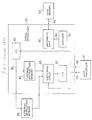
- Fig. 1 is a schematic block diagram of an exemplary conventional signal processor employing the digital signal processor (DSSP1) mainly for voice signal processing published in the preprint No. S10-1 for the Denshi Tsushin Gakkai Tsushin Bumon Zenkoku Taikai Symposium, 1985.
- the digital signal processor is controlled by a host processor.
- a signal processor 82 mainly for signal processing, a host processor 81 for controlling the signal processor 82, an instruction memory selection signal 83, a reset signal 84 for initializing the signal processor 82, a program counter (PC) 85, an instruction address 86, an internal instruction memory 87, such as a ROM, storing instruction words, an external instruction memory 88 storing instruction words, a switching circuit 89 for selecting one of two instruction words according to the instruction memory selection signal 83, an instruction register (IR) 90 for holding an instruction word, a decoder 91 for decoding instruction words, an arithmetic unit 92 which carries out arithmetical operations, a control signal 93, a data memory 94 storing data to be subjected to signal processing operation, and data 95.
- PC program counter
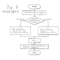
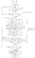
- Fig. 2 is a flow chart of assistance in explaining the operation of the signal processor.
- this signal processor Upon the connection of the signal processor to a power supply, first the host processor starts operation and gives a selection signal 83 to the signal processor 82 to specify the internal instruction memory 87 or the external instruction memory 88. The internal instruction memory 87 is selected when the logical value of the selection signal 83 is "0", while the external instruction memory 88 is selected when the logical value of the selection signal 83 is "1". Then, the host processor 81 gives the reset signal 84 to the signal processor 82. Upon the reception of the reset signal 84, the devices including the internal instruction register are initialized and the PC 85 is cleared.
- the PC 85 gives an instruction address 86 specifying an address 0 to the internal instruction memory 87 of the signal processor 82 and to the external instruction memory 88 to read instruction words stored at the specified address 0 and the instruction words are given to the switching circuit 89.
- the switching circuit 89 selects either the instruction word read from the internal instruction memory 87 or the instruction word read from the external instruction memory 88 according to the selection signal 83 given thereto from the host processor 81 and gives the selected instruction word to the IR 90.
- the instruction word held by the IR 90 is decoded by the decoder 91 to provide control signals to the devices.
- the internal arithmetic unit 92 of the signal processor 82 is controlled by the control signal 93 provided by the decoder 91 to process the data 95 stored in the data memory 94 through arithmetical operations.
- the conventional signal processor needs a comparatively large-scale control program for complex signal processing and the capacity of the internal instruction memory 87 of the signal processor 82 is insufficient to store such a large-scale control program, and hence the external instruction memory 88 is necessary.
- an input/output (I/O) device is necessary for transferring the internal signals of the signal processor 82 and the external signals through external terminals to provide the instruction address 86 and to receive instruction words.
- I/O input/output
- a long time is necessary for reading instruction words from the internal instruction memory 87 because the instruction words are read through an additional device.
- a clock signal having a long period must be applied to the signal processor 82 when the external instruction memory 88 is employed, and the signal processor 82 must be initialized by the reset signal 84 after switching the instruction memories or the signal processor will malfunction.
- the internal instruction memory 87 of the signal processor 82 is a so-called mask ROM in which a program is written beforehand in fabricating the signal processor 82, and a special program for special processes are stored in the internal instruction memory 87.
- the conventional signal processor thus constituted needs to read instruction words from the external instruction memory in executing complex processes requiring additional time for reading instruction words from the external instruction memory to reduce the processing efficiency. Furthermore, since the internal instruction memory is a read-only memory, the change of the program after the completion of the signal processor is impossible and, when errors are found in the program or when the program needs correction, the signal processor needs to be changed for a new one, which deteriorates the efficiency of development and is uneconomical.
- the digital signal processor according to the present invention as claimed incorporates a writable instruction memory as an internal instruction memory, and is controlled by instructions provided by a host processor for temporary stop and restart of operation, and for writing in and reading from the writable instruction memory. Accordingly, the operation of the digital signal processor is stopped temporarily by the host processor, and the operation of the digital signal processor is restarted for other process after the internal instruction memory of the digital signal processor has been rewritten.
- a digital signal processor in a first embodiment, according to the present invention will be described hereinafter.
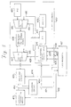
- a host processor 403 a signal processor 404, a hold request signal 405 requesting the temporary stop of instruction execution of the signal processor 404, a hold authorizing signal 406 for informing an external unit of the temporary stop of the signal processor 404, a program counter (PC) 407, an instruction memory control unit 408, a reloadable writable instruction memory 409, an instruction address 410, a switching circuit 411, a selection signal 412, an external instruction memory 413, instruction words 414 and 415, a comparing circuit 416, a result 417 of decision, and write end signal 418.
- the signal processor 404 has an arithmetic unit the same as that of the conventional signal processor, and hence the arithmetic unit is not shown in Fig. 3.
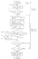
- Fig. 4 is a flow chart of assistance in explaining the operation of the signal processor.
- the host processor 403 gives the signal processor 404 the hold request signal 405 requesting the temporary stop of instruction word execution.
- the signal processor 404 Upon the end of an instruction presently being executed after the reception of the hold request signal 405, the signal processor 404 provides the hold authorizing signal 406 to stop updating the PC 407 and to interrupt the execution of the instruction word temporarily.
- the instruction memory control unit 408 provides the instruction address 410 specifying an address to be reloaded in the writable instruction memory 409, and the selection signal 412 to control the switching circuit 411 so that the instruction address 410 is selected.
- the instruction address 410 is given also to the external instruction memory 413.
- the external instruction memory 413 provides an instruction word 414, which is written in the writable instruction memory 409.
- the instruction word 414 written in the writable instruction memory 409 is read from the writable instruction memory 409.
- the instruction word 415 read from the rewritable instruction memory 409 and the instruction word 414 written in the same are compared by the comparison circuit 416 to decide whether or not the instruction words 414 and 415 coincide with each other.
- the instruction word 414 is not written correctly in the rewritable instruction memory 409, the two instruction words do not coincide with each other.
- a write error flag is set according to the result 417 of decision in the instruction memory control unit 408. This write error signal is not reset until all the write operations are completed.
- the instruction memory control unit 408 of the signal processor 404 Upon the cancellation of the hold request signal 405, the instruction memory control unit 408 of the signal processor 404 provides a selection signal 412 to make the switching circuit 411 select the instruction address of the PC 407, the instruction address of the PC 407 is updated, and then an instruction at an instruction address succeeding the instruction address of the last instruction word executed before the execution of instructions was stopped temporarily is executed.
- the contents of the signal processing process can readily be changed by providing the signal processor with an internal rewritable instruction memory.
- the malfunction of the signal processor attributable to erroneous rewrite can be prevented by providing a verify circuit in the signal processor.
- Fig. 5 shows a signal processor in a second embodiment which is a modification of the signal processor of Fig. 3.
- This modified signal processor is provided externally with a decision circuit for deciding whether or not the contents of the writable instruction memory is correct.
- Fig. 6 is a flow chart of assistance in explaining the operation of the modified signal processor.
- a host processor 421 When the contents of the process to be executed by the signal processor 422 needs to be changed, a host processor 421 provides a hold request signal 405 to stop updating a PC 407 so that the execution of instruction words is interrupted temporarily. Upon the reception of a hold authorizing signal 406, the host processor 421 gives an instruction address 410 to an external instruction memory 413 and the signal processor 422. An instruction word 414 read from the external instruction memory 413 is applied to a switching circuit 423, and then the instruction word 414 is applied to the signal processor 422 when a selection signal 424 is provided by the host processor 421.
- the host processor 421 provides a write control signal 425 to instruct an instruction memory control unit 426 to give a selection signal 428 to the switching circuit 427, so that the instruction word 414 is written in a writable instruction memory 409. Then, the host processor 421 provides a read control signal 429 to read an instruction word 415, i.e., the written instruction word, from the writable instruction memory 409, and the instruction memory control unit 426 gives a selection signal 428 to the switching circuit 427 to apply the instruction word 415 to the switching circuit 423. The host processor 421 provides the selection signal 424 to apply the instruction word 415 to a comparison circuit 430.
- the comparing circuit 430 compares the instruction word 414 read from the external instruction memory 413 and the instruction word 415 read from the writable instruction memory 407, and then gives the result 431 of comparison to the host processor 421.
- the host processor executes operation for writing the next instruction word.
- the host processor performs the same instruction write operation again.
- the host processor 421 cancels the hold request signal 405 to enable the signal processor 422 to restart the operation.
- m x n (m is an integer not less than one and n is an integer not less than two) bit width from the external instruction memory and giving the instruction word to the signal processor
- m x n pieces of external terminals are necessary.
- only m pieces of external terminals are necessary when the bits of the instruction word is divided into bit widths each of m bits and the instruction word is written in the internal writable instruction memory by repeating the write operation n times.
- the signal processor according to the present invention incorporates an internal writable instruction memory, and the operation of the signal processor is stopped temporarily by an instruction provided by the host processor to reload the internal instruction memory of the signal processor, the program stored in the signal processor can optionally be changed after the signal processor has been fabricated, which enhances the efficiency of development activities and is highly economical. Furthermore, the possibility of temporarily stopping the execution of an instruction during the signal processing operation to rewrite the program, and restarting the execution of the instruction after rewriting the program enable the signal processor to perform more complicated signal processing operations and diversifies the signal processing functions of the signal processor for flexible signal processing.
Description
Claims (4)
- A digital signal processing system comprising:characterized by further comprisinga processor (404; 422) mainly for signal processing, having an internal writable instruction memory (409) for storing instruction words (414, 415) specifying various internal operations;means for temporarily stopping and restarting the operation of the processor (404; 422);an instruction memory (413) storing instruction words (414) to be written in the writable instruction memory; anda host processor (403; 421) connected to the processor (404; 412), the stopping and restarting means, and the instruction memory (413) to control the same;means for temporarily stopping the operation of the processor (404; 422) in response to a command (405) provided by the host processor (403; 421), reading an instruction word (414) from the instruction memory (413) and writing the instruction word (414) in the writable instruction memory (409); andmeans (416; 421) for comparing an instruction word (414) read from said instruction memory (413), after the former instruction word (415) read from said instruction memory (413) has been written in said writable instruction memory (409), with the former instruction word (415) read from said writable instruction memory (409), deciding whether or not the former instruction word (415) and the latter instruction word (414) coincide with each other, and for providing the result (417) of decision of the comparison circuit (416), wherein the host processor (403; 421) performs a control operation to write an instruction word again in said writable instruction memory (409) when the former and latter instruction words (415, 414) do not coincide with each other, and wherein the operation of the processor (404; 422) is changed over by restarting the operation of the processor (404; 422) in response to a command (405) provided by the host processor (403; 421) after the instruction word (414) has been written in the writable instruction memory (409);
- The digital signal processing system according to claim 1, whereinan instruction address automatically generated by the processor (404) is applied to said instruction memory (413) in reading an instruction word (414) from said instruction memory (413) and writing the read instruction word (414) in said writable instruction (409); andsaid processor (404) is provided with a comparing circuit (416) as comparing and deciding means and an output means for providing the result (417) of decision of the comparing circuit (416).
- A digital signal processing system according to claim 1, whereinan instruction word (414) is read from said instruction memory (413) according to an instruction address (410) provided by said host processor (421) in reading the instruction word (414) from said instruction memory (413) and writing the instruction word (414) in said writable instruction memory (409), the instruction word (414) written in said writable instruction memory (409) according to an instruction address (410) and a write control signal (425) provided by said host processor (421) is read from said writable instruction memory (40) in response to a read control signal (429) provided by said host processor (421); andsaid host processor (421) compares the instruction word (414) read from said instruction memory (413) and the former instruction word (415) written in said writable instruction memory (409) and decides whether or not these instruction words (414, 415) coincide with each other.
- A digital signal processing system according to anyone of the preceding claims, wherein an instruction word (414) having an m x n bit width (m is an integer not less than one, n is an integer not less than two) is divided in m-bit widths and is read and written in n cycles of read and write operations in reading the instruction word (414) from said instruction memory (413) and writing the instruction word (414) in said writable instruction memory (409).
Applications Claiming Priority (17)
| Application Number | Priority Date | Filing Date | Title |
|---|---|---|---|
| JP140872/87 | 1987-06-05 | ||
| JP14087287A JPS63304344A (en) | 1987-06-05 | 1987-06-05 | Multi-port memory circuit |
| JP18685887A JPS6429932A (en) | 1987-07-27 | 1987-07-27 | Address control system for signal processing |
| JP186858/87 | 1987-07-27 | ||
| JP197009/87 | 1987-08-06 | ||
| JP19700987A JPS6441028A (en) | 1987-08-06 | 1987-08-06 | Interruption processing system |
| JP273763/87 | 1987-10-29 | ||
| JP62273763A JPH0630056B2 (en) | 1987-10-29 | 1987-10-29 | Signal processor |
| JP274810/87 | 1987-10-30 | ||
| JP27481087A JPH01116730A (en) | 1987-10-30 | 1987-10-30 | Digital signal processor |
| JP62296611A JPH0766327B2 (en) | 1987-11-25 | 1987-11-25 | Signal processing method and apparatus |
| JP62296612A JPH0766328B2 (en) | 1987-11-25 | 1987-11-25 | Signal processing method of processor |
| JP296612/87 | 1987-11-25 | ||
| JP296611/87 | 1987-11-25 | ||
| JP316553/87 | 1987-12-15 | ||
| JP31655387A JPH01156825A (en) | 1987-12-15 | 1987-12-15 | Generating system for signal processing address |
| EP88108755A EP0293851B1 (en) | 1987-06-05 | 1988-06-01 | Digital signal processor |
Related Parent Applications (2)
| Application Number | Title | Priority Date | Filing Date |
|---|---|---|---|
| EP88108755A Division EP0293851B1 (en) | 1987-06-05 | 1988-06-01 | Digital signal processor |
| EP88108755.5 Division | 1988-06-01 |
Publications (3)
| Publication Number | Publication Date |
|---|---|
| EP0554917A2 EP0554917A2 (en) | 1993-08-11 |
| EP0554917A3 EP0554917A3 (en) | 1994-04-13 |
| EP0554917B1 true EP0554917B1 (en) | 1998-05-06 |
Family
ID=27573171
Family Applications (6)
| Application Number | Title | Priority Date | Filing Date |
|---|---|---|---|
| EP93104195A Expired - Lifetime EP0551931B1 (en) | 1987-06-05 | 1988-06-01 | Digital signal processor comprising address generator accessing data stored in bidirectional space of data memory |
| EP93104194A Expired - Lifetime EP0554917B1 (en) | 1987-06-05 | 1988-06-01 | Digital signal processing system having two instruction memories accessed by a processor under control of host |
| EP19930104197 Withdrawn EP0551933A3 (en) | 1987-06-05 | 1988-06-01 | Digital signal processor |
| EP88108755A Expired - Lifetime EP0293851B1 (en) | 1987-06-05 | 1988-06-01 | Digital signal processor |
| EP93104196A Expired - Lifetime EP0551932B1 (en) | 1987-06-05 | 1988-06-01 | Digital signal processor processing multi-point conditional branch operations in a pipeline mode |
| EP93104238A Withdrawn EP0551934A2 (en) | 1987-06-05 | 1988-06-01 | Digital signal processor |
Family Applications Before (1)
| Application Number | Title | Priority Date | Filing Date |
|---|---|---|---|
| EP93104195A Expired - Lifetime EP0551931B1 (en) | 1987-06-05 | 1988-06-01 | Digital signal processor comprising address generator accessing data stored in bidirectional space of data memory |
Family Applications After (4)
| Application Number | Title | Priority Date | Filing Date |
|---|---|---|---|
| EP19930104197 Withdrawn EP0551933A3 (en) | 1987-06-05 | 1988-06-01 | Digital signal processor |
| EP88108755A Expired - Lifetime EP0293851B1 (en) | 1987-06-05 | 1988-06-01 | Digital signal processor |
| EP93104196A Expired - Lifetime EP0551932B1 (en) | 1987-06-05 | 1988-06-01 | Digital signal processor processing multi-point conditional branch operations in a pipeline mode |
| EP93104238A Withdrawn EP0551934A2 (en) | 1987-06-05 | 1988-06-01 | Digital signal processor |
Country Status (4)
| Country | Link |
|---|---|
| US (1) | US5045993A (en) |
| EP (6) | EP0551931B1 (en) |
| CA (1) | CA1288169C (en) |
| DE (4) | DE3851858T2 (en) |
Families Citing this family (55)
| Publication number | Priority date | Publication date | Assignee | Title |
|---|---|---|---|---|
| CA1311063C (en) * | 1988-12-16 | 1992-12-01 | Tokumichi Murakami | Digital signal processor |
| JPH0769791B2 (en) * | 1988-12-21 | 1995-07-31 | 三菱電機株式会社 | Microprocessor |
| JPH0740241B2 (en) * | 1989-01-17 | 1995-05-01 | 富士通株式会社 | Request cancellation method |
| US5237670A (en) * | 1989-01-30 | 1993-08-17 | Alantec, Inc. | Method and apparatus for data transfer between source and destination modules |
| US5150471A (en) * | 1989-04-20 | 1992-09-22 | Ncr Corporation | Method and apparatus for offset register address accessing |
| US5175863A (en) * | 1989-10-23 | 1992-12-29 | International Business Machines Corporation | Signal data processing system having independently, simultaneously operable alu and macu |
| EP0843254A3 (en) * | 1990-01-18 | 1999-08-18 | National Semiconductor Corporation | Integrated digital signal processor/general purpose CPU with shared internal memory |
| JPH0444151A (en) * | 1990-06-11 | 1992-02-13 | Omron Corp | Processor |
| JPH0470946A (en) * | 1990-07-04 | 1992-03-05 | Mitsubishi Electric Corp | Processor containing dma controller |
| JP3194193B2 (en) * | 1990-10-31 | 2001-07-30 | カシオ計算機株式会社 | Signal processing device |
| RU1804645C (en) * | 1991-03-27 | 1993-03-23 | Институт Точной Механики И Вычислительной Техники Им.С.А.Лебедева | Central processor |
| FR2678400B1 (en) * | 1991-06-27 | 1995-08-04 | Texas Instruments France | PROTOCOL PROCESSOR FOR EXECUTING A SET OF INSTRUCTIONS IN A REDUCED NUMBER OF OPERATIONS. |
| US7197623B1 (en) | 1991-06-27 | 2007-03-27 | Texas Instruments Incorporated | Multiple processor cellular radio |
| JP3201786B2 (en) * | 1991-07-18 | 2001-08-27 | アジレント・テクノロジー株式会社 | Control method of digital signal processing system |
| JP3172214B2 (en) * | 1991-09-30 | 2001-06-04 | 富士通株式会社 | Status mode setting method |
| JP2906792B2 (en) * | 1991-11-15 | 1999-06-21 | 日本電気株式会社 | Digital processor and control method thereof |
| EP0545581B1 (en) * | 1991-12-06 | 1999-04-21 | National Semiconductor Corporation | Integrated data processing system including CPU core and parallel, independently operating DSP module |
| US6000026A (en) * | 1992-06-22 | 1999-12-07 | Texas Instrument Incorporated | Multiple processor apparatus having a protocol processor intended for the execution of a collection of instructions in a reduced number of operations |
| DE69315630T2 (en) * | 1992-07-23 | 1998-07-16 | Rockwell International Corp | Data access in a RISC digital signal processor |
| US5481489A (en) * | 1992-08-31 | 1996-01-02 | Fujitsu Limited | Method of and apparatus for discriminating NaN |
| US5717908A (en) * | 1993-02-25 | 1998-02-10 | Intel Corporation | Pattern recognition system using a four address arithmetic logic unit |
| US5825921A (en) * | 1993-03-19 | 1998-10-20 | Intel Corporation | Memory transfer apparatus and method useful within a pattern recognition system |
| FR2708359A1 (en) * | 1993-06-30 | 1995-02-03 | Philips Electronics Nv | Method for operating a digital signal processor and device implementing the method |
| DE59408784D1 (en) * | 1993-08-09 | 1999-11-04 | Siemens Ag | Signal processing device |
| JP3452655B2 (en) * | 1993-09-27 | 2003-09-29 | 株式会社日立製作所 | Digital signal processor and method of executing instructions using the same |
| US5778416A (en) * | 1993-12-20 | 1998-07-07 | Motorola, Inc. | Parallel process address generator and method |
| US5590356A (en) * | 1994-08-23 | 1996-12-31 | Massachusetts Institute Of Technology | Mesh parallel computer architecture apparatus and associated methods |
| US5835730A (en) * | 1996-07-31 | 1998-11-10 | General Instrument Corporation Of Delaware | MPEG packet header compression for television modems |
| WO1998006039A1 (en) * | 1996-08-07 | 1998-02-12 | Sun Microsystems, Inc. | Disambiguation memory circuit and operating method |
| WO1998006038A1 (en) * | 1996-08-07 | 1998-02-12 | Sun Microsystems, Inc. | Architectural support for software pipelining of loops |
| WO1998006041A1 (en) * | 1996-08-07 | 1998-02-12 | Sun Microsystems, Inc. | Array prefetch apparatus and method |
| US5958048A (en) * | 1996-08-07 | 1999-09-28 | Elbrus International Ltd. | Architectural support for software pipelining of nested loops |
| WO1998006040A1 (en) * | 1996-08-07 | 1998-02-12 | Sun Microsystems, Inc. | Architectural support for software pipelining of nested loops |
| WO1998006042A1 (en) * | 1996-08-07 | 1998-02-12 | Sun Microsystems, Inc. | Wide instruction unpack method and apparatus |
| US5880981A (en) * | 1996-08-12 | 1999-03-09 | Hitachi America, Ltd. | Method and apparatus for reducing the power consumption in a programmable digital signal processor |
| US6332152B1 (en) * | 1997-12-02 | 2001-12-18 | Matsushita Electric Industrial Co., Ltd. | Arithmetic unit and data processing unit |
| TW380245B (en) * | 1998-05-18 | 2000-01-21 | Winbond Elelctronics Corp | Speech synthesizer and speech synthesis method |
| US7234100B1 (en) * | 2000-09-28 | 2007-06-19 | Intel Corporation | Decoder for trellis-based channel encoding |
| US6662296B1 (en) * | 2000-10-02 | 2003-12-09 | International Business Machines Corporation | Method and system for testing millicode branch points |
| JP2002215606A (en) * | 2001-01-24 | 2002-08-02 | Mitsubishi Electric Corp | Data processor |
| US20020184566A1 (en) | 2001-06-01 | 2002-12-05 | Michael Catherwood | Register pointer trap |
| US20030061464A1 (en) * | 2001-06-01 | 2003-03-27 | Catherwood Michael I. | Digital signal controller instruction set and architecture |
| US7167973B2 (en) * | 2001-11-15 | 2007-01-23 | Broadcom Corporation | Method and system for performing multi-tests in processors using results to set a register and indexing based on the register |
| JP2005149297A (en) * | 2003-11-18 | 2005-06-09 | Renesas Technology Corp | Processor and assembler thereof |
| JP4908017B2 (en) * | 2006-02-28 | 2012-04-04 | 富士通株式会社 | DMA data transfer apparatus and DMA data transfer method |
| US7953958B2 (en) * | 2006-09-29 | 2011-05-31 | Mediatek Inc. | Architecture for joint detection hardware accelerator |
| US20090129486A1 (en) * | 2007-11-15 | 2009-05-21 | Sequel Technologies, Llc. | Systems and methods for providing security communication procesess in a security system |
| GB2500707B (en) * | 2012-03-30 | 2014-09-17 | Cognovo Ltd | Multiprocessor system, apparatus and methods |
| US20150268962A1 (en) * | 2014-03-24 | 2015-09-24 | GoofyFoot Labs | Asynchronous Circuit Design |
| US9817791B2 (en) * | 2015-04-04 | 2017-11-14 | Texas Instruments Incorporated | Low energy accelerator processor architecture with short parallel instruction word |
| US11847427B2 (en) | 2015-04-04 | 2023-12-19 | Texas Instruments Incorporated | Load store circuit with dedicated single or dual bit shift circuit and opcodes for low power accelerator processor |
| US10401412B2 (en) | 2016-12-16 | 2019-09-03 | Texas Instruments Incorporated | Line fault signature analysis |
| US11010953B2 (en) * | 2017-04-21 | 2021-05-18 | Intel Corporation | Dedicated fixed point blending for energy efficiency |
| CN109714056B (en) * | 2019-01-17 | 2022-10-28 | 上海双微导航技术有限公司 | Method for compatible multi-model AD acquisition |
| CN110737618B (en) * | 2019-10-23 | 2021-03-16 | 盛科网络(苏州)有限公司 | Method, device and storage medium for embedded processor to carry out rapid data communication |
Family Cites Families (19)
| Publication number | Priority date | Publication date | Assignee | Title |
|---|---|---|---|---|
| US3570006A (en) * | 1968-01-02 | 1971-03-09 | Honeywell Inc | Multiple branch technique |
| US3875391A (en) * | 1973-11-02 | 1975-04-01 | Raytheon Co | Pipeline signal processor |
| US4025771A (en) * | 1974-03-25 | 1977-05-24 | Hughes Aircraft Company | Pipe line high speed signal processor |
| US4090250A (en) * | 1976-09-30 | 1978-05-16 | Raytheon Company | Digital signal processor |
| DE2710671A1 (en) * | 1977-03-11 | 1978-09-14 | Standard Elektrik Lorenz Ag | CIRCUIT ARRANGEMENT FOR A MICROPROCESSOR TO CONTROL THE DATA STORAGE ACCESS |
| US4240139A (en) * | 1977-09-22 | 1980-12-16 | Tokyo Shibaura Denki Kabushiki Kaisha | Address generating system |
| CA1114518A (en) * | 1977-10-25 | 1981-12-15 | William D. Strecker | Central processor unit for executing instructions with a special operand specifier |
| US4159519A (en) * | 1977-11-21 | 1979-06-26 | Burroughs Corporation | Template family interfacing structure for providing a sequence of microinstructions to a pipelined microprogrammable data processing system |
| US4236206A (en) * | 1978-10-25 | 1980-11-25 | Digital Equipment Corporation | Central processor unit for executing instructions of variable length |
| US4428046A (en) * | 1980-05-05 | 1984-01-24 | Ncr Corporation | Data processing system having a star coupler with contention circuitry |
| US4493019A (en) * | 1980-05-06 | 1985-01-08 | Burroughs Corporation | Pipelined microprogrammed digital data processor employing microinstruction tasking |
| JPS5750052A (en) * | 1980-09-09 | 1982-03-24 | Toshiba Corp | Address extension system |
| US4439839A (en) * | 1981-08-24 | 1984-03-27 | International Telephone And Telegraph Corporation | Dynamically programmable processing element |
| US4654783A (en) * | 1982-07-26 | 1987-03-31 | Data General Corporation | Unique process for loading a microcode control store in a data processing system |
| JPS5979349A (en) * | 1982-10-29 | 1984-05-08 | Toshiba Corp | Arithmetic device |
| US4613935A (en) * | 1983-02-02 | 1986-09-23 | Couleur John F | Method and apparatus for pipe line processing with a single arithmetic logic unit |
| JPS59174948A (en) * | 1983-03-25 | 1984-10-03 | Toshiba Corp | Information processing device |
| US4578750A (en) * | 1983-08-24 | 1986-03-25 | Amdahl Corporation | Code determination using half-adder based operand comparator |
| US4785393A (en) * | 1984-07-09 | 1988-11-15 | Advanced Micro Devices, Inc. | 32-Bit extended function arithmetic-logic unit on a single chip |
-
1988
- 1988-06-01 DE DE3851858T patent/DE3851858T2/en not_active Expired - Fee Related
- 1988-06-01 EP EP93104195A patent/EP0551931B1/en not_active Expired - Lifetime
- 1988-06-01 EP EP93104194A patent/EP0554917B1/en not_active Expired - Lifetime
- 1988-06-01 DE DE3856220T patent/DE3856220T2/en not_active Expired - Fee Related
- 1988-06-01 EP EP19930104197 patent/EP0551933A3/en not_active Withdrawn
- 1988-06-01 EP EP88108755A patent/EP0293851B1/en not_active Expired - Lifetime
- 1988-06-01 DE DE3856175T patent/DE3856175T2/en not_active Expired - Fee Related
- 1988-06-01 EP EP93104196A patent/EP0551932B1/en not_active Expired - Lifetime
- 1988-06-01 DE DE3856219T patent/DE3856219T2/en not_active Expired - Fee Related
- 1988-06-01 EP EP93104238A patent/EP0551934A2/en not_active Withdrawn
- 1988-06-03 CA CA000568527A patent/CA1288169C/en not_active Expired - Fee Related
- 1988-06-03 US US07/201,208 patent/US5045993A/en not_active Expired - Fee Related
Also Published As
| Publication number | Publication date |
|---|---|
| EP0551934A3 (en) | 1994-04-13 |
| DE3856175T2 (en) | 1998-12-17 |
| EP0551934A2 (en) | 1993-07-21 |
| EP0551931B1 (en) | 1998-07-15 |
| EP0551933A3 (en) | 1993-12-15 |
| DE3856219D1 (en) | 1998-08-20 |
| US5045993A (en) | 1991-09-03 |
| DE3851858D1 (en) | 1994-11-24 |
| EP0554917A2 (en) | 1993-08-11 |
| DE3856220T2 (en) | 1999-01-07 |
| EP0551931A2 (en) | 1993-07-21 |
| DE3856219T2 (en) | 1998-11-19 |
| EP0293851B1 (en) | 1994-10-19 |
| CA1288169C (en) | 1991-08-27 |
| EP0551932B1 (en) | 1998-07-15 |
| EP0551931A3 (en) | 1993-12-15 |
| DE3856175D1 (en) | 1998-06-10 |
| EP0293851A3 (en) | 1990-05-09 |
| EP0293851A2 (en) | 1988-12-07 |
| DE3851858T2 (en) | 1995-05-24 |
| EP0551932A2 (en) | 1993-07-21 |
| DE3856220D1 (en) | 1998-08-20 |
| EP0551932A3 (en) | 1993-12-15 |
| EP0551933A2 (en) | 1993-07-21 |
| EP0554917A3 (en) | 1994-04-13 |
Similar Documents
| Publication | Publication Date | Title |
|---|---|---|
| EP0554917B1 (en) | Digital signal processing system having two instruction memories accessed by a processor under control of host | |
| US4831517A (en) | Branch and return on address instruction and methods and apparatus for implementing same in a digital data processing system | |
| JP4868216B2 (en) | Firmware update circuit and firmware update method | |
| US7805562B2 (en) | Microcomputer with configurable communication interfacing | |
| US4274138A (en) | Stored program control system with switching between instruction word systems | |
| KR100541781B1 (en) | Information processing apparatus and method | |
| JPH0799498B2 (en) | Device for correcting erroneous microinstructions | |
| US5701506A (en) | Microcomputer having ROM program which can be altered | |
| US4598402A (en) | System for treatment of single bit error in buffer storage unit | |
| KR100238917B1 (en) | Supervision of microprocessors | |
| JP2875842B2 (en) | Programmable controller | |
| US7096351B2 (en) | Single-chip microcomputer and boot region switching method thereof | |
| US6925522B2 (en) | Device and method capable of changing codes of micro-controller | |
| US5799144A (en) | Microcomputer for resolving problems found in a program stored in a ROM | |
| US20030005212A1 (en) | Method and apparatus for dynamically modifying a stored program | |
| US6535442B2 (en) | Semiconductor memory capable of debugging an incorrect write to or an incorrect erase from the same | |
| JP3055999B2 (en) | Microprogram control device group | |
| JPH0630056B2 (en) | Signal processor | |
| EP1221096A1 (en) | Method and apparatus for modifying microinstructions in a static memory device | |
| JP3182287B2 (en) | Microprocessor | |
| JPH11229953A (en) | Engine controller | |
| JPH04242437A (en) | Control memory error correction device | |
| JPS6125259A (en) | Rewriting control system of memory | |
| JPS6226540A (en) | Data processing circuit | |
| JPS59218555A (en) | Microprogram control device |
Legal Events
| Date | Code | Title | Description |
|---|---|---|---|
| PUAI | Public reference made under article 153(3) epc to a published international application that has entered the european phase |
Free format text: ORIGINAL CODE: 0009012 |
|
| AC | Divisional application: reference to earlier application |
Ref document number: 293851 Country of ref document: EP |
|
| AK | Designated contracting states |
Kind code of ref document: A2 Designated state(s): DE FR GB IT NL SE |
|
| PUAL | Search report despatched |
Free format text: ORIGINAL CODE: 0009013 |
|
| AK | Designated contracting states |
Kind code of ref document: A3 Designated state(s): DE FR GB IT NL SE |
|
| 17P | Request for examination filed |
Effective date: 19940905 |
|
| 17Q | First examination report despatched |
Effective date: 19960826 |
|
| GRAG | Despatch of communication of intention to grant |
Free format text: ORIGINAL CODE: EPIDOS AGRA |
|
| GRAG | Despatch of communication of intention to grant |
Free format text: ORIGINAL CODE: EPIDOS AGRA |
|
| GRAH | Despatch of communication of intention to grant a patent |
Free format text: ORIGINAL CODE: EPIDOS IGRA |
|
| GRAH | Despatch of communication of intention to grant a patent |
Free format text: ORIGINAL CODE: EPIDOS IGRA |
|
| GRAA | (expected) grant |
Free format text: ORIGINAL CODE: 0009210 |
|
| AC | Divisional application: reference to earlier application |
Ref document number: 293851 Country of ref document: EP |
|
| AK | Designated contracting states |
Kind code of ref document: B1 Designated state(s): DE FR GB IT NL SE |
|
| REF | Corresponds to: |
Ref document number: 3856175 Country of ref document: DE Date of ref document: 19980610 |
|
| ET | Fr: translation filed | ||
| ITF | It: translation for a ep patent filed |
Owner name: ING. C. GREGORJ S.P.A. |
|
| PLBE | No opposition filed within time limit |
Free format text: ORIGINAL CODE: 0009261 |
|
| STAA | Information on the status of an ep patent application or granted ep patent |
Free format text: STATUS: NO OPPOSITION FILED WITHIN TIME LIMIT |
|
| 26N | No opposition filed | ||
| EUG | Se: european patent has lapsed | ||
| REG | Reference to a national code |
Ref country code: GB Ref legal event code: IF02 |
|
| REG | Reference to a national code |
Ref country code: GB Ref legal event code: 746 Effective date: 20020306 |
|
| REG | Reference to a national code |
Ref country code: FR Ref legal event code: D6 |
|
| PGFP | Annual fee paid to national office [announced via postgrant information from national office to epo] |
Ref country code: DE Payment date: 20060525 Year of fee payment: 19 |
|
| PGFP | Annual fee paid to national office [announced via postgrant information from national office to epo] |
Ref country code: GB Payment date: 20060531 Year of fee payment: 19 |
|
| PGFP | Annual fee paid to national office [announced via postgrant information from national office to epo] |
Ref country code: SE Payment date: 20060607 Year of fee payment: 19 |
|
| PGFP | Annual fee paid to national office [announced via postgrant information from national office to epo] |
Ref country code: FR Payment date: 20060608 Year of fee payment: 19 |
|
| PGFP | Annual fee paid to national office [announced via postgrant information from national office to epo] |
Ref country code: NL Payment date: 20060615 Year of fee payment: 19 |
|
| PGFP | Annual fee paid to national office [announced via postgrant information from national office to epo] |
Ref country code: IT Payment date: 20060630 Year of fee payment: 19 |
|
| EUG | Se: european patent has lapsed | ||
| GBPC | Gb: european patent ceased through non-payment of renewal fee |
Effective date: 20070601 |
|
| NLV4 | Nl: lapsed or anulled due to non-payment of the annual fee |
Effective date: 20080101 |
|
| REG | Reference to a national code |
Ref country code: FR Ref legal event code: ST Effective date: 20080229 |
|
| PG25 | Lapsed in a contracting state [announced via postgrant information from national office to epo] |
Ref country code: NL Free format text: LAPSE BECAUSE OF NON-PAYMENT OF DUE FEES Effective date: 20080101 Ref country code: DE Free format text: LAPSE BECAUSE OF NON-PAYMENT OF DUE FEES Effective date: 20080101 |
|
| PG25 | Lapsed in a contracting state [announced via postgrant information from national office to epo] |
Ref country code: GB Free format text: LAPSE BECAUSE OF NON-PAYMENT OF DUE FEES Effective date: 20070601 |
|
| PG25 | Lapsed in a contracting state [announced via postgrant information from national office to epo] |
Ref country code: SE Free format text: LAPSE BECAUSE OF NON-PAYMENT OF DUE FEES Effective date: 20070602 |
|
| PG25 | Lapsed in a contracting state [announced via postgrant information from national office to epo] |
Ref country code: FR Free format text: LAPSE BECAUSE OF NON-PAYMENT OF DUE FEES Effective date: 20070702 |
|
| PG25 | Lapsed in a contracting state [announced via postgrant information from national office to epo] |
Ref country code: IT Free format text: LAPSE BECAUSE OF NON-PAYMENT OF DUE FEES Effective date: 20070601 |