EP0554731A2 - Leitungsschnittstelle für Hochgeschwindigkeitsdatenleitung - Google Patents
Leitungsschnittstelle für Hochgeschwindigkeitsdatenleitung Download PDFInfo
- Publication number
- EP0554731A2 EP0554731A2 EP93100997A EP93100997A EP0554731A2 EP 0554731 A2 EP0554731 A2 EP 0554731A2 EP 93100997 A EP93100997 A EP 93100997A EP 93100997 A EP93100997 A EP 93100997A EP 0554731 A2 EP0554731 A2 EP 0554731A2
- Authority
- EP
- European Patent Office
- Prior art keywords
- speed
- line
- internal
- transmission line
- lines
- Prior art date
- Legal status (The legal status is an assumption and is not a legal conclusion. Google has not performed a legal analysis and makes no representation as to the accuracy of the status listed.)
- Granted
Links
Images



Classifications
-
- G—PHYSICS
- G06—COMPUTING OR CALCULATING; COUNTING
- G06F—ELECTRIC DIGITAL DATA PROCESSING
- G06F13/00—Interconnection of, or transfer of information or other signals between, memories, input/output devices or central processing units
- G06F13/38—Information transfer, e.g. on bus
- G06F13/40—Bus structure
- G06F13/4063—Device-to-bus coupling
- G06F13/4068—Electrical coupling
-
- H—ELECTRICITY
- H04—ELECTRIC COMMUNICATION TECHNIQUE
- H04L—TRANSMISSION OF DIGITAL INFORMATION, e.g. TELEGRAPHIC COMMUNICATION
- H04L25/00—Baseband systems
- H04L25/02—Details ; arrangements for supplying electrical power along data transmission lines
- H04L25/14—Channel dividing arrangements, i.e. in which a single bit stream is divided between several baseband channels and reassembled at the receiver
-
- H—ELECTRICITY
- H04—ELECTRIC COMMUNICATION TECHNIQUE
- H04Q—SELECTING
- H04Q11/00—Selecting arrangements for multiplex systems
- H04Q11/04—Selecting arrangements for multiplex systems for time-division multiplexing
-
- Y—GENERAL TAGGING OF NEW TECHNOLOGICAL DEVELOPMENTS; GENERAL TAGGING OF CROSS-SECTIONAL TECHNOLOGIES SPANNING OVER SEVERAL SECTIONS OF THE IPC; TECHNICAL SUBJECTS COVERED BY FORMER USPC CROSS-REFERENCE ART COLLECTIONS [XRACs] AND DIGESTS
- Y02—TECHNOLOGIES OR APPLICATIONS FOR MITIGATION OR ADAPTATION AGAINST CLIMATE CHANGE
- Y02D—CLIMATE CHANGE MITIGATION TECHNOLOGIES IN INFORMATION AND COMMUNICATION TECHNOLOGIES [ICT], I.E. INFORMATION AND COMMUNICATION TECHNOLOGIES AIMING AT THE REDUCTION OF THEIR OWN ENERGY USE
- Y02D10/00—Energy efficient computing, e.g. low power processors, power management or thermal management
Definitions
- the present invention relates to a hight-speed transmission line system and, more particularly, to a line interface for a high-speed transmission line system.
- a high-speed transmission line system with a line interface connected to a high-speed transmission line.
- the line interface is made up of an interface circuit for effecting AMI/TTL or similar conversion, and a line state sensing circuit.
- a signal format on the high-speed transmission line has one period implemented as n time slots TS1-TSn and is maintained even after the high-speed line has been converted to internal lines by the line interface.
- Internal units incorporated in the transmission line system each trnasmits and receives data in one of the time slots TS on the internal lines. Hence, the time slot to be received by each of the internal units is determined on the basis of the location, internal arrangement and so forth of the unit.
- Each internal unit has n blocks for transmitting and receiving data in the time slots on the internal lines.
- the blocks each has a time slot selecting circuit for selecting a time slot, a data transmitting and receiving circuit for transmitting and reeiving data in the time slot selected, and a logic circuit. Further, each block reports the time slot selected by the time slot selecting circuit to the data transmitting and receiving circuit which in turn reports such data to the logic circuit.
- the conventional high-speed transmission line system particularly a system having a plurality of time slot transmitting and receiving blocks in each internal unit, has some problems left unsolved. Namely, n identical time slot selecting circuits are built in each unit, resulting in wasteful circuit arrangement. Since the data transmitting and receiving circuits are connected to the internal lines and built in each internal unit, the individual unit consumes great current to thereby aggravate the current consumption of the entire system.
- an object of the present invention to provide a line interface for a high-speed transmission line system which simplifies internal units and saves current to be consumed by individual internal unit.
- a high-speed transmission line system connected to a high-speed transmission line for transmitting and receiving one time slot of the high-speed transmission line of the present invention comprises m internal units each being made up of n blocks, n low-speed internal lines connected to the m internal units, and a line interface for converting time slots of a signal received over the high-speed transmission line to the n low-speed internal lines and reconstructing the n low-speed internal lines into a single high-speed line and connecting the single high-speed line to the high-speed transmission line.
- the n blocks of each of the m internal units select the same time slots of the n low-speed intenal lines.
- FIG. 1 shows a conventional line interface for a high-speed transmission line system, shown in FIG. 1.
- the system includes a line interface 22 connected to a high-speed transmission line 21.
- the line interface 22 is made up of an interface circuit 23 and a line state sensing circuit 24.
- the interface circuit 23 effects AMI/TTL similar conventional conversion.
- FIG. 2 shows a signal format particular to the high-speed transmission line 21 and having n time slots TS1 to TSn in one period thereof.
- the signal format does not change even after the high-speed line 21 has been converted to an internal line 27 by the line interface 22.
- Units 25-1 to 25-n are incorporated in the system, and each transmits and receives data by using a particular time slot over the internal line. Specifically, a particular time slot is assigned to each of the units 25-1 to 25-n depending on the location, internal arrangement and so forth of the unit.
- the units 25-1 to 25-n (represented by the unit 25-1) has n blocks for transmitting and receiving data over the intenal line 27.
- the n blocks have respectively time slot selecting circuits 32-1 to 32-n, data transmitting and receiving circuits 31-1 to 31-n for transmitting and receiving data in the time slot selected, and logic circuits 33-1 to 33-n. These n blocks are commonly connected to the internal line 27.
- Each of the blocks 1- n reports the time slot selected by associated one of the time slot selecting circuits 32-1 to 32-n to associated one of the data tansmitting and receiving circuits 31-1 to 31-n. Then, the data transmitting and receiving circuit of interest transfers only such data to associated one of the logic circuits 33-1 to 33-n.
- n idetntical time slot selecting circuits 32-1 to 32-n are wastefully built in each of the units 25-1 to 25-n. Moreover, since the data transmitting and receiving circuits connected to the internal line 27 are incorporated in all of the units 25-1 to 25-n, each unit consumes great current. This aggravates the current consumption of the entire system incorporting a great number of such units.
- the system embodying the present invention has a line interface 2 connected to a high-speed transmission line 1.
- the line interface 2 is made up of an interface circuit 3 for, for example, AMI/TTL conversion, a line state sensing circuit 4, a time slot changing circuit 5, a line number changing circuit 6, and a line speed changing circuit 7.
- the line interface 2 is connected to internal units 8-1 to 8-m by internal lines 91- to 9-n.
- the high-speed transmission line 1 is converted to an internal level by the interface circuit 3 and then applied to the time slot changing circuit 5.
- the internal units 8-1 to 8-m each includes m blocks for transmitting and receiving n time slots, i.e., m data transmitting and receiving circuits. Therefore, at least n x m time slots exist on the transmission line 1.
- the time slot changing circuit 5 changes (replaces) the order of time slots depending on which time slot on the transmission line 1 is occupied by which of the internal units 8-1 to 8-m.
- the time slot changing circuit 5 transfers the high-speed line whose time slots have been changed in matching relation to the units 8-1 to 8-m. As shown in FIG.
- the line number changing circuit 6 changes the high-speed line to n lines on a period basis. Specifically, as shwn in FIG. 5, the lines are changed such that the same time slots are assigned to each of n internal lines 9-1 to 9-n, e.g., time slots TS1-1 to TS1-n are assigned to the internal unit 8-1.
- the line speed changing circuit 7 converts the high speed to a low speed and delivers it to the internal lines 9-1 to 9-n. Since the units 8-1 to 8-m are respectively connected to the internal lines 9-1 to 9-n, the time slots to be used by each of the units 8-1 to 8-m are the same on the internal lines. Therefore, it is not necessary to incorporate the same number of time slot selecting circuits as data transmitting and receiving circuits, i.e., a single time slot selecting circuit has only to be built in each of the units 8-1 to 8-m.
- the n internal lines 9-1 to 9-n are inputted to the line speed changing circuit 7 to have their speed changed to the high speed.
- the line number changing circuit 6 converges the lines 9-1 to 9-n to a single line.
- the time slot changing circuit 5 changes the time slots to ones matching the transmission line 1 and delivers the resulting time slots to the interface circuit 3.
- the interface circuit 3 convers the level of the time slots and then feeds them out to the transmission line 1.
- the line interface 2 As shown, the high-speed transmission line 1 and the low-speed internal lines 9 are assumed to have frequencies N1 and N2 (MHz), respectively.
- the line interface 2 accommodates m internal lines 9-1 to 9-M. There are sown in FIG.
- a local phase synchronizing circuit 50 elastic memories 51-1 to 51-M and 52-1 to 52-M, an RR1 generating circuit 53 for generating a read reset signal R1, an RR2 generating circuit 54 for generating a read reset signal RR2, an RR3 generating circuit 55 for generating a read reset signal RR3, a WR1 generating circuit 56 for generating a write reset signal WR1, a WR2 generating circuit 57 for generating a write reset signal WR2, a WR3 generating circuit 58 for generating a write reset signal WR3, a WI1 generating circuit 59 for generating a write inhibit signal WR1, an RI generating circuit 60 for generating signals RI3-1 to RI3-M, a selector 61, and a control signal generating circuit 62.
- a signal from the high-speed transmission line 1 is applied to the local phase synchronizing circuit 50 as data having the frequency N1.
- the local phase synchronization is customary with an ordinary transmission line interface and implemented with a local clock in place of a remote clock which suffers from, for example, jitter.
- the data resulting from the local is stable at the negative-going edges of a basic period signal.
- the beginning of the data output is indicated by the read reset signal RR1.
- the elastic memories 51-1 to 51-M change the time slots, line number, and speed.
- the write reset signals WR initialize the input addresses to the elastic memories 51-1 to 51-M while the write inhibit signal WI generates an input permission timing.
- the output timing is indicated by the read reset signal RR2 and is synchronous with a low-speed line clock CLK (N2 MHz).
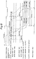
- the low-speed internal lines 9-1 to 9-M are synchronous with the basic synchronizing signal, as shown in FIG. 9.
- the write reset signal WR3 initializes the write addresses of the elastic memories 52-1 to 52-M to thereby write one period of data.
- the data are read out of the elastic memories 52-1 to 52-M in synchronism with the clock (N1) of the high-speed line 1 in response to the read timing generated by the RI generating circuit 60 and meant for each memory. As shown in FIG. 9, this timing differs from one memory to another. As a result, speed and line number are changed.
- a control signal meant for the high-speed line 1 e.g. framing signal
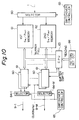
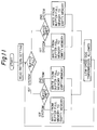
- FIG. 10 shows another specific construction of the interface 2 while FIG. 11 demonstrates a specific operation thereof.
- the construction of FIG. 10 differs from that of FIG. 7 in that it implements the conversion of the time slots with software.
- a first serial IN/parallel OUT memory 61 a second serial IN/parallel OUT memory 62, a CPU (Central Processing Unit) 63, selectors 64-1 to 64-M, a switchover controller 65, and a pattern setting circuit 66.
- data on the high-speed transmission line 1 are serially and alternately applied to the first and second serial IN/parallel OUT memories 61 and 62 every basic period (one frame).
- a signal BUFFER FULL is outputted from the system of interest.
- the CPU 63 reads the data out of the full serial IN/parallel OUT memory 61 or 62 one byte at a time and writes them in a predetermined address (time slot, phase, etc.) of one of the lines 9-1 to 9-M set by the pattern setting circuit 66 and indicating "buffer empty". After data have been written in all the addresses (time slots), the CPU 63 permits transmission and sends the data in synchronism with the low-speed line clock CLK (N2) and at the timing for switching over the selectors 64-1 to 64-M. In the next period, data having been written in the opposite system are sent. At this instant, the low speed to high speed conversion is also effected in the opposite sequence.
- the present invention provides a line interface having a speed changing circuit which replaces a high-speed transmission line with n low speed internal lines.
- data transmitting and receiving circuits in each internal unit operate at low speed, saving power to be consumed by the internal unit.
- time slots which each internal unit uses are the same on all of the internal lines, a single time slot selecting circuit suffices for each internal unit, promoting efficient circuit configuration.
Landscapes
- Engineering & Computer Science (AREA)
- General Engineering & Computer Science (AREA)
- Theoretical Computer Science (AREA)
- Computer Networks & Wireless Communication (AREA)
- Computer Hardware Design (AREA)
- Physics & Mathematics (AREA)
- General Physics & Mathematics (AREA)
- Power Engineering (AREA)
- Signal Processing (AREA)
- Time-Division Multiplex Systems (AREA)
- Communication Control (AREA)
Applications Claiming Priority (3)
| Application Number | Priority Date | Filing Date | Title |
|---|---|---|---|
| JP10501/92 | 1992-01-24 | ||
| JP1050192 | 1992-01-24 | ||
| JP4010501A JP2888004B2 (ja) | 1992-01-24 | 1992-01-24 | 伝送回線インタフェース回路 |
Publications (3)
| Publication Number | Publication Date |
|---|---|
| EP0554731A2 true EP0554731A2 (de) | 1993-08-11 |
| EP0554731A3 EP0554731A3 (en) | 1995-09-06 |
| EP0554731B1 EP0554731B1 (de) | 2000-04-05 |
Family
ID=11751951
Family Applications (1)
| Application Number | Title | Priority Date | Filing Date |
|---|---|---|---|
| EP93100997A Expired - Lifetime EP0554731B1 (de) | 1992-01-24 | 1993-01-22 | Leitungsschnittstelle für Hochgeschwindigkeitsdatenleitung |
Country Status (4)
| Country | Link |
|---|---|
| US (1) | US5369638A (de) |
| EP (1) | EP0554731B1 (de) |
| JP (1) | JP2888004B2 (de) |
| DE (1) | DE69328270T2 (de) |
Families Citing this family (1)
| Publication number | Priority date | Publication date | Assignee | Title |
|---|---|---|---|---|
| US6813251B1 (en) * | 1999-07-27 | 2004-11-02 | Intel Corporation | Split Transaction protocol for a bus system |
Family Cites Families (6)
| Publication number | Priority date | Publication date | Assignee | Title |
|---|---|---|---|---|
| CA1255018A (en) * | 1984-12-27 | 1989-05-30 | Toru Kosugi | System for controlling a change of sequence order of channel data |
| US4597073A (en) * | 1985-08-27 | 1986-06-24 | Data Race, Inc. | Full-duplex split-speed data communication unit for remote DTE |
| US5046067A (en) * | 1988-10-24 | 1991-09-03 | Reliance Comm/Tec Corporation | Digital transmission system |
| DE3785799T2 (de) * | 1986-06-27 | 1993-10-28 | Fujitsu Ltd | Paketdatenübertragungssystem mit Ringtypübertragungsleitung. |
| US4817083A (en) * | 1987-03-06 | 1989-03-28 | American Telephone And Telegraph Company At&T Bell Laboratories | Rearrangeable multiconnection switching networks employing both space division and time division switching |
| JPH0817369B2 (ja) * | 1987-08-17 | 1996-02-21 | 株式会社日立製作所 | 多重集配信装置 |
-
1992
- 1992-01-24 JP JP4010501A patent/JP2888004B2/ja not_active Expired - Fee Related
-
1993
- 1993-01-22 DE DE69328270T patent/DE69328270T2/de not_active Expired - Fee Related
- 1993-01-22 EP EP93100997A patent/EP0554731B1/de not_active Expired - Lifetime
- 1993-01-25 US US08/008,820 patent/US5369638A/en not_active Expired - Lifetime
Also Published As
| Publication number | Publication date |
|---|---|
| EP0554731B1 (de) | 2000-04-05 |
| DE69328270T2 (de) | 2000-08-24 |
| EP0554731A3 (en) | 1995-09-06 |
| US5369638A (en) | 1994-11-29 |
| DE69328270D1 (de) | 2000-05-11 |
| JP2888004B2 (ja) | 1999-05-10 |
| JPH05268290A (ja) | 1993-10-15 |
Similar Documents
| Publication | Publication Date | Title |
|---|---|---|
| US5323426A (en) | Elasticity buffer for data/clock synchronization | |
| CA2114930C (en) | Method and apparatus for dynamic bandwidth allocation in a digital communication session | |
| US6163545A (en) | System and method for data transfer across multiple clock domains | |
| US4979166A (en) | Multiplexing apparatus | |
| EP0910014B1 (de) | Verfahren und Vorrichtung zum Programmladen | |
| EP1239594B1 (de) | Methode und System für wirksamen Datenaustausch | |
| US5572676A (en) | Network I/O device having fifo for synchronous and asynchronous operation | |
| EP0554731B1 (de) | Leitungsschnittstelle für Hochgeschwindigkeitsdatenleitung | |
| US6546451B1 (en) | Method and apparatus for decoupling processor speed from memory subsystem speed in a node controller | |
| US4004275A (en) | Self-clocking data entry unit system | |
| JP2001344187A (ja) | ホストインタフェース回路 | |
| US6505304B1 (en) | Timer apparatus which can simultaneously control a plurality of timers | |
| JPH0482082A (ja) | 半導体記憶装置 | |
| KR100361511B1 (ko) | 다기능 직렬 통신 인터페이스 장치 | |
| JPH0618373B2 (ja) | データ伝送方法及び装置 | |
| JP3411109B2 (ja) | フレーム位相同期回路 | |
| JP2766006B2 (ja) | エラスティック・ストア方式 | |
| JPS6123707B2 (de) | ||
| KR100313933B1 (ko) | 데이터전송제어장치 | |
| KR100353816B1 (ko) | 통신용 수신 장치 | |
| KR100263670B1 (ko) | 직접 기억 장소 접근 컨트롤러 | |
| JP2004185175A (ja) | 拡張用fifo回路及び送受信装置 | |
| JPS60117286A (ja) | 映像表示制御装置 | |
| JPH05252148A (ja) | クロック乗換回路 | |
| JPH1132383A (ja) | 時分割スイッチ |
Legal Events
| Date | Code | Title | Description |
|---|---|---|---|
| PUAI | Public reference made under article 153(3) epc to a published international application that has entered the european phase |
Free format text: ORIGINAL CODE: 0009012 |
|
| AK | Designated contracting states |
Kind code of ref document: A2 Designated state(s): DE FR GB NL |
|
| PUAL | Search report despatched |
Free format text: ORIGINAL CODE: 0009013 |
|
| AK | Designated contracting states |
Kind code of ref document: A3 Designated state(s): DE FR GB NL |
|
| 17P | Request for examination filed |
Effective date: 19950725 |
|
| 16A | New documents despatched to applicant after publication of the search report | ||
| 17Q | First examination report despatched |
Effective date: 19980522 |
|
| GRAG | Despatch of communication of intention to grant |
Free format text: ORIGINAL CODE: EPIDOS AGRA |
|
| GRAG | Despatch of communication of intention to grant |
Free format text: ORIGINAL CODE: EPIDOS AGRA |
|
| GRAH | Despatch of communication of intention to grant a patent |
Free format text: ORIGINAL CODE: EPIDOS IGRA |
|
| GRAH | Despatch of communication of intention to grant a patent |
Free format text: ORIGINAL CODE: EPIDOS IGRA |
|
| GRAA | (expected) grant |
Free format text: ORIGINAL CODE: 0009210 |
|
| AK | Designated contracting states |
Kind code of ref document: B1 Designated state(s): DE FR GB NL |
|
| PG25 | Lapsed in a contracting state [announced via postgrant information from national office to epo] |
Ref country code: NL Free format text: LAPSE BECAUSE OF FAILURE TO SUBMIT A TRANSLATION OF THE DESCRIPTION OR TO PAY THE FEE WITHIN THE PRESCRIBED TIME-LIMIT Effective date: 20000405 |
|
| REF | Corresponds to: |
Ref document number: 69328270 Country of ref document: DE Date of ref document: 20000511 |
|
| ET | Fr: translation filed | ||
| NLV1 | Nl: lapsed or annulled due to failure to fulfill the requirements of art. 29p and 29m of the patents act | ||
| PLBE | No opposition filed within time limit |
Free format text: ORIGINAL CODE: 0009261 |
|
| STAA | Information on the status of an ep patent application or granted ep patent |
Free format text: STATUS: NO OPPOSITION FILED WITHIN TIME LIMIT |
|
| 26N | No opposition filed | ||
| REG | Reference to a national code |
Ref country code: GB Ref legal event code: IF02 |
|
| PGFP | Annual fee paid to national office [announced via postgrant information from national office to epo] |
Ref country code: FR Payment date: 20060110 Year of fee payment: 14 |
|
| PGFP | Annual fee paid to national office [announced via postgrant information from national office to epo] |
Ref country code: GB Payment date: 20060118 Year of fee payment: 14 |
|
| PGFP | Annual fee paid to national office [announced via postgrant information from national office to epo] |
Ref country code: DE Payment date: 20060119 Year of fee payment: 14 |
|
| PG25 | Lapsed in a contracting state [announced via postgrant information from national office to epo] |
Ref country code: DE Free format text: LAPSE BECAUSE OF NON-PAYMENT OF DUE FEES Effective date: 20070801 |
|
| GBPC | Gb: european patent ceased through non-payment of renewal fee |
Effective date: 20070122 |
|
| REG | Reference to a national code |
Ref country code: FR Ref legal event code: ST Effective date: 20070930 |
|
| PG25 | Lapsed in a contracting state [announced via postgrant information from national office to epo] |
Ref country code: GB Free format text: LAPSE BECAUSE OF NON-PAYMENT OF DUE FEES Effective date: 20070122 |
|
| PG25 | Lapsed in a contracting state [announced via postgrant information from national office to epo] |
Ref country code: FR Free format text: LAPSE BECAUSE OF NON-PAYMENT OF DUE FEES Effective date: 20070131 |