EP0551529A1 - Ersetzungsverfahren für Chips - Google Patents
Ersetzungsverfahren für Chips Download PDFInfo
- Publication number
- EP0551529A1 EP0551529A1 EP91121799A EP91121799A EP0551529A1 EP 0551529 A1 EP0551529 A1 EP 0551529A1 EP 91121799 A EP91121799 A EP 91121799A EP 91121799 A EP91121799 A EP 91121799A EP 0551529 A1 EP0551529 A1 EP 0551529A1
- Authority
- EP
- European Patent Office
- Prior art keywords
- board
- wiring
- card module
- fan
- contact means
- Prior art date
- Legal status (The legal status is an assumption and is not a legal conclusion. Google has not performed a legal analysis and makes no representation as to the accuracy of the status listed.)
- Granted
Links
Images


Classifications
-
- H—ELECTRICITY
- H05—ELECTRIC TECHNIQUES NOT OTHERWISE PROVIDED FOR
- H05K—PRINTED CIRCUITS; CASINGS OR CONSTRUCTIONAL DETAILS OF ELECTRIC APPARATUS; MANUFACTURE OF ASSEMBLAGES OF ELECTRICAL COMPONENTS
- H05K3/00—Apparatus or processes for manufacturing printed circuits
- H05K3/22—Secondary treatment of printed circuits
- H05K3/225—Correcting or repairing of printed circuits
-
- H—ELECTRICITY
- H01—ELECTRIC ELEMENTS
- H01L—SEMICONDUCTOR DEVICES NOT COVERED BY CLASS H10
- H01L24/00—Arrangements for connecting or disconnecting semiconductor or solid-state bodies; Methods or apparatus related thereto
- H01L24/98—Methods for disconnecting semiconductor or solid-state bodies
-
- H—ELECTRICITY
- H05—ELECTRIC TECHNIQUES NOT OTHERWISE PROVIDED FOR
- H05K—PRINTED CIRCUITS; CASINGS OR CONSTRUCTIONAL DETAILS OF ELECTRIC APPARATUS; MANUFACTURE OF ASSEMBLAGES OF ELECTRICAL COMPONENTS
- H05K13/00—Apparatus or processes specially adapted for manufacturing or adjusting assemblages of electric components
- H05K13/04—Mounting of components, e.g. of leadless components
- H05K13/0486—Replacement and removal of components
-
- H—ELECTRICITY
- H05—ELECTRIC TECHNIQUES NOT OTHERWISE PROVIDED FOR
- H05K—PRINTED CIRCUITS; CASINGS OR CONSTRUCTIONAL DETAILS OF ELECTRIC APPARATUS; MANUFACTURE OF ASSEMBLAGES OF ELECTRICAL COMPONENTS
- H05K1/00—Printed circuits
- H05K1/02—Details
- H05K1/14—Structural association of two or more printed circuits
- H05K1/141—One or more single auxiliary printed circuits mounted on a main printed circuit, e.g. modules, adapters
-
- H—ELECTRICITY
- H05—ELECTRIC TECHNIQUES NOT OTHERWISE PROVIDED FOR
- H05K—PRINTED CIRCUITS; CASINGS OR CONSTRUCTIONAL DETAILS OF ELECTRIC APPARATUS; MANUFACTURE OF ASSEMBLAGES OF ELECTRICAL COMPONENTS
- H05K2201/00—Indexing scheme relating to printed circuits covered by H05K1/00
- H05K2201/04—Assemblies of printed circuits
- H05K2201/049—PCB for one component, e.g. for mounting onto mother PCB
-
- H—ELECTRICITY
- H05—ELECTRIC TECHNIQUES NOT OTHERWISE PROVIDED FOR
- H05K—PRINTED CIRCUITS; CASINGS OR CONSTRUCTIONAL DETAILS OF ELECTRIC APPARATUS; MANUFACTURE OF ASSEMBLAGES OF ELECTRICAL COMPONENTS
- H05K2201/00—Indexing scheme relating to printed circuits covered by H05K1/00
- H05K2201/09—Shape and layout
- H05K2201/09009—Substrate related
- H05K2201/09036—Recesses or grooves in insulating substrate
-
- H—ELECTRICITY
- H05—ELECTRIC TECHNIQUES NOT OTHERWISE PROVIDED FOR
- H05K—PRINTED CIRCUITS; CASINGS OR CONSTRUCTIONAL DETAILS OF ELECTRIC APPARATUS; MANUFACTURE OF ASSEMBLAGES OF ELECTRICAL COMPONENTS
- H05K2201/00—Indexing scheme relating to printed circuits covered by H05K1/00
- H05K2201/10—Details of components or other objects attached to or integrated in a printed circuit board
- H05K2201/10613—Details of electrical connections of non-printed components, e.g. special leads
- H05K2201/10621—Components characterised by their electrical contacts
- H05K2201/10681—Tape Carrier Package [TCP]; Flexible sheet connector
-
- H—ELECTRICITY
- H05—ELECTRIC TECHNIQUES NOT OTHERWISE PROVIDED FOR
- H05K—PRINTED CIRCUITS; CASINGS OR CONSTRUCTIONAL DETAILS OF ELECTRIC APPARATUS; MANUFACTURE OF ASSEMBLAGES OF ELECTRICAL COMPONENTS
- H05K2203/00—Indexing scheme relating to apparatus or processes for manufacturing printed circuits covered by H05K3/00
- H05K2203/02—Details related to mechanical or acoustic processing, e.g. drilling, punching, cutting, using ultrasound
- H05K2203/0228—Cutting, sawing, milling or shearing
-
- H—ELECTRICITY
- H05—ELECTRIC TECHNIQUES NOT OTHERWISE PROVIDED FOR
- H05K—PRINTED CIRCUITS; CASINGS OR CONSTRUCTIONAL DETAILS OF ELECTRIC APPARATUS; MANUFACTURE OF ASSEMBLAGES OF ELECTRICAL COMPONENTS
- H05K2203/00—Indexing scheme relating to apparatus or processes for manufacturing printed circuits covered by H05K3/00
- H05K2203/04—Soldering or other types of metallurgic bonding
- H05K2203/049—Wire bonding
-
- H—ELECTRICITY
- H05—ELECTRIC TECHNIQUES NOT OTHERWISE PROVIDED FOR
- H05K—PRINTED CIRCUITS; CASINGS OR CONSTRUCTIONAL DETAILS OF ELECTRIC APPARATUS; MANUFACTURE OF ASSEMBLAGES OF ELECTRICAL COMPONENTS
- H05K2203/00—Indexing scheme relating to apparatus or processes for manufacturing printed circuits covered by H05K3/00
- H05K2203/17—Post-manufacturing processes
- H05K2203/176—Removing, replacing or disconnecting component; Easily removable component
-
- H—ELECTRICITY
- H05—ELECTRIC TECHNIQUES NOT OTHERWISE PROVIDED FOR
- H05K—PRINTED CIRCUITS; CASINGS OR CONSTRUCTIONAL DETAILS OF ELECTRIC APPARATUS; MANUFACTURE OF ASSEMBLAGES OF ELECTRICAL COMPONENTS
- H05K3/00—Apparatus or processes for manufacturing printed circuits
- H05K3/0011—Working of insulating substrates or insulating layers
- H05K3/0044—Mechanical working of the substrate, e.g. drilling or punching
-
- Y—GENERAL TAGGING OF NEW TECHNOLOGICAL DEVELOPMENTS; GENERAL TAGGING OF CROSS-SECTIONAL TECHNOLOGIES SPANNING OVER SEVERAL SECTIONS OF THE IPC; TECHNICAL SUBJECTS COVERED BY FORMER USPC CROSS-REFERENCE ART COLLECTIONS [XRACs] AND DIGESTS
- Y10—TECHNICAL SUBJECTS COVERED BY FORMER USPC
- Y10T—TECHNICAL SUBJECTS COVERED BY FORMER US CLASSIFICATION
- Y10T29/00—Metal working
- Y10T29/49—Method of mechanical manufacture
- Y10T29/49002—Electrical device making
- Y10T29/49117—Conductor or circuit manufacturing
- Y10T29/49124—On flat or curved insulated base, e.g., printed circuit, etc.
- Y10T29/49126—Assembling bases
Definitions
- the invention refers to a method for replacing chips directly attached on boards (also called chip-on-board packaging). Further described is an adapted board and replacement module which both can be used to perform the method and the resulting board.
- the best packaging for the future may be as few levels of packaging as possible for a given application. This might be realized directly mounting the chip on the board.
- This so-called direct chip attach (DCA) or chip-on-board (COB) packaging can provide the smallest and cheapest package among various packaging technologies.
- the devices directly attached on the boards are usually electrically connected by wire bond or tape automated bonding (TAB) technology which will further need protection from process chemicals, dust and humidity.
- TAB tape automated bonding
- IBM Technical Disclosure Bulletin, Vol. 31, No. 3, August 1988, p. 39 shows the test and repair of direct chip attach modules which are C4-bonded (controlled collapsed chip connection), in which a thermode is placed on the back side of the substrate on which the chip is directly attached. The thermode is used to reflow the solder and allowing the chip removal. This method only can be used with single layer substrates and nonsealed chips.
- the present invention as claimed therefore is intended to remedy these drawbacks by providing a new replacement technique for directly attached chips.
- the electronic component which usually is a chip with a plurality of input and output (I/O) terminals arranged close together, needs a fan-out wiring which matches the distances usually used between the wiring lines on the board to the small distances between the I/O terminals of the chip.
- the fan-out wiring area is the region around the chip in which the chip I/O terminal distances are matched to board wiring distances. In this area at least the wiring and the chip are removed to provide a usually rectangular region on the board without wiring and chip.
- the removal at least a thin layer of the board will also be removed; but it is also possible to provide a recess in the board. In a multilayer printed circuit board this recess should have a depth which does not influence the next wiring layer.
- the mechanical removal can be accomplished by appropriate methods well known to a person skilled in the art which are exact enough to provide a defined region with a defined depth.
- a preferred mechanical removal technique is micro milling.
- a card module is placed and fixed on the board at the location of said removed electronic component and said fan-out wiring area such that the card module wiring matches with the board wiring.
- the card module which has the same wiring layout like the wiring on the board before removal and on which a chip is also directly attached, is placed in the wiring free region on the board.
- the card module has the same size like the wiring free region so that the card module can be inserted in the recess to provide as short connections as possible between the card module and the wiring on the board. It is also possible to use a card module having contact means on the bottom side and which are a little amount larger than the free region in order to contact the wiring on the board by solder balls.
- the fixing of the card module is accomplished by common bonding agents.
- the wiring of said board is electrically connected with the wiring of said card module. This can be accomplished by wire bonding or tape automated bonding or other appropriate solder techniques.
- an adapted printed circuit board is used with at least one wiring layer on top of the board which comprises connection lines connecting the contact pads of different electronic components and at least one electronic component directly attached to the board.
- the board can be a multilayer board or a board only having wiring on the top and/or bottom surface.
- the board comprises contact means which are arranged on the wiring lines leading to the contact pads of said directly attached component in a predetermined distance to said component.
- the contact means serve for the electrical connection of the wiring lines on the board to the wiring lines on the card module.
- the electrical connection can be performed by wire bonding, tape automated bonding or other appropriate solder bonding.
- the contact means may comprise lands or blind holes or what ever is appropriate dependent from the preferred connecting principle.
- Solder bonding might be used by providing an adapted card module with soldered contact means at the side of the chip carrying carrier which is inserted in a recess so that the blind hole electrically contacts the contact means on the card module. It is an important feature that these contact means are arranged on the wiring of the board adjacent the fan-out wiring area to allow a replacement of a directly attached chip and its corresponding fan-out wiring area by a card module with the same chip and fan-out wiring. On the other hand the contact means should be as close as possible to the fan-out wiring area in order to have short connecting wires to the card module and to have a small free region. In a very simple embodiment the board the design of the board comprises around the places where chips are directly attached lands on the wiring such that the chip and the respective fan-out wiring can be removed and completely disconnected.
- a card module which comprises a thin carrier card with an electronic component directly attached thereto and connected to a fan-out wiring which ends at the edges of said carrier and contact means for electrically connecting said wiring to the wiring of said board.
- the carrier can be made of the usual card material (organic or anorganic material) and the thickness as low as possible to provide a card module which can be handled and which requires a short connection wiring to the board.
- the chip on the card is also directly attached and connected as usual to a fan-out wiring on the carrier card. The arrangement of the chip and the fan-out correspond with the respective fan-out and chip on the printed circuit board.
- the fan-out wiring should terminate at the edges of the carrier card for allowing short connections to the board.
- the contact means on the card module are preferably arranged at the end of the fan-out wiring and comprise lands on the top or vias on the bottom side of the card module, latter for providing an electrical contact to the board wiring via solder balls.
- contact areas preferably covered with solder may extend over the sides of the card module for electrically contact respective areas in a recess on the board.
- the chip on the card module can be covered by an encapsulant.
- the card module is functionally identical to the direct chip attach site on the board with additional contact means for electrical connections.
- the size of the card module depends mainly on the size of the chip, the number of connections and the geometry of used groundrules.
- the invention refers to a printed circuit board with at least one wiring layer on top of the board which comprises connection lines for connecting the different electronic components.
- the board comprises contact means in a predetermined distance to said component and adjacent to the fan-out wiring area which are arranged on the wiring lines leading to the contact pads of at least one of the components.
- the board comprises a thin card module carrying directly attached one component and the corresponding fan-out wiring area and card contact means.
- the card module is directly fixed to the board such, that the fan-out matches with the wiring on the board.
- Connecting means connect the board contact means with the card contact means.
- This board can be the result after replacing a previous damaged chip by a new replacement chip or a general concept for fixing sensitive chips on a board.
- the card module can be arranged in a recess and the contact means on the board are contact lands which are wire bonded with the contact means on the carrier of the card module.
- the card module can also be fixed and electrically connected as already discussed above by solder balls or TAB technology.
- the present invention has the advantage to provide a complete solution to the direct chip attach replacement problem which allows cost saving because the board having one defect directly attached chip will not be scrap anymore but can easily be reworked.
- This can be prepared by a simple change of the layout of the board.
- the card module can be prepared and tested inclusive burn-in stress test prior usage (which is not possible on the original DCA chip). The removal can be accomplished by well known and exact mechanical methods.
- the wiring 2 on the board 4 (from which only a part is depicted) is provided with lands 6 in a predetermined distance to the chip 8.
- the lands 6 are arranged adjacent the fan-out wiring area 10 in which the small distances of the chip pads 12 are adapted to the wider distances necessary for the board wiring.
- the board will be a multilayer printed circuit board.
- the chip can be connected by C4 technology with the face down to the board or by TAB or wire bond technology. As mentioned above also other suitable bonding technics can be used. For the purpose of clarity the encapsulant usually protecting the chip is not shown.
- Fig. 2 shows the top view of a part of the wiring design on the top of the printed circuit board 4.
- the chip is connected to the board by a controlled collapsed chip connection (C4).
- C4 controlled collapsed chip connection
- a part of the chip 8 is broken away.
- lands 6 on the wiring 2 are indicated.
- a cutting line 14 is shown between the fan-out wiring area 10 and the lands 6 .
- the design of the fan-out wiring and the lands must assure that a complete disconnection of the fan-out wiring of chip which shall be replaced is accomplished.
- the geometry of the lands 6 has to correspond to the appropriate design specifications, e.g. 400 ⁇ m wiring, land size 200 ⁇ m x 300 ⁇ m, 200 ⁇ m spacing.
- a defect directly attached chip and the fan-out wiring area 10 are removed by micro milling thereby providing a recess 16 in the board 4.
- the recess has the size of the fan-out wiring area 10.
- the border 18 of the recess 16 corresponds with the cutting line 14 of Fig. 2.
- the depth of the recess 16 is such that the wiring in the board leading to the removed chip is effectively broken but the wiring planes located in a multilayer board below the recess remain unchanged.
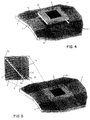
- Fig. 4 shows the board 4 with the wiring 2 and the recess 16 in which a card module 20 is inserted.
- the card module 20 comprises a fully tested chip 9 which is connected to a fan-out wiring 11 arranged on the carrier 22.
- the carrier 22 has the size of the recess 16 and a thickness of 0.3 to 0.7 mm which corresponds to the depth of the recess.
- the fan-out wiring comprises at the edges of carrier 22 also lands 24 which are used to electrically connect the fan-out wiring of the card module to the wiring of the board.
- the fan-out wiring is adapted to the board wiring an corresponds with the removed fan-out wiring.
- a complete board 4 which comprises the card module 20 as depicted in Fig. 4 inserted and fixed, e.g. by glueing with an adhesive, in the recess 16.
- the fan-out wiring 10 of the card module 20 is connected via wire bonds 26 to the wiring 2 on the board 4 as shown in an enlarged detail view.
- the gap 26 between the card module 20 and the board 4 should be as small as possible to provide short wire bonds 26.
- the wire bonds 26 are also protected by a resin encapsulant (for purpose of clarity not shown).
- On the complete board with the fixed and placed card module inserted in the recess it is not recognizable whether a defect chip and fan-out have been at the same location before. Thus, in under special circumstances a board might be constructed in this way with fully tested card modules.
Landscapes
- Engineering & Computer Science (AREA)
- Microelectronics & Electronic Packaging (AREA)
- Manufacturing & Machinery (AREA)
- Computer Hardware Design (AREA)
- Power Engineering (AREA)
- Structures For Mounting Electric Components On Printed Circuit Boards (AREA)
- Credit Cards Or The Like (AREA)
- Electric Connection Of Electric Components To Printed Circuits (AREA)
Priority Applications (3)
| Application Number | Priority Date | Filing Date | Title |
|---|---|---|---|
| EP91121799A EP0551529B1 (de) | 1991-12-19 | 1991-12-19 | Ersetzungsverfahren für Chips |
| DE69120282T DE69120282T2 (de) | 1991-12-19 | 1991-12-19 | Ersetzungsverfahren für Chips |
| US07/986,826 US5519579A (en) | 1991-12-19 | 1992-12-08 | Method and apparatus for replacing directly attached chip |
Applications Claiming Priority (1)
| Application Number | Priority Date | Filing Date | Title |
|---|---|---|---|
| EP91121799A EP0551529B1 (de) | 1991-12-19 | 1991-12-19 | Ersetzungsverfahren für Chips |
Publications (2)
| Publication Number | Publication Date |
|---|---|
| EP0551529A1 true EP0551529A1 (de) | 1993-07-21 |
| EP0551529B1 EP0551529B1 (de) | 1996-06-12 |
Family
ID=8207450
Family Applications (1)
| Application Number | Title | Priority Date | Filing Date |
|---|---|---|---|
| EP91121799A Expired - Lifetime EP0551529B1 (de) | 1991-12-19 | 1991-12-19 | Ersetzungsverfahren für Chips |
Country Status (3)
| Country | Link |
|---|---|
| US (1) | US5519579A (de) |
| EP (1) | EP0551529B1 (de) |
| DE (1) | DE69120282T2 (de) |
Families Citing this family (2)
| Publication number | Priority date | Publication date | Assignee | Title |
|---|---|---|---|---|
| JP6064584B2 (ja) * | 2012-12-22 | 2017-01-25 | 日亜化学工業株式会社 | 発光装置及びその製造方法 |
| JP2021141251A (ja) * | 2020-03-06 | 2021-09-16 | キオクシア株式会社 | 電子部品の切削方法、部品の除去方法及び電子機器の製造方法 |
Citations (1)
| Publication number | Priority date | Publication date | Assignee | Title |
|---|---|---|---|---|
| EP0083265A1 (de) * | 1981-12-22 | 1983-07-06 | Socapex | Verbindungsträger eines integrierten Schaltungsgehäuses auf einer gedruckten Schaltung, und Verbindungssystem mit solchem Träger |
Family Cites Families (8)
| Publication number | Priority date | Publication date | Assignee | Title |
|---|---|---|---|---|
| US4705917A (en) * | 1985-08-27 | 1987-11-10 | Hughes Aircraft Company | Microelectronic package |
| US4907128A (en) * | 1988-12-15 | 1990-03-06 | Grumman Aerospace Corporation | Chip to multilevel circuit board bonding |
| JPH02292836A (ja) * | 1989-05-02 | 1990-12-04 | Nippon Steel Corp | Icチップ実装用フィルムキャリア |
| US5013687A (en) * | 1989-07-27 | 1991-05-07 | Grumman Aerospace Corporation | Framed chip hybrid stacked layer assembly |
| US5231304A (en) * | 1989-07-27 | 1993-07-27 | Grumman Aerospace Corporation | Framed chip hybrid stacked layer assembly |
| JPH0727927B2 (ja) * | 1990-03-12 | 1995-03-29 | 株式会社東芝 | テープキャリア |
| JP2744685B2 (ja) * | 1990-08-08 | 1998-04-28 | 三菱電機株式会社 | 半導体装置 |
| US5093708A (en) * | 1990-08-20 | 1992-03-03 | Grumman Aerospace Corporation | Multilayer integrated circuit module |
-
1991
- 1991-12-19 DE DE69120282T patent/DE69120282T2/de not_active Expired - Fee Related
- 1991-12-19 EP EP91121799A patent/EP0551529B1/de not_active Expired - Lifetime
-
1992
- 1992-12-08 US US07/986,826 patent/US5519579A/en not_active Expired - Lifetime
Patent Citations (1)
| Publication number | Priority date | Publication date | Assignee | Title |
|---|---|---|---|---|
| EP0083265A1 (de) * | 1981-12-22 | 1983-07-06 | Socapex | Verbindungsträger eines integrierten Schaltungsgehäuses auf einer gedruckten Schaltung, und Verbindungssystem mit solchem Träger |
Non-Patent Citations (1)
| Title |
|---|
| IBM TECHNICAL DISCLOSURE BULLETIN vol. 31, no. 11, April 1989, page 214; 'CHIP REMOVAL METHOD' * |
Also Published As
| Publication number | Publication date |
|---|---|
| US5519579A (en) | 1996-05-21 |
| EP0551529B1 (de) | 1996-06-12 |
| DE69120282D1 (de) | 1996-07-18 |
| DE69120282T2 (de) | 1996-12-05 |
Similar Documents
| Publication | Publication Date | Title |
|---|---|---|
| US5280193A (en) | Repairable semiconductor multi-package module having individualized package bodies on a PC board substrate | |
| US7666035B2 (en) | Back-to-back PCB USB connector | |
| US6144090A (en) | Ball grid array package having electrodes on peripheral side surfaces of a package board | |
| KR0157284B1 (ko) | 솔더 볼 장착홈을 갖는 인쇄 회로 기판과 이를 사용한 볼 그리드 어레이 패키지 | |
| EP0653789A2 (de) | Elektronische Gehäusungsstruktur und ihre Herstellung | |
| US6469377B1 (en) | Semiconductor device | |
| KR101177925B1 (ko) | 와이어 본딩된 낮은 프로파일의 usb 디바이스 | |
| US5881453A (en) | Method for mounting surface mount devices to a circuit board | |
| US5184284A (en) | Method and apparatus for implementing engineering changes for integrated circuit module | |
| EP0685990B1 (de) | Einrichtung zum Montieren von elektrischen Teilen auf einer Leiterplatte | |
| EP0551529B1 (de) | Ersetzungsverfahren für Chips | |
| US20110247210A1 (en) | Process for the wafer-scale fabrication of electronic modules for surface mounting | |
| KR100196119B1 (ko) | 반도체장치 및 그 제조방법 및 전자 장치 | |
| CN210042351U (zh) | 一种pcb单板和pcb拼版 | |
| EP0171783A2 (de) | Modulträger und Modul, der diesen Träger benutzt und Verfahren zur Behandlung derselben | |
| JP3009783B2 (ja) | プリント配線基板の製造方法 | |
| EP0413542A2 (de) | Halbleiterpackung für direkte Montierung | |
| KR20070030518A (ko) | 수동 소자 보호용 완충 수단을 구비하는 메모리 모듈 | |
| US5400219A (en) | Tape automated bonding for electrically connecting semiconductor chips to substrates | |
| JPH05275838A (ja) | 電子装置用モジュール | |
| KR20010004340A (ko) | 반도체패키지용 인쇄회로기판 스트립의 구조 및 불량 유닛이 제거된 양호한 인쇄회로기판 스트립의 제조방법 | |
| JPH08340164A (ja) | Bga型パッケージの面実装構造 | |
| KR20070002893A (ko) | 전기과부하 피해 방지용 와이어본딩 장치 | |
| KR100362502B1 (ko) | 가요성회로기판스트립을이용하여제조되는볼그리드어레이반도체패키지의싱글레이션방법및장치 | |
| JP3538179B2 (ja) | 半導体装置 |
Legal Events
| Date | Code | Title | Description |
|---|---|---|---|
| PUAI | Public reference made under article 153(3) epc to a published international application that has entered the european phase |
Free format text: ORIGINAL CODE: 0009012 |
|
| AK | Designated contracting states |
Kind code of ref document: A1 Designated state(s): DE FR GB |
|
| 17P | Request for examination filed |
Effective date: 19931021 |
|
| 17Q | First examination report despatched |
Effective date: 19940928 |
|
| GRAH | Despatch of communication of intention to grant a patent |
Free format text: ORIGINAL CODE: EPIDOS IGRA |
|
| GRAA | (expected) grant |
Free format text: ORIGINAL CODE: 0009210 |
|
| AK | Designated contracting states |
Kind code of ref document: B1 Designated state(s): DE FR GB |
|
| PG25 | Lapsed in a contracting state [announced via postgrant information from national office to epo] |
Ref country code: FR Effective date: 19960612 |
|
| REF | Corresponds to: |
Ref document number: 69120282 Country of ref document: DE Date of ref document: 19960718 |
|
| EN | Fr: translation not filed | ||
| PGFP | Annual fee paid to national office [announced via postgrant information from national office to epo] |
Ref country code: GB Payment date: 19961126 Year of fee payment: 6 |
|
| PGFP | Annual fee paid to national office [announced via postgrant information from national office to epo] |
Ref country code: DE Payment date: 19970116 Year of fee payment: 6 |
|
| PLBE | No opposition filed within time limit |
Free format text: ORIGINAL CODE: 0009261 |
|
| STAA | Information on the status of an ep patent application or granted ep patent |
Free format text: STATUS: NO OPPOSITION FILED WITHIN TIME LIMIT |
|
| 26N | No opposition filed | ||
| PG25 | Lapsed in a contracting state [announced via postgrant information from national office to epo] |
Ref country code: GB Free format text: LAPSE BECAUSE OF NON-PAYMENT OF DUE FEES Effective date: 19971219 |
|
| GBPC | Gb: european patent ceased through non-payment of renewal fee |
Effective date: 19971219 |
|
| PG25 | Lapsed in a contracting state [announced via postgrant information from national office to epo] |
Ref country code: DE Free format text: LAPSE BECAUSE OF NON-PAYMENT OF DUE FEES Effective date: 19980901 |