EP0550036A2 - Optical apparatus - Google Patents
Optical apparatus Download PDFInfo
- Publication number
- EP0550036A2 EP0550036A2 EP92122003A EP92122003A EP0550036A2 EP 0550036 A2 EP0550036 A2 EP 0550036A2 EP 92122003 A EP92122003 A EP 92122003A EP 92122003 A EP92122003 A EP 92122003A EP 0550036 A2 EP0550036 A2 EP 0550036A2
- Authority
- EP
- European Patent Office
- Prior art keywords
- light
- light component
- incident
- prism
- film
- Prior art date
- Legal status (The legal status is an assumption and is not a legal conclusion. Google has not performed a legal analysis and makes no representation as to the accuracy of the status listed.)
- Granted
Links
- 230000003287 optical effect Effects 0.000 title claims abstract description 72
- 230000010287 polarization Effects 0.000 claims abstract description 50
- 239000000758 substrate Substances 0.000 claims abstract description 48
- 239000004065 semiconductor Substances 0.000 claims description 17
- 239000012790 adhesive layer Substances 0.000 claims description 13
- 238000002835 absorbance Methods 0.000 claims 2
- VYPSYNLAJGMNEJ-UHFFFAOYSA-N Silicium dioxide Chemical compound O=[Si]=O VYPSYNLAJGMNEJ-UHFFFAOYSA-N 0.000 description 36
- 229910052681 coesite Inorganic materials 0.000 description 18
- 229910052906 cristobalite Inorganic materials 0.000 description 18
- 239000000377 silicon dioxide Substances 0.000 description 18
- 235000012239 silicon dioxide Nutrition 0.000 description 18
- 229910052682 stishovite Inorganic materials 0.000 description 18
- 229910052905 tridymite Inorganic materials 0.000 description 18
- 238000002834 transmittance Methods 0.000 description 7
- 238000001514 detection method Methods 0.000 description 5
- 230000004048 modification Effects 0.000 description 4
- 238000012986 modification Methods 0.000 description 4
- 238000005476 soldering Methods 0.000 description 4
- 230000003247 decreasing effect Effects 0.000 description 3
- 230000005684 electric field Effects 0.000 description 3
- 239000010410 layer Substances 0.000 description 3
- 238000004519 manufacturing process Methods 0.000 description 3
- BQCADISMDOOEFD-UHFFFAOYSA-N Silver Chemical compound [Ag] BQCADISMDOOEFD-UHFFFAOYSA-N 0.000 description 2
- 239000000853 adhesive Substances 0.000 description 2
- 230000001070 adhesive effect Effects 0.000 description 2
- 229910052709 silver Inorganic materials 0.000 description 2
- 239000004332 silver Substances 0.000 description 2
- 230000002411 adverse Effects 0.000 description 1
- 239000011248 coating agent Substances 0.000 description 1
- 238000000576 coating method Methods 0.000 description 1
- 239000002131 composite material Substances 0.000 description 1
- 230000002950 deficient Effects 0.000 description 1
- 230000000593 degrading effect Effects 0.000 description 1
- 238000000034 method Methods 0.000 description 1
- 238000012544 monitoring process Methods 0.000 description 1
- 229920006254 polymer film Polymers 0.000 description 1
- 238000007493 shaping process Methods 0.000 description 1
Images


Classifications
-
- G—PHYSICS
- G11—INFORMATION STORAGE
- G11B—INFORMATION STORAGE BASED ON RELATIVE MOVEMENT BETWEEN RECORD CARRIER AND TRANSDUCER
- G11B7/00—Recording or reproducing by optical means, e.g. recording using a thermal beam of optical radiation by modifying optical properties or the physical structure, reproducing using an optical beam at lower power by sensing optical properties; Record carriers therefor
- G11B7/12—Heads, e.g. forming of the optical beam spot or modulation of the optical beam
- G11B7/13—Optical detectors therefor
- G11B7/131—Arrangement of detectors in a multiple array
-
- G—PHYSICS
- G11—INFORMATION STORAGE
- G11B—INFORMATION STORAGE BASED ON RELATIVE MOVEMENT BETWEEN RECORD CARRIER AND TRANSDUCER
- G11B11/00—Recording on or reproducing from the same record carrier wherein for these two operations the methods are covered by different main groups of groups G11B3/00 - G11B7/00 or by different subgroups of group G11B9/00; Record carriers therefor
- G11B11/10—Recording on or reproducing from the same record carrier wherein for these two operations the methods are covered by different main groups of groups G11B3/00 - G11B7/00 or by different subgroups of group G11B9/00; Record carriers therefor using recording by magnetic means or other means for magnetisation or demagnetisation of a record carrier, e.g. light induced spin magnetisation; Demagnetisation by thermal or stress means in the presence or not of an orienting magnetic field
- G11B11/105—Recording on or reproducing from the same record carrier wherein for these two operations the methods are covered by different main groups of groups G11B3/00 - G11B7/00 or by different subgroups of group G11B9/00; Record carriers therefor using recording by magnetic means or other means for magnetisation or demagnetisation of a record carrier, e.g. light induced spin magnetisation; Demagnetisation by thermal or stress means in the presence or not of an orienting magnetic field using a beam of light or a magnetic field for recording by change of magnetisation and a beam of light for reproducing, i.e. magneto-optical, e.g. light-induced thermomagnetic recording, spin magnetisation recording, Kerr or Faraday effect reproducing
- G11B11/10532—Heads
- G11B11/10541—Heads for reproducing
- G11B11/10543—Heads for reproducing using optical beam of radiation
-
- G—PHYSICS
- G11—INFORMATION STORAGE
- G11B—INFORMATION STORAGE BASED ON RELATIVE MOVEMENT BETWEEN RECORD CARRIER AND TRANSDUCER
- G11B11/00—Recording on or reproducing from the same record carrier wherein for these two operations the methods are covered by different main groups of groups G11B3/00 - G11B7/00 or by different subgroups of group G11B9/00; Record carriers therefor
- G11B11/10—Recording on or reproducing from the same record carrier wherein for these two operations the methods are covered by different main groups of groups G11B3/00 - G11B7/00 or by different subgroups of group G11B9/00; Record carriers therefor using recording by magnetic means or other means for magnetisation or demagnetisation of a record carrier, e.g. light induced spin magnetisation; Demagnetisation by thermal or stress means in the presence or not of an orienting magnetic field
- G11B11/105—Recording on or reproducing from the same record carrier wherein for these two operations the methods are covered by different main groups of groups G11B3/00 - G11B7/00 or by different subgroups of group G11B9/00; Record carriers therefor using recording by magnetic means or other means for magnetisation or demagnetisation of a record carrier, e.g. light induced spin magnetisation; Demagnetisation by thermal or stress means in the presence or not of an orienting magnetic field using a beam of light or a magnetic field for recording by change of magnetisation and a beam of light for reproducing, i.e. magneto-optical, e.g. light-induced thermomagnetic recording, spin magnetisation recording, Kerr or Faraday effect reproducing
- G11B11/10595—Control of operating function
-
- G—PHYSICS
- G11—INFORMATION STORAGE
- G11B—INFORMATION STORAGE BASED ON RELATIVE MOVEMENT BETWEEN RECORD CARRIER AND TRANSDUCER
- G11B7/00—Recording or reproducing by optical means, e.g. recording using a thermal beam of optical radiation by modifying optical properties or the physical structure, reproducing using an optical beam at lower power by sensing optical properties; Record carriers therefor
- G11B7/12—Heads, e.g. forming of the optical beam spot or modulation of the optical beam
- G11B7/123—Integrated head arrangements, e.g. with source and detectors mounted on the same substrate
-
- G—PHYSICS
- G11—INFORMATION STORAGE
- G11B—INFORMATION STORAGE BASED ON RELATIVE MOVEMENT BETWEEN RECORD CARRIER AND TRANSDUCER
- G11B7/00—Recording or reproducing by optical means, e.g. recording using a thermal beam of optical radiation by modifying optical properties or the physical structure, reproducing using an optical beam at lower power by sensing optical properties; Record carriers therefor
- G11B7/12—Heads, e.g. forming of the optical beam spot or modulation of the optical beam
- G11B7/135—Means for guiding the beam from the source to the record carrier or from the record carrier to the detector
- G11B7/1356—Double or multiple prisms, i.e. having two or more prisms in cooperation
-
- G—PHYSICS
- G11—INFORMATION STORAGE
- G11B—INFORMATION STORAGE BASED ON RELATIVE MOVEMENT BETWEEN RECORD CARRIER AND TRANSDUCER
- G11B7/00—Recording or reproducing by optical means, e.g. recording using a thermal beam of optical radiation by modifying optical properties or the physical structure, reproducing using an optical beam at lower power by sensing optical properties; Record carriers therefor
- G11B7/12—Heads, e.g. forming of the optical beam spot or modulation of the optical beam
- G11B7/135—Means for guiding the beam from the source to the record carrier or from the record carrier to the detector
- G11B7/1365—Separate or integrated refractive elements, e.g. wave plates
-
- G—PHYSICS
- G11—INFORMATION STORAGE
- G11B—INFORMATION STORAGE BASED ON RELATIVE MOVEMENT BETWEEN RECORD CARRIER AND TRANSDUCER
- G11B7/00—Recording or reproducing by optical means, e.g. recording using a thermal beam of optical radiation by modifying optical properties or the physical structure, reproducing using an optical beam at lower power by sensing optical properties; Record carriers therefor
- G11B7/12—Heads, e.g. forming of the optical beam spot or modulation of the optical beam
- G11B7/135—Means for guiding the beam from the source to the record carrier or from the record carrier to the detector
- G11B7/1381—Non-lens elements for altering the properties of the beam, e.g. knife edges, slits, filters or stops
-
- G—PHYSICS
- G11—INFORMATION STORAGE
- G11B—INFORMATION STORAGE BASED ON RELATIVE MOVEMENT BETWEEN RECORD CARRIER AND TRANSDUCER
- G11B7/00—Recording or reproducing by optical means, e.g. recording using a thermal beam of optical radiation by modifying optical properties or the physical structure, reproducing using an optical beam at lower power by sensing optical properties; Record carriers therefor
- G11B7/08—Disposition or mounting of heads or light sources relatively to record carriers
- G11B7/09—Disposition or mounting of heads or light sources relatively to record carriers with provision for moving the light beam or focus plane for the purpose of maintaining alignment of the light beam relative to the record carrier during transducing operation, e.g. to compensate for surface irregularities of the latter or for track following
- G11B7/0908—Disposition or mounting of heads or light sources relatively to record carriers with provision for moving the light beam or focus plane for the purpose of maintaining alignment of the light beam relative to the record carrier during transducing operation, e.g. to compensate for surface irregularities of the latter or for track following for focusing only
- G11B7/0912—Disposition or mounting of heads or light sources relatively to record carriers with provision for moving the light beam or focus plane for the purpose of maintaining alignment of the light beam relative to the record carrier during transducing operation, e.g. to compensate for surface irregularities of the latter or for track following for focusing only by push-pull method
Definitions
- the present invention relates to a pickup structure for optically reading recorded data from a recording medium.
- a light-emitting-receiving composite element called a laser coupler 11 is used in an optical pickup.
- a laser coupler 11 photodiodes 13 and 14 are formed on an Si substrate 12, and a prism 15 is fixed on the photodiodes 13 and 14 by an adhesive.
- a submount 16 serving as another Si substrate is fixed on the Si substrate 12 by soldering or the like.
- a photodiode 17 is formed on the submount 16, and a laser diode 21 is fixed on the submount 16 by soldering or the like.
- part of light 23 emitted from the laser diode 21 is reflected on a surface 15a of the prism 15, transmitted through an objective lens 24, and incident on the optical disk 22.
- the part of the light 23 which is reflected by the optical disk 22, transmitted through the objective lens 24, and incident on the surface 15a of the prism 15 is refracted and enters into the prism 15.
- the first half of the light 23 which enters into the prism 15 is incident on the photodiode 13, the second half reflected by the photodiode 13 is totally reflected by a surface 15b of the prism 15, and is incident on the photodiode 14.
- the photodiode 13, as shown in Fig. 1B, is divided into three parts A, B and C, and the photodiode 14, as shown in Fig. 1C, is divided into three parts D, E and F.
- An output obtained from these photodiodes 13 and 14 and expressed by: (A + C + E) - (B + D + F) is used as a focus error signal.
- an optical semitransparent film 25 (half mirror) having a reflectance of 50% is deposited on a portion of the prism 15 opposite to the photodiode 13.
- an SiO2 film 26 serving as a protection film is formed on the surface of the Si substrate 12, and an adhesive layer 27 is interposed between the SiO2 film 26 and the optical semitransparent film 25 on the photodiode 13. Furthermore, the photodiode 17 receives the light 23 emitted from the rear surface of the laser diode 21 to perform automatic power control.
- the refractive indices of the Si substrate 12, the SiO2 film 26 and the adhesive layer 27 are about 3.5, about 1.5 and about 1.45, respectively, with respect to light having a wavelength of 780 nm. For this reason, about 16% of incident light is reflected by the interface between the Si substrate 12 and the SiO2 film 26 which have a large refractive index difference, and as shown in Fig. 4, the light 23 is reflected in a multiple form between the interface and the optical semitransparent film 25 to cause multiple interference to occur.
- the fringes are functions of incident angles and wavelengths, when the wavelength of the laser diode 21 is varied by a change in temperature, the fringes move.
- the movement of the fringes adversely affect the variable characteristics of the laser coupler 11 as a temperature characteristic, and an optical disk player or the like using the laser coupler 11 is regarded as a defective one under the standards of currently available optical disk players and the like.
- the optical semitransparent film 25 is not formed, and an SiN film 31 having a refractive index of about 2.0 is formed on a portion of the SiO2 film 26 on the photodiode 13.
- an SiN film 31 having a refractive index of about 2.0 is formed on a portion of the SiO2 film 26 on the photodiode 13.
- the maximum reflectance is about 40%, and a ratio of the amount of light incident on the photodiode 13 to that on the photodiode 14 cannot be set to be 1 : 1.
- This ratio of the light amounts may be electrically corrected.
- noise to the photodiodes 13 and 14 cannot be differentially reduced. That is, an optical optimal point and a signal optimal point do not coincide with each other, thereby degrading the playability of an optical disk player.
- each of the products of the thicknesses and refracting indices of the SiN film 31 and the SiO2 film 26 must be set to be ⁇ /4 of the light 23.
- the SiN film 31 and the SiO2 film 26 each having a high-precision film thickness cannot easily be formed in mass production.
- an optomagnetic disk serving as a polarization optical system recording scheme is known.
- Multi-mode laser light emitted from a semiconductor laser 46 passes through a collimating lens 45 and a beam shaping prism 44 and is incident on a special beam splitter 43.
- the special beam splitter 43 1 the linearly polarized component of the laser light is highly purified, and 2 weak signal light is separated from the laser light.
- a light-receiving optical system splits light reflected by the special beam splitter 43 into light components to a data signal detecting system and a focus tracking control signal detecting system, and the light component incident on the data signal detecting system is guided to a differential optical system.
- the light component incident on the focus tracking control signal detecting system is guided to a focus error signal detecting optical system and to a tracking error signal detecting optical system.
- the conventional pickup obtained by assembling these parts does not easily have a small size and a small thickness.
- a pickup used in a polarization optical system recording scheme must have a structure in which a laser coupler obtained by integrating a laser diode, a microprism and the like is formed to equally split light which enters into the prism into light components to two or more photodiodes.
- a light-absorbing film is formed between a light-receiving element and an optical semitransparent film.
- a laser coupler obtained by integrating a laser diode, a microprism and the like is formed as a pickup using a polarization optical system recording scheme to solve difficulty in realizing a compact, small pickup caused by assembling and adhering conventional parts.
- the first embodiment has the same arrangement as that of the prior art shown in Fig. 3 except that a light-absorbing film 32 is added to an adhesive layer 27 side of an optical semitransparent film 25 as shown in Fig. 7A. Note that the adhesive layer 27 has a thickness of about 10 ⁇ m.
- the transmittance of the light-absorbing film 32 is represented by T ( ⁇ 1), as is apparent from Fig. 7B, the amount of light 23 transmitted through the optical semitransparent film 25 and the light-absorbing film 32 and directly incident on a photodiode 13 is decreased to T times that obtained when the light-absorbing film 32 is not used.
- the amount of the light 23 reflected in a multiple manner between the optical semitransparent film 25 and the interface between an Si substrate 12 and an SiO2 film 26 is abruptly decreased to T3 and T5 times.... For this reason, multiple interference is suppressed, and fringes shown in Fig. 5 are not easily formed.
- the reflectance R and the transmittance T are set to be variable values such that the ratio of the amount of light incident on the photodiodes 13 to that on the photodiode 14 is set to be 1 : 1, a ratio of the intensity of the light 23 incident on the interface between the Si substrate 12 and the SiO2 film 26 to the intensity of the light 23 incident on the optical semitransparent film 25 is actually calculated.
- the amplitude of the light 23 incident on the optical semitransparent film 25 is represented by I0; the amplitude reflectance of the optical semitransparent film 25, r h ; the amplitude transmittance of the optical semitransparent film 25, t h ; the amplitude transmittance of the light-absorbing film 32, t a ; and the amplitude reflectance of the interface between the Si substrate 12 and the SiO2 film 26, r s , the amplitude of the light 23 directly incident on the interface is given by: I0 ⁇ t h ⁇ t a
- the amplitude of the light 23 reflected once by the interface and the optical semitransparent film 25 and incident on the interface again is given by: I0 ⁇ t h ⁇ t a ⁇ r s ⁇ t a ⁇ r h ⁇ t a ⁇ exp(-i ⁇ ) where ⁇ is a phase difference.
- the intensity ratio is obtained by: As a result, the intensity ratio ranges from 30.4 to 97.3% according to the value of cos ⁇ .
- the intensity ratio is obtained by: As a result, the intensity ratio ranges from 18.3 to 21.9% according to the value of cos ⁇ .
- the intensity ratio is obtained by: As a result, the intensity ratio ranges from 9.7 to 10.2% according to the value of cos ⁇ .
- the difference between the refractive indices of the SiO2 film 26 and the adhesive layer 27 is small, and the reflectance of the interface therebetween is small, i.e., 0.03%. For these reasons, the reflection of the interface isneglected. Furthermore, it is an assumption that a non-reflective coating is formed between a prism 15 and the optical semitransparent film 25.
- the optical semitransparent film 25 and the light-absorbing film 32 can be formed on the prism 15 in mass production. An optical optimal point can coincide with a signal optimal point, thereby improving playability.
- an SiN film 31 and the SiO2 film 26 each having a high-precision thickness need not be formed.
- the photodiodes 13 and 14 can be formed in a standard process. For this reason, cost can be considerably decreased, and mass production can be performed.
- the adhesive layer 27 may contain a dye to add the function of a light-absorbing film to the adhesive layer 27.
- the photodiode 63 is constituted by three parts A to C divided in a direction perpendicular to the alignment direction of the photodiodes 63 and 64, and the photodiode 64 is constituted by three parts D to F divided in the direction of the parts A to C.
- a polarizing film 65 is formed on the entire upper surface of the Si substrate 62. This polarizing film 65 transmits only a P-polarized light component and reflects an S-polarized light component.
- a microprism 66 having a trapezoidal section, a height of about 1 mm, and a surface inclined at an angle of 45° is adhered on the polarizing film 65 above the photodiodes 63 and 64.
- the polarizing film 65 is formed on the entire upper surface of the Si substrate 62, the polarizing film 65 may be formed on the entire lower surface of the microprism 66. Furthermore, the polarizing film 65 may be formed on only the upper surface portions of the Si substrate 62 which correspond to the upper portions of the photodiodes 63 and 64, or the polarizing film 65 may be formed on the lower surface portions of the microprism 66 which correspond to the photodiodes 63 and 64.
- a ⁇ /4 plate 67 is adhered on the upper surface of the microprism 66, and a total reflection film 68 is formed on the ⁇ /4 plate 67.
- an unpolarizing film 71 having a reflectance of 50% is formed on the inclined surface of the microprism 66. Note that a phase film using a polymer film having uniform orientation may be used in place of the ⁇ /4 plate 67.
- an optomagnetic recording polarization optical system 72 As described above, an optomagnetic recording polarization optical system 72 according to the second embodiment is formed.
- an Si substrate 73 other than the Si substrate 62 is fixed by a silver paste or the like on the polarizing film 65 at a position opposite to the inclined surface of the microprism 66.
- a photodiode 74 is formed on the upper surface of the Si substrate 73, and a laser diode 75 is fixed on the upper surface of the Si substrate 73 by soldering or the like.
- an optomagnetic recording pickup 77 is constituted by the above optomagnetic recording laser coupler 61 and an objective lens 76.
- light 78 emitted from the laser diode 75 is polarized light having an electric field component inclined at 45° with respect to the incident surface of the polarizing film 65.
- the light 78 is incident on the unpolarizing film 71, and only 50% of the light 78 is reflected upward.
- the photodiode 74 is used to directly monitor light emitted backward from the laser diode 75 and to control the amount of a current injected into the laser diode 75.
- the light 78 reflected by the unpolarizing film 71 is focused by the objective lens 76 on an optomagnetic disk 79, and the polarization plane of the light is rotated in accordance with a magnetic signal recorded on the optomagnetic disk 79.
- the light 78 reflected by the optomagnetic disk 79 is incident on the unpolarizing film 71 again, and 50% of the reflected light 78 is transmitted through the unpolarizing film 71.
- the light 78 transmitted through the unpolarizing film 71 propagates through the microprism 66 and is incident on the polarizing film 65. Only the P-polarized light component of the light 78 incident on the polarizing film 65 is transmitted through the polarizing film 65 and is incident on the photodiode 63, and the S-polarized light component of the light 78 is reflected by the polarizing film 65.
- the light 78 reflected by the polarizing film 65 propagates through the microprism 66, is transmitted through the ⁇ /4 plate 67, and is incident on the total reflection film 68.
- the light 78 is reflected by the total reflection film 68 and transmitted through the ⁇ /4 plate 67 again. That is, the light 78 is reciprocated in the ⁇ /4 plate 67 to be converted into a P-polarized light component.
- the optomagnetic recording pickup 77 and the optomagnetic disk 79 are set in an in-focus state, as shown in Fig. 8A, the light 78 is focused on the total reflection film 68.
- a compact, thin optomagnetic recording pickup can be formed.
- an optomagnetic recording laser coupler 81 is constituted by integrating optical elements other than an objective lens 83.
- the optomagnetic recording laser coupler 81 includes an Si substrate 84.
- a submount 85 serving as another Si substrate is fixed on the Si substrate 84 by a silver paste or the like, and a laser diode 86 is fixed on the submount 85 by soldering or the like.
- Two photodiodes 87 and 88 are formed on the Si substrate 84 at positions different from the position where the submount 85 is fixed.
- the photodiode 87 is constituted by three parts A to C divided in a direction perpendicular to the alignment direction of the photodiodes 87 and 88
- the photodiode 88 is constituted by three parts D to F divided in the direction of the parts A to C.
- a prism 91 having a parallelogram side section and a height of about 1 mm is adhered to the photodiodes 87 and 88.
- a polarization beam splitter 92 which reflects 100% of an S-polarized light component and transmits 100% of a P-polarized light component is formed on an inclined surface of the prism 91 opposite to the photodiode 87, and a total reflection mirror 93 is formed on the inclined surface opposite to the inclined surface on which the polarization beam splitter 92 is formed.
- a ⁇ /2 plate 94 and a polarization beam splitter 95 which reflects an S-polarized light component within a range of 1 to 100%, in a normal state, 20 to 80%, and transmits 100% of a P-polarized light component are integrally fixed on the upper surface of the prism 91 above the photodiode 87.
- the reflectance for an S-polarized light component in the polarization beam splitter 95 is determined by a ratio of the intensity of the S-polarized light component returned from the optomagnetic disk 82 to the intensity of the P-polarized light component serving as a signal component, i.e., the degree of enhancement of the signal.
- a stray light protecting film 96 serving as a light-absorbing film or a reflecting film is formed on the upper surface of the prism 91 at a position wherein the ⁇ /2 plate 94 is not formed. All the above optical elements fixed on the Si substrate 84 are sealed in a package 97. A transparent window (not shown) is formed at a portion of the package 97 above the polarization beam splitter 95.
- light 98 emitted from the laser diode 86 is an S-polarized light component having an electric field component polarized perpendicularly to the drawing surface in Fig. 11. This light 98 is incident on the polarization beam splitter 95, and only part of the light 98 is reflected upward.
- the light 98 reflected by the polarization beam splitter 95, as shown in Fig. 10, is focused on the optomagnetic disk 82 by the objective lens 83, and the polarization plane of the light 98 is rotated by about ⁇ 0.3° in accordance with a magnetic signal recorded on the optomagnetic disk 82.
- the light 98 incident on the optomagnetic disk 82 is an S-polarized light component
- 0.5% of the light 98 reflected by the optomagnetic disk 82, i.e., 0.5% of the light 98 returned from the optomagnetic disk 82 is a P-polarized light component as a signal component.
- the P-polarized light component has an electric field component polarized parallel to the drawing surface in Fig. 10.
- the light 98 returning from the optomagnetic disk 82 is incident on the polarization beam splitter 95 again, 100% of the P-polarized light component serving as the signal component of the light 98 is transmitted through the polarization beam splitter 95, and only part of the S-polarized light component of the light 98 is transmitted through the polarization beam splitter 95.
- the light 98 transmitted through the polarization beam splitter 95 is incident on the ⁇ /2 plate 94, and the polarization direction of the light 98 is rotated through 45° by the ⁇ /2 plate 94.
- the polarization direction rotated through 45° by the ⁇ /2 plate 94 is incident on the prism 91, and reaches the polarization beam splitter 92, the P-polarized light component is transmitted through the polarization beam splitter 92, and the S-polarized light component is reflected by the polarization beam splitter 92.
- the light 98 transmitted through the polarization beam splitter 92 is incident on the photodiode 87.
- the light 98 reflected by the polarization beam splitter 92 is focused in the prism 91 once, is reflected by the total reflection mirror 93, and is incident on the photodiode 88. That is, components of the light 98 which are not modulated by the optomagnetic disk 82 are split to the photodiodes 87 and 88 at a ratio of 1 : 1.
- Figs. 13 and 14 show two modifications of the third embodiment. In each of these modifications, the polarization beam splitter 92 which reflects 100% of an S-polarized light component and transmits 100% of a P-polarized light component is arranged, and the light 98 returned from the optomagnetic disk 82 are split into light components before and after the focal point of the light 98. Therefore, a focus error signal can be differentially detected, and the same function as that of the third embodiment can be obtained.
- Fig. 15 shows the fourth embodiment.
- a photodiode 101 for directly monitoring an emission output from a laser diode 86 to control the amount of a current injected in the laser diode 86 is formed on an Si substrate 84, and a half mirror 102 for guiding light 98 to the photodiode 101 is arranged.
- the fourth embodiment has the almost same arrangement as that of the third embodiment shown in Fig. 9 except for the above-described arrangement.
- the photodiode 101 may be adhered to a polarization beam splitter 95 or a prism 91. In this case, the half mirror 102 is not required.
- a laser coupler in which the amounts of light incident on two or more photodiodes are properly controlled to preferably perform differential detection can be obtained.
Landscapes
- Physics & Mathematics (AREA)
- Optics & Photonics (AREA)
- Optical Head (AREA)
Abstract
Description
- The present invention relates to a pickup structure for optically reading recorded data from a recording medium.
- In an optical disk player or the like, as shown in Fig. 1A, a light-emitting-receiving composite element called a
laser coupler 11 is used in an optical pickup. In thelaser coupler 11,photodiodes Si substrate 12, and aprism 15 is fixed on thephotodiodes - A submount 16 serving as another Si substrate is fixed on the
Si substrate 12 by soldering or the like. Aphotodiode 17 is formed on thesubmount 16, and alaser diode 21 is fixed on thesubmount 16 by soldering or the like. - In order to reproduce data recorded on a
optical disk 22 using thelaser coupler 11, part oflight 23 emitted from thelaser diode 21 is reflected on asurface 15a of theprism 15, transmitted through anobjective lens 24, and incident on theoptical disk 22. - The part of the
light 23 which is reflected by theoptical disk 22, transmitted through theobjective lens 24, and incident on thesurface 15a of theprism 15 is refracted and enters into theprism 15. The first half of thelight 23 which enters into theprism 15 is incident on thephotodiode 13, the second half reflected by thephotodiode 13 is totally reflected by asurface 15b of theprism 15, and is incident on thephotodiode 14. - The
photodiode 13, as shown in Fig. 1B, is divided into three parts A, B and C, and thephotodiode 14, as shown in Fig. 1C, is divided into three parts D, E and F. An output obtained from thesephotodiodes

is used as a focus error signal. - Therefore, as described above, 50% of the
light 23 which enters into theprism 15 through thesurface 15a must be incident on thephotodiode 13, and the remaining 50% must be reflected by thephotodiode 13. - For this reason, in the conventional pickup used in an unpolarization optical system recording scheme such as an optical disk, as shown in Fig. 3, an optical semitransparent film 25 (half mirror) having a reflectance of 50% is deposited on a portion of the
prism 15 opposite to thephotodiode 13. - Note that an
SiO₂ film 26 serving as a protection film is formed on the surface of theSi substrate 12, and anadhesive layer 27 is interposed between theSiO₂ film 26 and the opticalsemitransparent film 25 on thephotodiode 13. Furthermore, thephotodiode 17 receives thelight 23 emitted from the rear surface of thelaser diode 21 to perform automatic power control. - The refractive indices of the
Si substrate 12, theSiO₂ film 26 and theadhesive layer 27 are about 3.5, about 1.5 and about 1.45, respectively, with respect to light having a wavelength of 780 nm. For this reason, about 16% of incident light is reflected by the interface between theSi substrate 12 and theSiO₂ film 26 which have a large refractive index difference, and as shown in Fig. 4, thelight 23 is reflected in a multiple form between the interface and the opticalsemitransparent film 25 to cause multiple interference to occur. - When the
light 23 serving as convergent light having incident angles changed according to incident positions is incident on the portion where the multiple interference occurs, bright and dark portions are formed according to the incident angles, and fringes shown in Fig. 5 are formed. Since the fringes are functions of incident angles and wavelengths, when the wavelength of thelaser diode 21 is varied by a change in temperature, the fringes move. - The movement of the fringes adversely affect the variable characteristics of the
laser coupler 11 as a temperature characteristic, and an optical disk player or the like using thelaser coupler 11 is regarded as a defective one under the standards of currently available optical disk players and the like. - As shown in Fig. 6, the optical
semitransparent film 25 is not formed, and anSiN film 31 having a refractive index of about 2.0 is formed on a portion of theSiO₂ film 26 on thephotodiode 13. In this manner, a structure for obtaining the function of an optical semitransparent film by four layers consisting of theadhesive layer 27, theSiN film 31, theSiO₂ film 26 and theSi substrate 12 is also considered. - In this structure in Fig. 6, however, the maximum reflectance is about 40%, and a ratio of the amount of light incident on the
photodiode 13 to that on thephotodiode 14 cannot be set to be 1 : 1. This ratio of the light amounts may be electrically corrected. However, in this case, noise to thephotodiodes - In addition, in order to obtain the structure in Fig. 6, each of the products of the thicknesses and refracting indices of the SiN
film 31 and theSiO₂ film 26 must be set to be λ/4 of thelight 23. However, the SiNfilm 31 and theSiO₂ film 26 each having a high-precision film thickness cannot easily be formed in mass production. - Therefore, the above problem cannot be easily solved by the prior art. Although an unpolarization optical system recording scheme is applied to a laser coupler used for an optical disk in which the above laser diode, a microprism and the like are integrally arranged, this recording scheme can be used for only reading data.
- As a recording medium capable of repetitively recording and erasing data, an optomagnetic disk serving as a polarization optical system recording scheme is known.
- A basic optical system of the above optomagnetic disk is shown in Fig. 2. Multi-mode laser light emitted from a
semiconductor laser 46 passes through a collimatinglens 45 and abeam shaping prism 44 and is incident on aspecial beam splitter 43. In thespecial beam splitter 43, ① the linearly polarized component of the laser light is highly purified, and ② weak signal light is separated from the laser light. - A light-receiving optical system splits light reflected by the
special beam splitter 43 into light components to a data signal detecting system and a focus tracking control signal detecting system, and the light component incident on the data signal detecting system is guided to a differential optical system. - In addition, the light component incident on the focus tracking control signal detecting system is guided to a focus error signal detecting optical system and to a tracking error signal detecting optical system.
- As a conventional pickup for recording and reading data on/from the above optomagnetic disk, a pickup obtained by assembling parts such as a polarization beam splitter and fixing them with an adhesive or the like is known.
- The conventional pickup obtained by assembling these parts does not easily have a small size and a small thickness.
- A pickup used in a polarization optical system recording scheme must have a structure in which a laser coupler obtained by integrating a laser diode, a microprism and the like is formed to equally split light which enters into the prism into light components to two or more photodiodes.
- As the first object of the present invention, in a pickup using an unpolarization optical system recording scheme, in order to solve a problem in which about 16% of incident light is reflected by an interface between an Si substrate and an SiO₂ film to cause multiple interference to occur, a light-absorbing film is formed between a light-receiving element and an optical semitransparent film.
- As the second object of the present invention, a laser coupler obtained by integrating a laser diode, a microprism and the like is formed as a pickup using a polarization optical system recording scheme to solve difficulty in realizing a compact, small pickup caused by assembling and adhering conventional parts.
- The present invention will be understood more fully from the detailed description given herebelow and from the accompanying drawings of the preferred embodiments of the invention, however, the drawings are not intended to imply limitation of the invention to a specific embodiment, but are for explanation and understanding only.
- Fig. 1A is a side view showing a conventional structure, and Figs. 1B and 1C are plan views showing a photodiode of the conventional structure in Fig. 1A;
- Fig. 2 is a view showing the structure of a conventional pickup of an optomagnetic disk which is not integrated with a laser coupler;
- Fig. 3 is a side view showing another prior art;
- Fig. 4 is an enlarged side view showing a main part of the prior art in Fig. 3;
- Fig. 5 is a plan view showing fringes;
- Fig. 6 is a side view showing still another prior art;
- Fig. 7A is a side view showing the first embodiment of the present invention, and Fig. 7B is an enlarged side view showing a main part of the first embodiment;
- Fig. 8A is a side view showing an optomagnetic recording pickup to which the second embodiment of the present invention is applied, and Fig. 8B is a plan view showing a photodiode in the second embodiment;
- Fig. 9 is a side view showing the third embodiment of the present invention;
- Fig. 10 is a side view showing a positional relationship between an optomagnetic disk and the optical device of the third embodiment;
- Fig. 11 is a side view for explaining light emitted from a laser diode in the third embodiment;
- Fig. 12 is a side view showing a part of the third embodiment of the present invention;
- Fig. 13 is a side view showing a part of a modification of the third embodiment;
- Fig. 14 is a side view showing a part of another modification of the third embodiment; and
- Fig. 15 is a side view showing a part of the fourth embodiment of the present invention.
- Embodiments of the present invention will be described below with reference to an unpolarization optical system and a polarization optical system. The first embodiment has the same arrangement as that of the prior art shown in Fig. 3 except that a light-absorbing
film 32 is added to anadhesive layer 27 side of an opticalsemitransparent film 25 as shown in Fig. 7A. Note that theadhesive layer 27 has a thickness of about 10 µm. - According to the above first embodiment, when the transmittance of the light-absorbing
film 32 is represented by T (< 1), as is apparent from Fig. 7B, the amount of light 23 transmitted through the opticalsemitransparent film 25 and the light-absorbingfilm 32 and directly incident on aphotodiode 13 is decreased to T times that obtained when the light-absorbingfilm 32 is not used. - However, the amount of the light 23 reflected in a multiple manner between the optical
semitransparent film 25 and the interface between anSi substrate 12 and anSiO₂ film 26 is abruptly decreased to T³ and T⁵ times.... For this reason, multiple interference is suppressed, and fringes shown in Fig. 5 are not easily formed. - At this time, when the reflectance of the optical
semitransparent film 25 is represented by R, the amount of the light 23 incident on thephotodiode 13 is proportional to (1 - R)·T, and the amount of the light 23 incident on aphotodiode 14 is proportional to R. Therefore, when R and T are set to satisfy the following equation:

a ratio of the amount of light incident on thephotodiode 13 to that on thephotodiode 14 can be set to be 1 : 1. - When the reflectance R and the transmittance T are set to be variable values such that the ratio of the amount of light incident on the
photodiodes 13 to that on thephotodiode 14 is set to be 1 : 1, a ratio of the intensity of the light 23 incident on the interface between theSi substrate 12 and theSiO₂ film 26 to the intensity of the light 23 incident on the opticalsemitransparent film 25 is actually calculated. - When the amplitude of the light 23 incident on the optical
semitransparent film 25 is represented by I₀; the amplitude reflectance of the opticalsemitransparent film 25, rh; the amplitude transmittance of the opticalsemitransparent film 25, th; the amplitude transmittance of the light-absorbingfilm 32, ta; and the amplitude reflectance of the interface between theSi substrate 12 and theSiO₂ film 26, rs, the amplitude of the light 23 directly incident on the interface is given by:

In addition, the amplitude of the light 23 reflected once by the interface and the opticalsemitransparent film 25 and incident on the interface again is given by:

where δ is a phase difference. When the thickness of an interference film, i.e., three layers consisting of the light-absorbingfilm 32, theadhesive layer 27 and theSiO₂ film 26 is represented by d, the refractive index of the three layers is represented by n, the wavelength of the light 23 is represented by λ, and the incident angle of the light 23 is represented by ϑ (Fig. 7B), the following equation can be obtained:

Therefore, the phase difference δ is changed according to the incident angle ϑ. In addition, since the phase difference δ depends on the wavelength λ, the phase difference δ is also changed according to the temperature characteristic of alaser diode 21. For this reason, fringes move as described above. - Multiple interference is a sum of the light components described above, and the amplitude of the light 23 incident on the interface between the
Si substrate 12 and theSiO₂ film 26 is given by:

As a result, the intensity is given by:

On the other hand, as described above, since the refractive indices of theSi substrate 12 and theSiO₂ film 26 are about 3.5 and 1.5, respectively, with respect to light having a wavelength of 780 nm, the following value can be obtained:

Therefore, a ratio of the intensity |I|² of the light 23 incident on the interface between theSi substrate 12 and theSiO₂ film 26 to the intensity |I₀|² of the light 23 incident on the opticalsemitransparent film 25 is to be actually calculated. When the light-absorbingfilm 32 is not used, i.e., when the transmittance T of the light-absorbingfilm 32 is 100%, and the reflectance R of the opticalsemitransparent film 25 is 50%, the intensity ratio is obtained by: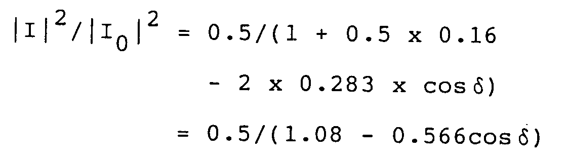
As a result, the intensity ratio ranges from 30.4 to 97.3% according to the value of cos δ. - When the transmittance T of the light-absorbing
film 32 is 25%, and the reflectance R of the opticalsemitransparent film 25 is 20%, the intensity ratio is obtained by:
As a result, the intensity ratio ranges from 18.3 to 21.9% according to the value of cos δ. - When the transmittance T of the light-absorbing
film 32 is 11.1%, and the reflectance R of the opticalsemitransparent film 25 is 10%, the intensity ratio is obtained by:
As a result, the intensity ratio ranges from 9.7 to 10.2% according to the value of cos δ. - In the above calculations, the difference between the refractive indices of the
SiO₂ film 26 and theadhesive layer 27 is small, and the reflectance of the interface therebetween is small, i.e., 0.03%. For these reasons, the reflection of the interface isneglected. Furthermore, it is an assumption that a non-reflective coating is formed between aprism 15 and the opticalsemitransparent film 25. - As is apparent from the above results, variations in intensity ratio are smaller when the light-absorbing
film 32 is used than when the light-absorbingfilm 32 is not used. Therefore, according to this first embodiment, multiple interference is suppressed, and fringes are reduced. In addition, the opticalsemitransparent film 25 and the light-absorbingfilm 32 can be formed on theprism 15 in mass production. An optical optimal point can coincide with a signal optimal point, thereby improving playability. - On the other hand, in this first embodiment, unlike the above prior art, an
SiN film 31 and theSiO₂ film 26 each having a high-precision thickness need not be formed. Thephotodiodes - Although the
light absorbing film 32 is independently used in the above first embodiment, theadhesive layer 27 may contain a dye to add the function of a light-absorbing film to theadhesive layer 27. - The second embodiment of the present invention applied to an optomagnetic recording laser coupler will be described below with reference to Figs. 8A and 8B.
- As shown in Fig. 8A, in an optomagnetic
recording laser coupler 61 to which the second embodiment is applied, twophotodiodes Si substrate 62. As shown in Fig. 8B, thephotodiode 63 is constituted by three parts A to C divided in a direction perpendicular to the alignment direction of thephotodiodes photodiode 64 is constituted by three parts D to F divided in the direction of the parts A to C. - A
polarizing film 65 is formed on the entire upper surface of theSi substrate 62. Thispolarizing film 65 transmits only a P-polarized light component and reflects an S-polarized light component. Amicroprism 66 having a trapezoidal section, a height of about 1 mm, and a surface inclined at an angle of 45° is adhered on thepolarizing film 65 above thephotodiodes - Although the
polarizing film 65 is formed on the entire upper surface of theSi substrate 62, thepolarizing film 65 may be formed on the entire lower surface of themicroprism 66. Furthermore, thepolarizing film 65 may be formed on only the upper surface portions of theSi substrate 62 which correspond to the upper portions of thephotodiodes polarizing film 65 may be formed on the lower surface portions of themicroprism 66 which correspond to thephotodiodes - A λ/4
plate 67 is adhered on the upper surface of themicroprism 66, and atotal reflection film 68 is formed on the λ/4plate 67. In addition, an unpolarizing film 71 having a reflectance of 50% is formed on the inclined surface of themicroprism 66. Note that a phase film using a polymer film having uniform orientation may be used in place of the λ/4plate 67. - As described above, an optomagnetic recording polarization
optical system 72 according to the second embodiment is formed. In order to constitute the optomagneticrecording laser coupler 61, anSi substrate 73 other than theSi substrate 62 is fixed by a silver paste or the like on thepolarizing film 65 at a position opposite to the inclined surface of themicroprism 66. - A
photodiode 74 is formed on the upper surface of theSi substrate 73, and alaser diode 75 is fixed on the upper surface of theSi substrate 73 by soldering or the like. In addition, anoptomagnetic recording pickup 77 is constituted by the above optomagneticrecording laser coupler 61 and anobjective lens 76. - In the
optomagnetic recording pickup 77 with the above arrangement, light 78 emitted from thelaser diode 75 is polarized light having an electric field component inclined at 45° with respect to the incident surface of thepolarizing film 65. The light 78 is incident on the unpolarizing film 71, and only 50% of the light 78 is reflected upward. Thephotodiode 74 is used to directly monitor light emitted backward from thelaser diode 75 and to control the amount of a current injected into thelaser diode 75. - The light 78 reflected by the unpolarizing film 71 is focused by the
objective lens 76 on anoptomagnetic disk 79, and the polarization plane of the light is rotated in accordance with a magnetic signal recorded on theoptomagnetic disk 79. The light 78 reflected by theoptomagnetic disk 79 is incident on the unpolarizing film 71 again, and 50% of the reflectedlight 78 is transmitted through the unpolarizing film 71. - The light 78 transmitted through the unpolarizing film 71 propagates through the
microprism 66 and is incident on thepolarizing film 65. Only the P-polarized light component of the light 78 incident on thepolarizing film 65 is transmitted through thepolarizing film 65 and is incident on thephotodiode 63, and the S-polarized light component of the light 78 is reflected by thepolarizing film 65. - The light 78 reflected by the
polarizing film 65 propagates through themicroprism 66, is transmitted through the λ/4plate 67, and is incident on thetotal reflection film 68. The light 78 is reflected by thetotal reflection film 68 and transmitted through the λ/4plate 67 again. That is, the light 78 is reciprocated in the λ/4plate 67 to be converted into a P-polarized light component. - The light 78 reflected by the
total reflection film 68 propagates through themicroprism 66 and is incident on thepolarizing film 65. However, since the light 78 is converted into the P-polarized light component as described above, the P-polarized light component is transmitted through thepolarizing film 65 and is incident on thephotodiode 64. Therefore, an optomagnetic signal is obtained by differential detection expressed by:

In addition, when theoptomagnetic recording pickup 77 and theoptomagnetic disk 79 are set in an in-focus state, as shown in Fig. 8A, the light 78 is focused on thetotal reflection film 68. For this reason, a focus error signal can be obtained by differential detection expressed by:

Therefore, the rotation of the polarization plane of light reflected by the optomagnetic recording-medium can be detected by a differential output from the first and second light-receiving elements, and an optomagnetic recording pickup can be formed. In addition, since assembling at the same level as that of a semiconductor chip can be performed, a compact, thin optomagnetic recording pickup can be formed. - The third embodiment of the present invention will be described below. As shown in Fig. 10, in a pickup for reading an optomagnetic recording signal from an
optomagnetic disk 82, an optomagneticrecording laser coupler 81 is constituted by integrating optical elements other than anobjective lens 83. - As shown in Fig. 9, the optomagnetic
recording laser coupler 81 includes anSi substrate 84. Asubmount 85 serving as another Si substrate is fixed on theSi substrate 84 by a silver paste or the like, and alaser diode 86 is fixed on thesubmount 85 by soldering or the like. - Two
photodiodes Si substrate 84 at positions different from the position where thesubmount 85 is fixed. As shown in Fig. 8B, thephotodiode 87 is constituted by three parts A to C divided in a direction perpendicular to the alignment direction of thephotodiodes photodiode 88 is constituted by three parts D to F divided in the direction of the parts A to C. - A
prism 91 having a parallelogram side section and a height of about 1 mm is adhered to thephotodiodes polarization beam splitter 92 which reflects 100% of an S-polarized light component and transmits 100% of a P-polarized light component is formed on an inclined surface of theprism 91 opposite to thephotodiode 87, and atotal reflection mirror 93 is formed on the inclined surface opposite to the inclined surface on which thepolarization beam splitter 92 is formed. - A λ/2
plate 94 and apolarization beam splitter 95 which reflects an S-polarized light component within a range of 1 to 100%, in a normal state, 20 to 80%, and transmits 100% of a P-polarized light component are integrally fixed on the upper surface of theprism 91 above thephotodiode 87. Note that the reflectance for an S-polarized light component in thepolarization beam splitter 95 is determined by a ratio of the intensity of the S-polarized light component returned from theoptomagnetic disk 82 to the intensity of the P-polarized light component serving as a signal component, i.e., the degree of enhancement of the signal. - In addition, a stray
light protecting film 96 serving as a light-absorbing film or a reflecting film is formed on the upper surface of theprism 91 at a position wherein the λ/2plate 94 is not formed. All the above optical elements fixed on theSi substrate 84 are sealed in apackage 97. A transparent window (not shown) is formed at a portion of thepackage 97 above thepolarization beam splitter 95. - In the third embodiment, as shown in Fig. 11, light 98 emitted from the
laser diode 86 is an S-polarized light component having an electric field component polarized perpendicularly to the drawing surface in Fig. 11. This light 98 is incident on thepolarization beam splitter 95, and only part of the light 98 is reflected upward. - The light 98 reflected by the
polarization beam splitter 95, as shown in Fig. 10, is focused on theoptomagnetic disk 82 by theobjective lens 83, and the polarization plane of the light 98 is rotated by about ±0.3° in accordance with a magnetic signal recorded on theoptomagnetic disk 82. - As a result, although 100% of the light 98 incident on the
optomagnetic disk 82 is an S-polarized light component, 0.5% of the light 98 reflected by theoptomagnetic disk 82, i.e., 0.5% of the light 98 returned from theoptomagnetic disk 82, is a P-polarized light component as a signal component. The P-polarized light component has an electric field component polarized parallel to the drawing surface in Fig. 10. - The light 98 returning from the
optomagnetic disk 82 is incident on thepolarization beam splitter 95 again, 100% of the P-polarized light component serving as the signal component of the light 98 is transmitted through thepolarization beam splitter 95, and only part of the S-polarized light component of the light 98 is transmitted through thepolarization beam splitter 95. - The light 98 transmitted through the
polarization beam splitter 95 is incident on the λ/2plate 94, and the polarization direction of the light 98 is rotated through 45° by the λ/2plate 94. As shown in Fig. 12, of the light 98 which has the polarization direction rotated through 45° by the λ/2plate 94, is incident on theprism 91, and reaches thepolarization beam splitter 92, the P-polarized light component is transmitted through thepolarization beam splitter 92, and the S-polarized light component is reflected by thepolarization beam splitter 92. - The light 98 transmitted through the
polarization beam splitter 92 is incident on thephotodiode 87. The light 98 reflected by thepolarization beam splitter 92 is focused in theprism 91 once, is reflected by thetotal reflection mirror 93, and is incident on thephotodiode 88. That is, components of the light 98 which are not modulated by theoptomagnetic disk 82 are split to thephotodiodes - For this reason, as in the second embodiment in Fig. 8B, a focus error signal is obtained by differential detection expressed by:

In addition, an optomagnetic signal can be obtained by differential detection expressed by:

Figs. 13 and 14 show two modifications of the third embodiment. In each of these modifications, thepolarization beam splitter 92 which reflects 100% of an S-polarized light component and transmits 100% of a P-polarized light component is arranged, and the light 98 returned from theoptomagnetic disk 82 are split into light components before and after the focal point of the light 98. Therefore, a focus error signal can be differentially detected, and the same function as that of the third embodiment can be obtained. - Fig. 15 shows the fourth embodiment. According to the fourth embodiment, a
photodiode 101 for directly monitoring an emission output from alaser diode 86 to control the amount of a current injected in thelaser diode 86 is formed on anSi substrate 84, and ahalf mirror 102 for guidinglight 98 to thephotodiode 101 is arranged. The fourth embodiment has the almost same arrangement as that of the third embodiment shown in Fig. 9 except for the above-described arrangement. Note that thephotodiode 101 may be adhered to apolarization beam splitter 95 or aprism 91. In this case, thehalf mirror 102 is not required. - As has been described above, according to the present invention, in a pickup used in an unpolarization or polarization optical system recording scheme, a laser coupler in which the amounts of light incident on two or more photodiodes are properly controlled to preferably perform differential detection can be obtained.
Claims (9)
- An optical apparatus, having an optical semitransparent film formed on a light-receiving element, for causing said light-receiving element to receive part of light incident on said optical semitransparent film, comprising
a light-absorbing film formed between said light-receiving element and said optical semitransparent film. - An optical apparatus having a structure in which a plurality of light-receiving elements are arranged on a substrate, a prism is fixed on said plurality of light-receiving elements, and an optical semitransparent film is formed between said light-receiving elements and said prism, comprising
a light-absorbing film formed between said light-receiving element and said optical semitransparent film. - An optical apparatus having a structure in which a plurality of light-receiving elements are arranged on a substrate, a prism is fixed on said plurality of light-receiving elements through an adhesive layer, and an optical semitransparent film is formed between at least one of said light-receiving elements and said prism, comprising
a light-absorbing film formed between said light-receiving element and said optical semitransparent film. - An optical apparatus having a structure in which a plurality of light-receiving elements are arranged on a substrate, a prism is fixed on said plurality of light-receiving elements through an adhesive layer, and an optical semitransparent film is formed between at least one of said light-receiving elements and said prism,
wherein said adhesive layer interposed between said light-receiving elements and said optical semitransparent film has light absorbance. - An apparatus according to claim 4,
wherein said adhesive layer interposed between said light-receiving elements and said optical semitransparent film contains a dye to have light absorbance. - An optomagnetic recording polarization optical apparatus in which light is radiated on an optomagnetic recording medium to detect rotation of a polarization plane of reflected light of the light, thereby reading recorded data,
wherein a prism for guiding the reflected light component to a light-receiving element and said light-receiving element are formed on the same substrate. - An apparatus according to claim 6, comprising:
first and second light-receiving elements formed on said semiconductor substrate;
a polarizing film, formed on at least said first and second light-receiving elements, for transmitting a first light component serving as a linearly polarized light component and for reflecting a second light component serving as a linear polarized light component having a polarization plane perpendicular to that of the first light component;
a prism arranged on said polarizing film;
a λ/4 plate arranged on a surface of said prism opposite to a surface on which said polarizing film is formed; and
a total reflection film formed on said λ/4 plate. - An optomagnetic recording polarization optical apparatus comprising:
a laser diode, fixed on a semiconductor substrate, for emitting a first light component serving as a linear polarized light component;
a first polarization beam splitter, fixed on said semiconductor substrate, for reflecting at least part of the first light component and transmitting a second light component serving as a linear polarized light component having a polarization plane perpendicular to that of the first light component;
a λ/2 plate, fixed on said semiconductor substrate, for causing a light component transmitted through said first polarization beam splitter to be incident on said λ/2 plate;
a second polarization beam splitter, fixed on said semiconductor substrate, for reflecting the first light component, transmitting the second light component, and causing a light component transmitted through said λ/2 plate to be incident on said second polarization beam splitter;
a prism, fixed on said semiconductor substrate, for causing the light component reflected by said second polarization beam splitter to be incident on said prism and to be focused; and
first and second light-receiving elements, formed on said semiconductor substrate, for causing the light component transmitted through said second polarization beam splitter and the focused light component to be incident on said first and second light-receiving elements, respectively. - An optomagnetic recording polarization optical apparatus comprising:
a laser diode, fixed on a semiconductor substrate, for emitting a first light component serving as a linear polarized light component;
a first polarization beam splitter, fixed on said semiconductor substrate, for reflecting at least part of the first light component and transmitting a second light component serving as a linear polarized light component having a polarization plane perpendicular to that of the first light component;
a λ/2 plate, fixed on said semiconductor substrate, for causing a light component transmitted through said first polarization beam splitter to be incident on said λ/2 plate;
a second polarization beam splitter, fixed on said semiconductor substrate, for reflecting the first light component, transmitting the second light component, and causing a light component transmitted through said λ/2 plate to be incident on said second polarization beam splitter;
a prism, fixed on said semiconductor substrate, for causing the light component reflected by said second polarization beam splitter to be incident on said prism and to be focused;
first and second light-receiving elements, formed on said semiconductor substrate, for causing the light component transmitted through said second polarization beam splitter and the focused light component to be incident on said first and second light-receiving elements, respectively,
a half mirror, fixed on said semiconductor substrate, for reflecting part of output light from said laser diode for emitting the first light component serving as the linear polarized light component; and
a third light-emitting element, formed on said semiconductor substrate, for causing the first light component reflected by said half mirror to be incident on said third light-emitting element.
Priority Applications (2)
| Application Number | Priority Date | Filing Date | Title |
|---|---|---|---|
| EP97120975A EP0836177B1 (en) | 1991-12-27 | 1992-12-24 | Optical apparatus |
| EP97120974A EP0840305B1 (en) | 1991-12-27 | 1992-12-24 | Optical apparatus |
Applications Claiming Priority (6)
| Application Number | Priority Date | Filing Date | Title |
|---|---|---|---|
| JP359406/91 | 1991-12-27 | ||
| JP3359406A JP3057278B2 (en) | 1991-12-27 | 1991-12-27 | Optical device |
| JP30044/92 | 1992-01-21 | ||
| JP4030044A JPH05198030A (en) | 1992-01-21 | 1992-01-21 | Laser coupler for magnetooptical recording |
| JP03420592A JP3355607B2 (en) | 1992-01-24 | 1992-01-24 | Polarizing optical system for magneto-optical recording |
| JP34205/92 | 1992-01-24 |
Related Child Applications (2)
| Application Number | Title | Priority Date | Filing Date |
|---|---|---|---|
| EP97120974A Division EP0840305B1 (en) | 1991-12-27 | 1992-12-24 | Optical apparatus |
| EP97120975A Division EP0836177B1 (en) | 1991-12-27 | 1992-12-24 | Optical apparatus |
Publications (3)
| Publication Number | Publication Date |
|---|---|
| EP0550036A2 true EP0550036A2 (en) | 1993-07-07 |
| EP0550036A3 EP0550036A3 (en) | 1993-09-22 |
| EP0550036B1 EP0550036B1 (en) | 1998-10-21 |
Family
ID=27286814
Family Applications (3)
| Application Number | Title | Priority Date | Filing Date |
|---|---|---|---|
| EP97120974A Expired - Lifetime EP0840305B1 (en) | 1991-12-27 | 1992-12-24 | Optical apparatus |
| EP92122003A Expired - Lifetime EP0550036B1 (en) | 1991-12-27 | 1992-12-24 | Optical apparatus |
| EP97120975A Expired - Lifetime EP0836177B1 (en) | 1991-12-27 | 1992-12-24 | Optical apparatus |
Family Applications Before (1)
| Application Number | Title | Priority Date | Filing Date |
|---|---|---|---|
| EP97120974A Expired - Lifetime EP0840305B1 (en) | 1991-12-27 | 1992-12-24 | Optical apparatus |
Family Applications After (1)
| Application Number | Title | Priority Date | Filing Date |
|---|---|---|---|
| EP97120975A Expired - Lifetime EP0836177B1 (en) | 1991-12-27 | 1992-12-24 | Optical apparatus |
Country Status (5)
| Country | Link |
|---|---|
| US (2) | US5350917A (en) |
| EP (3) | EP0840305B1 (en) |
| KR (2) | KR100263863B1 (en) |
| DE (3) | DE69227357T2 (en) |
| TW (1) | TW302101U (en) |
Cited By (9)
| Publication number | Priority date | Publication date | Assignee | Title |
|---|---|---|---|---|
| EP0729143A2 (en) * | 1995-02-24 | 1996-08-28 | Sony Corporation | Optical device |
| EP0731456A2 (en) * | 1995-03-04 | 1996-09-11 | Sony Corporation | Optical pickup and optical recording medium reproducing apparatus |
| EP0749119A2 (en) * | 1995-05-31 | 1996-12-18 | Daewoo Electronics Co., Ltd | Optical pickup apparatus |
| EP0750297A2 (en) * | 1995-06-23 | 1996-12-27 | Sony Corporation | Optical pickup and opto-magnetic signal reproducing apparatus |
| EP0713212A3 (en) * | 1994-11-17 | 1997-03-05 | Canon Kk | Optical information recording and reproducing apparatus |
| EP0810589A2 (en) * | 1996-05-27 | 1997-12-03 | Sony Corporation | Optical pickup device with a plurality of laser couplers |
| US5732060A (en) * | 1995-03-04 | 1998-03-24 | Sony Corporation | Optical pickup and optical recording medium reproducing apparatus having a wire grid unit |
| US6504812B2 (en) | 1996-05-27 | 2003-01-07 | Sony Corporation | Optical pickup device with a plurality of laser couplers |
| US7038994B1 (en) | 1996-05-27 | 2006-05-02 | Sony Corporation | Optical pickup device with a plurality of laser couplers |
Families Citing this family (21)
| Publication number | Priority date | Publication date | Assignee | Title |
|---|---|---|---|---|
| US5729511A (en) | 1991-02-15 | 1998-03-17 | Discovision Associates | Optical disc system having servo motor and servo error detection assembly operated relative to monitored quad sum signal |
| US6236625B1 (en) | 1991-02-15 | 2001-05-22 | Discovision Associates | Optical disc system having current monitoring circuit with controller for laser driver and method for operating same |
| US5677899A (en) | 1991-02-15 | 1997-10-14 | Discovision Associates | Method for moving carriage assembly from initial position to target position relative to storage medium |
| US5517479A (en) * | 1993-03-26 | 1996-05-14 | Matsushita Electronics Corporation | Optical head including a semiconductor laser having a non-scatter incident area |
| US5600619A (en) * | 1993-09-27 | 1997-02-04 | Seiko Epson Corporation | Optical head |
| JP3379814B2 (en) * | 1993-11-19 | 2003-02-24 | オリンパス光学工業株式会社 | Light head |
| US5598394A (en) * | 1994-05-19 | 1997-01-28 | Sanyo Electric Co., Ltd. | Optical pick-up |
| JPH0845102A (en) * | 1994-07-28 | 1996-02-16 | Olympus Optical Co Ltd | Optical head |
| JP3438365B2 (en) * | 1994-11-29 | 2003-08-18 | ソニー株式会社 | Composite optical device and method of manufacturing the same |
| US6434087B1 (en) | 1995-01-25 | 2002-08-13 | Discovision Associates | Optical disc system and method for controlling bias coil and light source to process information on a storage medium |
| JP3520594B2 (en) * | 1995-03-02 | 2004-04-19 | ソニー株式会社 | Compound optical device |
| US5727111A (en) * | 1995-06-19 | 1998-03-10 | Sony Corporation | Optical pick-up and light detecting cover therefor |
| JPH1019768A (en) * | 1996-03-19 | 1998-01-23 | Texas Instr Inc <Ti> | Surface plasmon resonance sensor |
| GB2315910A (en) * | 1996-07-31 | 1998-02-11 | Daewoo Electronics Co Ltd | Optical pickup system for reading information recorded on an optical disk |
| JPH10320810A (en) * | 1997-05-22 | 1998-12-04 | Sankyo Seiki Mfg Co Ltd | Semiconductor laser device and optical pickup device |
| DE19748324C2 (en) * | 1997-10-31 | 1999-08-26 | Siemens Ag | Optoelectronic sensor module |
| JP2001332799A (en) * | 2000-05-19 | 2001-11-30 | Rohm Co Ltd | Molded semiconductor laser |
| JP3552042B2 (en) * | 2001-05-15 | 2004-08-11 | 船井電機株式会社 | Fixing method of optical pickup and plate with electronic components |
| JP4322058B2 (en) * | 2003-07-23 | 2009-08-26 | 日本電産サンキョー株式会社 | Optical element fixing structure and optical head device |
| JP2005106879A (en) * | 2003-09-29 | 2005-04-21 | Minolta Co Ltd | Method for manufacturing prism having multilayer film on surface |
| JP2005235276A (en) * | 2004-02-18 | 2005-09-02 | Tdk Corp | Optical head, optical reproducing apparatus, and optical recording/reproducing apparatus |
Citations (4)
| Publication number | Priority date | Publication date | Assignee | Title |
|---|---|---|---|---|
| EP0278406A2 (en) * | 1987-02-06 | 1988-08-17 | Sony Corporation | Optical pickup head |
| JPH01237939A (en) * | 1988-03-18 | 1989-09-22 | Sony Corp | Optical pickup device |
| JPH01315036A (en) * | 1988-03-18 | 1989-12-20 | Sony Corp | Optical pickup device |
| EP0439876A1 (en) * | 1990-01-29 | 1991-08-07 | Hitachi Maxell Ltd. | Optical head with a double-beam splitter |
Family Cites Families (10)
| Publication number | Priority date | Publication date | Assignee | Title |
|---|---|---|---|---|
| US4262198A (en) * | 1979-07-30 | 1981-04-14 | California Institute Of Technology | Broadband optical radiation detector |
| JPS56107247A (en) * | 1980-01-31 | 1981-08-26 | Ricoh Co Ltd | Image recording method |
| US4695719A (en) * | 1983-12-05 | 1987-09-22 | Honeywell Inc. | Apparatus and method for opto-electronic package |
| JPS60131648A (en) * | 1983-12-19 | 1985-07-13 | Toshiba Corp | Optical head |
| EP0226647B1 (en) * | 1985-12-17 | 1991-05-29 | Ibm Deutschland Gmbh | Read/write head for optical disks |
| JPH0719394B2 (en) * | 1986-04-23 | 1995-03-06 | ソニー株式会社 | Semiconductor laser device |
| EP0339722B1 (en) * | 1988-04-26 | 1993-10-06 | Koninklijke Philips Electronics N.V. | Arrangement for optically scanning a magneto-optical carrier |
| JPH04149840A (en) * | 1990-10-12 | 1992-05-22 | Olympus Optical Co Ltd | Optical information reader |
| JPH04177643A (en) * | 1990-11-13 | 1992-06-24 | Olympus Optical Co Ltd | Optical apparatus for reproducing information |
| JPH04289541A (en) * | 1991-01-10 | 1992-10-14 | Olympus Optical Co Ltd | Magneto-optical pickup device |
-
1992
- 1992-12-23 US US07/996,149 patent/US5350917A/en not_active Expired - Fee Related
- 1992-12-24 TW TW085207967U patent/TW302101U/en unknown
- 1992-12-24 EP EP97120974A patent/EP0840305B1/en not_active Expired - Lifetime
- 1992-12-24 DE DE69227357T patent/DE69227357T2/en not_active Expired - Fee Related
- 1992-12-24 EP EP92122003A patent/EP0550036B1/en not_active Expired - Lifetime
- 1992-12-24 DE DE69232508T patent/DE69232508D1/en not_active Expired - Lifetime
- 1992-12-24 KR KR1019920025345A patent/KR100263863B1/en not_active IP Right Cessation
- 1992-12-24 EP EP97120975A patent/EP0836177B1/en not_active Expired - Lifetime
- 1992-12-24 DE DE69232509T patent/DE69232509D1/en not_active Expired - Lifetime
-
1994
- 1994-01-11 US US08/179,914 patent/US5396061A/en not_active Expired - Fee Related
-
2000
- 2000-04-19 KR KR1020000020755A patent/KR100280055B1/en not_active IP Right Cessation
Patent Citations (4)
| Publication number | Priority date | Publication date | Assignee | Title |
|---|---|---|---|---|
| EP0278406A2 (en) * | 1987-02-06 | 1988-08-17 | Sony Corporation | Optical pickup head |
| JPH01237939A (en) * | 1988-03-18 | 1989-09-22 | Sony Corp | Optical pickup device |
| JPH01315036A (en) * | 1988-03-18 | 1989-12-20 | Sony Corp | Optical pickup device |
| EP0439876A1 (en) * | 1990-01-29 | 1991-08-07 | Hitachi Maxell Ltd. | Optical head with a double-beam splitter |
Non-Patent Citations (2)
| Title |
|---|
| PATENT ABSTRACTS OF JAPAN vol. 16, no. 493 (P-1435)13 October 1992 & JP-A-04 177 643 ( OLYMPUS OPTICAL CO ) 24 June 1992 * |
| PATENT ABSTRACTS OF JAPAN vol. 5, no. 113 (P-89)13 November 1981 & JP-A-56 107 247 ( RICOH CO ) 26 August 1981 * |
Cited By (21)
| Publication number | Priority date | Publication date | Assignee | Title |
|---|---|---|---|---|
| EP0713212A3 (en) * | 1994-11-17 | 1997-03-05 | Canon Kk | Optical information recording and reproducing apparatus |
| US5657305A (en) * | 1994-11-17 | 1997-08-12 | Canon Kabushiki Kaisha | Optical information recording and reproducing apparatus including a total reflection surface or a light shield plate disposed between a polarized light separating surface and a detection device for light beam compensation |
| US5703861A (en) * | 1995-02-24 | 1997-12-30 | Sony Corporation | Integrated confocal optical pick-up head with a hologram and a polarizer mounted on each side of a transparent heat sink |
| EP0729143A3 (en) * | 1995-02-24 | 1996-09-04 | Sony Corp | |
| EP0729143A2 (en) * | 1995-02-24 | 1996-08-28 | Sony Corporation | Optical device |
| EP0731456A2 (en) * | 1995-03-04 | 1996-09-11 | Sony Corporation | Optical pickup and optical recording medium reproducing apparatus |
| EP0731456A3 (en) * | 1995-03-04 | 1996-09-25 | Sony Corp | |
| US5732060A (en) * | 1995-03-04 | 1998-03-24 | Sony Corporation | Optical pickup and optical recording medium reproducing apparatus having a wire grid unit |
| US5953294A (en) * | 1995-05-31 | 1999-09-14 | Daewoo Electronics Co., Ltd. | Optical pickup apparatus |
| EP0749119A3 (en) * | 1995-05-31 | 1997-08-20 | Daewoo Electronics Co Ltd | Optical pickup apparatus |
| US5787058A (en) * | 1995-05-31 | 1998-07-28 | Daewoo Electronics Co., Ltd. | Optical pickup apparatus utilizing a polygonal prism |
| EP0749119A2 (en) * | 1995-05-31 | 1996-12-18 | Daewoo Electronics Co., Ltd | Optical pickup apparatus |
| EP0750297A3 (en) * | 1995-06-23 | 1998-01-07 | Sony Corporation | Optical pickup and opto-magnetic signal reproducing apparatus |
| EP0750297A2 (en) * | 1995-06-23 | 1996-12-27 | Sony Corporation | Optical pickup and opto-magnetic signal reproducing apparatus |
| EP0810589A2 (en) * | 1996-05-27 | 1997-12-03 | Sony Corporation | Optical pickup device with a plurality of laser couplers |
| EP0810589A3 (en) * | 1996-05-27 | 1998-07-01 | Sony Corporation | Optical pickup device with a plurality of laser couplers |
| US6091689A (en) * | 1996-05-27 | 2000-07-18 | Sony Corporation | Optical pickup device with a plurality of laser couplers |
| US6134208A (en) * | 1996-05-27 | 2000-10-17 | Sony Corporation | Optical pickup device with a plurality of laser couplers |
| US6504812B2 (en) | 1996-05-27 | 2003-01-07 | Sony Corporation | Optical pickup device with a plurality of laser couplers |
| EP1293973A3 (en) * | 1996-05-27 | 2004-10-13 | Sony Corporation | Optical pickup device with a plurality of laser couplers |
| US7038994B1 (en) | 1996-05-27 | 2006-05-02 | Sony Corporation | Optical pickup device with a plurality of laser couplers |
Also Published As
| Publication number | Publication date |
|---|---|
| KR100263863B1 (en) | 2000-08-16 |
| EP0840305A3 (en) | 1999-01-27 |
| US5396061A (en) | 1995-03-07 |
| DE69227357D1 (en) | 1998-11-26 |
| EP0840305A2 (en) | 1998-05-06 |
| EP0836177B1 (en) | 2002-03-20 |
| EP0550036B1 (en) | 1998-10-21 |
| EP0550036A3 (en) | 1993-09-22 |
| TW302101U (en) | 1997-04-01 |
| DE69232508D1 (en) | 2002-04-25 |
| EP0840305B1 (en) | 2002-03-20 |
| EP0836177A1 (en) | 1998-04-15 |
| US5350917A (en) | 1994-09-27 |
| KR100280055B1 (en) | 2001-01-15 |
| DE69232509D1 (en) | 2002-04-25 |
| DE69227357T2 (en) | 1999-06-02 |
Similar Documents
| Publication | Publication Date | Title |
|---|---|---|
| US5396061A (en) | Opto-magnetic recording polarization optical apparatus having a light absorbing film and a total reflection film | |
| US5155622A (en) | Polarizing optical element and device using the same | |
| US5621716A (en) | Optical pickup having a transparent lens member with two reflecting surfaces | |
| KR960007232B1 (en) | Optical pick-up head | |
| EP1184848A2 (en) | Optical pickup apparatus having an improved holographic unit, and optical disk drive including the same | |
| EP0608432B1 (en) | Polarizing element and optical element, and optical head | |
| KR950001875B1 (en) | Semiconductor laser apparatus | |
| JP3029541B2 (en) | Optical pickup device | |
| US6192020B1 (en) | Semiconductor laser device | |
| US20030169668A1 (en) | Magneto-optical pickup | |
| KR100449612B1 (en) | Optical pickup and opto-magnetic signal reproducing apparatus | |
| JPH06289321A (en) | Analyzer, optical element, photodetector, optical head, magneto-optical signal detecting means, position error signal detecting means, and manufacture of optical element | |
| US5566157A (en) | Optical pickup for information recording/reproducing apparatus having polygon prism, hologram, and grating lens | |
| EP0981063A2 (en) | Polarizer, optical element, and optical head | |
| JPH0636338A (en) | Optical pickup | |
| JP2001014715A (en) | Optical pickup device | |
| JPH08271712A (en) | Optical element and optical integrated circuit | |
| JPH05198030A (en) | Laser coupler for magnetooptical recording | |
| JPH07272310A (en) | Optical integrated circuit and optical pickup | |
| JPH09297935A (en) | Optical pickup device | |
| CN1182933A (en) | Size reduced compact disc picking up system | |
| JPH07182712A (en) | Optical pickup device | |
| JPH0469825A (en) | Photodetector | |
| JPH05182232A (en) | Optical device | |
| JPH09180284A (en) | Optical head |
Legal Events
| Date | Code | Title | Description |
|---|---|---|---|
| PUAI | Public reference made under article 153(3) epc to a published international application that has entered the european phase |
Free format text: ORIGINAL CODE: 0009012 |
|
| AK | Designated contracting states |
Kind code of ref document: A2 Designated state(s): DE FR GB NL |
|
| PUAL | Search report despatched |
Free format text: ORIGINAL CODE: 0009013 |
|
| AK | Designated contracting states |
Kind code of ref document: A3 Designated state(s): DE FR GB NL |
|
| 17P | Request for examination filed |
Effective date: 19940222 |
|
| 17Q | First examination report despatched |
Effective date: 19960404 |
|
| GRAG | Despatch of communication of intention to grant |
Free format text: ORIGINAL CODE: EPIDOS AGRA |
|
| GRAG | Despatch of communication of intention to grant |
Free format text: ORIGINAL CODE: EPIDOS AGRA |
|
| GRAH | Despatch of communication of intention to grant a patent |
Free format text: ORIGINAL CODE: EPIDOS IGRA |
|
| RAP1 | Party data changed (applicant data changed or rights of an application transferred) |
Owner name: SONY CORPORATION |
|
| GRAH | Despatch of communication of intention to grant a patent |
Free format text: ORIGINAL CODE: EPIDOS IGRA |
|
| GRAA | (expected) grant |
Free format text: ORIGINAL CODE: 0009210 |
|
| AK | Designated contracting states |
Kind code of ref document: B1 Designated state(s): DE FR GB NL |
|
| REF | Corresponds to: |
Ref document number: 69227357 Country of ref document: DE Date of ref document: 19981126 |
|
| ET | Fr: translation filed | ||
| PLBE | No opposition filed within time limit |
Free format text: ORIGINAL CODE: 0009261 |
|
| STAA | Information on the status of an ep patent application or granted ep patent |
Free format text: STATUS: NO OPPOSITION FILED WITHIN TIME LIMIT |
|
| 26N | No opposition filed | ||
| REG | Reference to a national code |
Ref country code: GB Ref legal event code: IF02 |
|
| PGFP | Annual fee paid to national office [announced via postgrant information from national office to epo] |
Ref country code: GB Payment date: 20021218 Year of fee payment: 11 |
|
| PGFP | Annual fee paid to national office [announced via postgrant information from national office to epo] |
Ref country code: DE Payment date: 20021231 Year of fee payment: 11 |
|
| PGFP | Annual fee paid to national office [announced via postgrant information from national office to epo] |
Ref country code: NL Payment date: 20031205 Year of fee payment: 12 |
|
| PGFP | Annual fee paid to national office [announced via postgrant information from national office to epo] |
Ref country code: FR Payment date: 20031210 Year of fee payment: 12 |
|
| PG25 | Lapsed in a contracting state [announced via postgrant information from national office to epo] |
Ref country code: GB Free format text: LAPSE BECAUSE OF NON-PAYMENT OF DUE FEES Effective date: 20031224 |
|
| PG25 | Lapsed in a contracting state [announced via postgrant information from national office to epo] |
Ref country code: DE Free format text: LAPSE BECAUSE OF NON-PAYMENT OF DUE FEES Effective date: 20040701 |
|
| GBPC | Gb: european patent ceased through non-payment of renewal fee |
Effective date: 20031224 |
|
| PG25 | Lapsed in a contracting state [announced via postgrant information from national office to epo] |
Ref country code: NL Free format text: LAPSE BECAUSE OF NON-PAYMENT OF DUE FEES Effective date: 20050701 |
|
| PG25 | Lapsed in a contracting state [announced via postgrant information from national office to epo] |
Ref country code: FR Free format text: LAPSE BECAUSE OF NON-PAYMENT OF DUE FEES Effective date: 20050831 |
|
| NLV4 | Nl: lapsed or anulled due to non-payment of the annual fee |
Effective date: 20050701 |
|
| REG | Reference to a national code |
Ref country code: FR Ref legal event code: ST |