EP0545461A2 - Dispositif de récupération d'horloge - Google Patents
Dispositif de récupération d'horloge Download PDFInfo
- Publication number
- EP0545461A2 EP0545461A2 EP92203542A EP92203542A EP0545461A2 EP 0545461 A2 EP0545461 A2 EP 0545461A2 EP 92203542 A EP92203542 A EP 92203542A EP 92203542 A EP92203542 A EP 92203542A EP 0545461 A2 EP0545461 A2 EP 0545461A2
- Authority
- EP
- European Patent Office
- Prior art keywords
- data signal
- signal
- filter
- decided
- gate
- Prior art date
- Legal status (The legal status is an assumption and is not a legal conclusion. Google has not performed a legal analysis and makes no representation as to the accuracy of the status listed.)
- Granted
Links
Images

Classifications
-
- H—ELECTRICITY
- H04—ELECTRIC COMMUNICATION TECHNIQUE
- H04B—TRANSMISSION
- H04B1/00—Details of transmission systems, not covered by a single one of groups H04B3/00 - H04B13/00; Details of transmission systems not characterised by the medium used for transmission
- H04B1/69—Spread spectrum techniques
- H04B1/707—Spread spectrum techniques using direct sequence modulation
- H04B1/7073—Synchronisation aspects
- H04B1/7085—Synchronisation aspects using a code tracking loop, e.g. a delay-locked loop
-
- H—ELECTRICITY
- H04—ELECTRIC COMMUNICATION TECHNIQUE
- H04B—TRANSMISSION
- H04B1/00—Details of transmission systems, not covered by a single one of groups H04B3/00 - H04B13/00; Details of transmission systems not characterised by the medium used for transmission
- H04B1/69—Spread spectrum techniques
- H04B1/707—Spread spectrum techniques using direct sequence modulation
- H04B1/709—Correlator structure
Definitions
- the invention relates to a device for recovering a clock signal from a data signal with a data decoder clocked with the clock signal for obtaining a decided data signal from the data signal and with a voltage-controlled oscillator with an upstream loop filter for obtaining the clock signal from a control signal that can be derived from the data signal and the decided data signal .
- the invention further relates to a transmission system and a receiver with such a device.
- Devices of this type are required in receivers of digital message transmission systems in order to sample a transmitted data signal in the receiver with a clock signal.
- a device of the type mentioned is known.
- a received data signal is fed to a decision device and a delay / subtraction device, at whose output the difference signal is the difference between the data signal and a data signal delayed by one bit.
- the decision device is also supplied with the output signal of a voltage-controlled oscillator with an upstream loop filter as a clock signal.
- a signal obtained from the multiplication of the decided data signal and the difference signal is fed to the loop filter.
- the invention has for its object to provide a device of the type mentioned that simple Can be integrated in a manner that is also suitable for high frequencies.
- This object is achieved in a device of the type mentioned in the introduction that a DLL (delay-locked loop) correlation device is provided to obtain the control signal.
- a DLL delay-locked loop
- DLL correlation devices are used for the synchronization of code sequences and are, for example, from "Spread Spectrum Systems", p. 210 ff from RC Dixon, New York 1976 or from “The Delay-Locked Loop in Spread Spectrum Transmission: Analysis and Optimization ", selected work on communication systems No. 67, HW Schüssler, Er Weg known in 1988.
- a first input of the correlation device receives the data signal and a second input the output signal of the data decider, i.e. the decided data signal is fed.
- the clock signal is automatically set without adjustment or readjustment being necessary. This eliminates the need for time-consuming adjustment during the manufacture of the device.
- the device can be easily integrated with little effort.
- a correlation device which can be implemented in a cost-effective manner with gates, in particular EX-OR gates for correlation, is designed as a DLL delay correlator with two correlators, in each of which the data signal or the data signal delayed by a predefinable bit duration with the decided data signal or the decided one delayed by a predefinable bit duration Data signal is correlated, a difference generator being provided to obtain the control signal, which forms the control signal from the difference of signals at the output of the correlators.
- the data signal in two branches is correlated directly or time-shifted with the decided data signal directly or time-shifted.
- the predeterminable bit duration for the delay can be a multiple or even a fraction of the bit duration of the data signal.
- a generalized form of a DLL correlation device results if the correlation device is designed as a filter correlator with a first and a second filter, the data filter being able to be supplied to the first filter and the decided data signal being able to be supplied to the second filter, and the output signals of the filters being correlated with one another and the loop filter are fed.
- filter correlators are also selected from the code synchronization, for example from "Correlators with Analog Filter Pairs and Synthesis of Suitable Coding Signals for the Delay-Locked Loop", selected works on message systems No. 42, H.W. Schüssler, Er Weg known in 1980. This specifies conditions that lead to odd control characteristics.
- the data filter is supplied to the first filter in the correlation devices for clock synchronization and the decided data signal to the second filter.
- Square wave signals can be easily generated from the data signal are generated in that the data signal is fed to the correlation device via a limiter.
- a correlation device which can also be implemented in a simple manner has a first and a second EX-OR gate, the first EX-OR gate having the received data signal and the decided data signal and the second EX-OR gate a data signal delayed by one bit duration and the received data signal can be supplied and wherein the control signal is formed from the difference between the output signal of the first EX-OR gate and the output signal of the second EX-OR gate.
- the transmission system shown in FIG. 1 a consists of a transmitter 100, a receiver 101 and a transmission channel 103 through which the transmitter 100 and the receiver 101 are coupled to one another.
- a data signal 102 to be transmitted At the output of the transmitter 100 is a data signal 102 to be transmitted, which is supplied to the transmitter 101 via the transmission channel 103, so that a received data signal 104 is present at the input of the transmitter 101.
- the receiver 101 shown in FIG. 1a has a device for recovering a clock signal from the data signal 104, the function of which is explained in detail in connection with the following figures.
- reference character d is used for the received data signal designated by reference character 104 in FIG. 1a.
- FIG. 1b shows the basic arrangement of a device for clock recovery, which is based on a correlative method.
- a data signal d is fed to both a correlation device 14 and a data decider 11.
- a decided data signal e is also fed to the correlation device 14.
- a correlation signal k which controls a downstream voltage-controlled oscillator 12 via a loop filter 13.
- the voltage-controlled oscillator supplies a clock signal t for the data decider 11.
- a correlation takes place in the correlation device 14 the received data signal with the decided data signal e.
- the correlation signal k thus serves as an error signal for the retuning of the voltage-controlled oscillator.
- the received data signal d is thus correlated with the received data signal e, ie with an estimated value of the same data signal.
- Such a device for clock recovery has self-adjusting properties, since the regenerated clock signal is derived directly from the clock of the data signal d. As a result, the sampling phase is automatically updated in the data decider 11, so that complex adjustments and readjustments of the device are not required.
- FIG. 2 shows the basic illustration of a correlation device 14 which can be used for a device for clock recovery in accordance with the exemplary embodiment shown in FIG. 1.
- a received data signal d and a decided data signal e are fed to the correlation device 14.
- a control signal k is present at the output of the correlation device 14.
- the data signal d is fed to a first correlator K1 and a second correlator K2.
- the decided data signal e is likewise first fed to a second delay device 17b.
- the output signals of the delay devices 17a, 17b are forwarded to the correlators K1, K2.
- the correlators K1, K2 each consist of a multiplier and a downstream low-pass filter.
- the control signal k is present as the output signal k of the correlation device 14 as the difference signal.
- the correlation device shown in FIG. 2 is as DLL delay correlator designed.
- the received data signal d is correlated in two branches in the correlators K1, K2 directly or with a time shift with the decided data signal e directly or with a time shift.
- the difference between the output signals k1, k2 of the two correlators K1, K2 results in a superposition, so that finally a control signal k for controlling the voltage-controlled oscillator can be obtained.
- Such delay correlators can be implemented with gates, in particular EX-OR gates, with little effort, as is shown in FIG. 4a.
- FIG. 3 shows a further exemplary embodiment of a correlation device 14.
- the correlation device 14 is designed as a filter correlator with a first filter H1 and a second filter H2.
- the first filter H1 is supplied with the data signal d, the second filter H2 with the decided data signal e.
- a respectively filtered data signal h1 or decided data signal h2 is located at the output of the first H1 and the second H2 filter. Rules for these filters are "Correlators with Analog Filter Pairs and Synthesis of Appropriate Coding Signals for the Delay-Locked Loop", selected work on messaging systems No. 42, H.W. Schüssler, Er Weg, 1980 removable.
- the filtered signals h1, h2 are correlated with one another by means of a multiplier and a subsequent low-pass filtering. At the output of the low pass is the control signal k, which can be fed to the loop filter shown in FIG. 1.
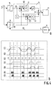
- FIG. 4a shows an exemplary embodiment of a device for clock recovery.
- a received data signal d is transmitted on the one hand via a limiter 15 of a correlation device 14 and on the other hand supplied to a data decider 11.
- a control signal k which controls a voltage-controlled oscillator 12 via a loop filter 13.
- the output signal of the voltage-controlled oscillator forms the clock signal t for clocking the data decider 11.
- a decided data signal e which is fed to the correlation device 14.
- the correlation device 14 consists of a first correlator 21 with an EX-OR gate and a downstream low-pass filter.
- the limited data signal and the decided data signal e are fed to the EX-OR gate.
- Correlation device 14 also has a second correlator 22 with a further EX-OR gate and a downstream low-pass filter.
- the EX-OR gate of the second correlator 22 is supplied with the data signal d delayed and limited by a bit duration Tb and the decided data signal e.
- the output signal of the first correlator 21 is delayed by half a bit duration and linked to the output signal of the second correlator 22 by forming a difference.
- the delay by half a bit duration T b / 2 can also be provided directly between the EX-OR gate and the low-pass filter of the first correlator 21. 4b, the signal curve for this embodiment is shown in track 6.
- FIG. 4b shows signal profiles of the device for clock recovery shown in FIG. 4a.
- the reference symbols surrounded by a circle in FIG. 4a correspond to the reference symbols used in FIG. 4b for identifying the signal profiles in tracks 1 to 7 also surrounded by a circle.
- Track 1 of the one shown in FIG. 4b shows an exemplary temporal course of the data signal d supplemented with the corresponding assignable logical values 1 or 0.
- Track 2 shows the output signal of the limiter shown in FIG. 4a.
- Track 3 shows the output signal of the voltage-controlled oscillator 12, ie the clock signal t formed from pulses, which marks the sampling times of the data decision maker.
- Track 4 shows the decided data signal e at the output of the data decider 11, which results from the received data signal d (track 1) by scanning with the clock or scan signal t shown in track 3.
- Track 5 shows the data signal delayed and limited by a bit duration Tb.
- Track 6 shows the output signal of the first correlator 21 delayed by half a bit duration, which is obtained from the limited data signal (track 2) and the received data signal e (track 4) by EX-OR operation.
- the time area is shown hatched, which is determined in the low-pass filtering, and the time area is shown cross-hatched, which results from the phase fluctuation of the data signal d shown in track 1.
- Track 7 finally shows the output signal of the second correlator 22, which is formed from an Ex-OR combination of the signal shown in track 5 and the received data signal (track 4).
- the time area that is determined in the low-pass filtering is also shown hatched in the signal shown in track 7, and the time area that is caused by phase fluctuations of the data signal shown in track 1 is shown cross-hatched.
- the delay by T b / 2 after the correlator 21 minimizes the interference AC voltage caused by the difference 23.
- Fig. 4a Based on the time profiles shown in Fig. 4b it is illustrated that with the help of those described in Fig. 4a Device for clock acquisition phase errors of the data signal can be compensated up to a maximum of plus / minus half a bit duration, ie the control range corresponds to 1T b . It is essential that in both signals of the track 6 and the track 7 supplied to the difference former 23, an opposite change in the mean value is taken into account. There is thus an automatic adjustment of the sampling phase of the clock signal t (track 3) without the need for a sampling phase adjustment or readjustment.
- the delay correlator shown in FIG. 4a can also be implemented in a simple manner in an integrated form.
Landscapes
- Engineering & Computer Science (AREA)
- Computer Networks & Wireless Communication (AREA)
- Signal Processing (AREA)
- Synchronisation In Digital Transmission Systems (AREA)
- Stabilization Of Oscillater, Synchronisation, Frequency Synthesizers (AREA)
Applications Claiming Priority (2)
| Application Number | Priority Date | Filing Date | Title |
|---|---|---|---|
| DE4138540 | 1991-11-23 | ||
| DE4138540 | 1991-11-23 |
Publications (3)
| Publication Number | Publication Date |
|---|---|
| EP0545461A2 true EP0545461A2 (fr) | 1993-06-09 |
| EP0545461A3 EP0545461A3 (en) | 1993-06-23 |
| EP0545461B1 EP0545461B1 (fr) | 1997-07-09 |
Family
ID=6445418
Family Applications (1)
| Application Number | Title | Priority Date | Filing Date |
|---|---|---|---|
| EP92203542A Expired - Lifetime EP0545461B1 (fr) | 1991-11-23 | 1992-11-18 | Dispositif de récupération d'horloge |
Country Status (4)
| Country | Link |
|---|---|
| EP (1) | EP0545461B1 (fr) |
| JP (1) | JPH05244138A (fr) |
| CA (1) | CA2083420A1 (fr) |
| DE (1) | DE59208683D1 (fr) |
Family Cites Families (2)
| Publication number | Priority date | Publication date | Assignee | Title |
|---|---|---|---|---|
| US4320515A (en) * | 1980-03-07 | 1982-03-16 | Harris Corporation | Bit synchronizer |
| US5062122A (en) * | 1988-09-28 | 1991-10-29 | Kenwood Corporation | Delay-locked loop circuit in spread spectrum receiver |
-
1992
- 1992-11-18 EP EP92203542A patent/EP0545461B1/fr not_active Expired - Lifetime
- 1992-11-18 DE DE59208683T patent/DE59208683D1/de not_active Expired - Fee Related
- 1992-11-20 CA CA002083420A patent/CA2083420A1/fr not_active Abandoned
- 1992-11-20 JP JP4311791A patent/JPH05244138A/ja active Pending
Also Published As
| Publication number | Publication date |
|---|---|
| DE59208683D1 (de) | 1997-08-14 |
| EP0545461A3 (en) | 1993-06-23 |
| EP0545461B1 (fr) | 1997-07-09 |
| JPH05244138A (ja) | 1993-09-21 |
| CA2083420A1 (fr) | 1993-05-24 |
Similar Documents
| Publication | Publication Date | Title |
|---|---|---|
| DE69313802T2 (de) | Empfangsgerät für ein bandgespreiztes Signal | |
| EP0012394B1 (fr) | Circuit récepteur pour la synchronisation d'un génerateur pseudo-aléatoire avec un signal de réception transmis par un êmetteur | |
| DE69021532T2 (de) | Digitalsignaldetektor mit variabler Bandbreite. | |
| DE3750265T2 (de) | Verfahren und gerät zur entzerrung in datenübertragungssystemen. | |
| DE2702959A1 (de) | Synchronisationssignal-wiedergewinnungsschaltung fuer grundband-datensignale | |
| EP0011699B1 (fr) | Circuit pour la mesure de la distorsion de phase de signaux digitaux et son utilisation | |
| DE2657914C2 (de) | Schaltungsanordnung zum Grobsynchronisieren von Trägersignalen und Taktsignalen mit Datensignalen in einem Datenempfänger | |
| DE68916899T2 (de) | Automatische Verstärkungsregelung für Frequenzsprungempfänger. | |
| DE60009678T2 (de) | Frequenznachlaufschleife und verfahren zum frquenznachlaufen | |
| EP0073400B1 (fr) | Régénérateur pour signaux digitaux à réaction quantifiée | |
| EP0006988A1 (fr) | Dispositif pour récupérer le signal d'horloge dans la transmission digitale des signaux | |
| EP0545461B1 (fr) | Dispositif de récupération d'horloge | |
| DE4193255C2 (de) | Verfahren zur Frequenzsynchronisation sowie mobiles Funktelefon zur Verwendung in einem TDMA-Typ zellularen Kommunikationssystem | |
| DE3249021C2 (fr) | ||
| EP0356549A1 (fr) | Procédé et circuit pour contrôler numériquement la phase des impulsions d'une horloge d'échantillonnage | |
| DE4236774A1 (de) | Schnurlos-Telekommunikationsgerät | |
| EP0540946B1 (fr) | Méthode pour la transmission digitale d'informations | |
| WO2003081807A1 (fr) | Dispositif et procede de regulation du moment d'emission d'un signal d'emission continu | |
| DE2720896C2 (de) | Schaltung zum Regeln der Ausgangsfrequenz eines Wobbeloszillators | |
| EP0472752A1 (fr) | Dispositif de commande à distance avec joint de transmission à spectre étendu | |
| DE10132403A1 (de) | Verfahren und Vorrichtung zur Taktrückgewinnung aus einem Datensignal | |
| DE10207315B4 (de) | Vorrichtung zur Datenrückgewinnung aus einem empfangenen Datensignal | |
| DE3139157A1 (de) | Pilotton-demodulator fuer den stereo-fernsehempfang | |
| DE102017202879B4 (de) | Verfahren zur drathlosen seriellen Datenübertragung | |
| DE60132415T2 (de) | Frequenzsynchronisierer, der sowohl analoge als auch digitale Regelsignale verwendendet |
Legal Events
| Date | Code | Title | Description |
|---|---|---|---|
| PUAI | Public reference made under article 153(3) epc to a published international application that has entered the european phase |
Free format text: ORIGINAL CODE: 0009012 |
|
| PUAL | Search report despatched |
Free format text: ORIGINAL CODE: 0009013 |
|
| AK | Designated contracting states |
Kind code of ref document: A2 Designated state(s): DE FR GB IT |
|
| AK | Designated contracting states |
Kind code of ref document: A3 Designated state(s): DE FR GB IT |
|
| 17P | Request for examination filed |
Effective date: 19931213 |
|
| GRAG | Despatch of communication of intention to grant |
Free format text: ORIGINAL CODE: EPIDOS AGRA |
|
| 17Q | First examination report despatched |
Effective date: 19960925 |
|
| GRAH | Despatch of communication of intention to grant a patent |
Free format text: ORIGINAL CODE: EPIDOS IGRA |
|
| GRAH | Despatch of communication of intention to grant a patent |
Free format text: ORIGINAL CODE: EPIDOS IGRA |
|
| GRAA | (expected) grant |
Free format text: ORIGINAL CODE: 0009210 |
|
| AK | Designated contracting states |
Kind code of ref document: B1 Designated state(s): DE FR GB IT |
|
| PG25 | Lapsed in a contracting state [announced via postgrant information from national office to epo] |
Ref country code: IT Free format text: LAPSE BECAUSE OF FAILURE TO SUBMIT A TRANSLATION OF THE DESCRIPTION OR TO PAY THE FEE WITHIN THE PRE;WARNING: LAPSES OF ITALIAN PATENTS WITH EFFECTIVE DATE BEFORE 2007 MAY HAVE OCCURRED AT ANY TIME BEFORE 2007. THE CORRECT EFFECTIVE DATE MAY BE DIFFERENT FROM THE ONE RECORDED.SCRIBED TIME-LIMIT Effective date: 19970709 Ref country code: GB Effective date: 19970709 Ref country code: FR Effective date: 19970709 |
|
| REF | Corresponds to: |
Ref document number: 59208683 Country of ref document: DE Date of ref document: 19970814 |
|
| EN | Fr: translation not filed | ||
| GBV | Gb: ep patent (uk) treated as always having been void in accordance with gb section 77(7)/1977 [no translation filed] |
Effective date: 19970709 |
|
| PLBE | No opposition filed within time limit |
Free format text: ORIGINAL CODE: 0009261 |
|
| 26N | No opposition filed | ||
| PG25 | Lapsed in a contracting state [announced via postgrant information from national office to epo] |
Ref country code: DE Free format text: LAPSE BECAUSE OF NON-PAYMENT OF DUE FEES Effective date: 19980801 |