EP0541024B1 - Magnetic field detecting circuit - Google Patents
Magnetic field detecting circuit Download PDFInfo
- Publication number
- EP0541024B1 EP0541024B1 EP92118704A EP92118704A EP0541024B1 EP 0541024 B1 EP0541024 B1 EP 0541024B1 EP 92118704 A EP92118704 A EP 92118704A EP 92118704 A EP92118704 A EP 92118704A EP 0541024 B1 EP0541024 B1 EP 0541024B1
- Authority
- EP
- European Patent Office
- Prior art keywords
- magnetic field
- circuit
- coil
- squid
- field detecting
- Prior art date
- Legal status (The legal status is an assumption and is not a legal conclusion. Google has not performed a legal analysis and makes no representation as to the accuracy of the status listed.)
- Expired - Lifetime
Links
Images


Classifications
-
- G—PHYSICS
- G01—MEASURING; TESTING
- G01R—MEASURING ELECTRIC VARIABLES; MEASURING MAGNETIC VARIABLES
- G01R33/00—Arrangements or instruments for measuring magnetic variables
- G01R33/02—Measuring direction or magnitude of magnetic fields or magnetic flux
- G01R33/035—Measuring direction or magnitude of magnetic fields or magnetic flux using superconductive devices
- G01R33/0354—SQUIDS
- G01R33/0356—SQUIDS with flux feedback
-
- Y—GENERAL TAGGING OF NEW TECHNOLOGICAL DEVELOPMENTS; GENERAL TAGGING OF CROSS-SECTIONAL TECHNOLOGIES SPANNING OVER SEVERAL SECTIONS OF THE IPC; TECHNICAL SUBJECTS COVERED BY FORMER USPC CROSS-REFERENCE ART COLLECTIONS [XRACs] AND DIGESTS
- Y10—TECHNICAL SUBJECTS COVERED BY FORMER USPC
- Y10S—TECHNICAL SUBJECTS COVERED BY FORMER USPC CROSS-REFERENCE ART COLLECTIONS [XRACs] AND DIGESTS
- Y10S505/00—Superconductor technology: apparatus, material, process
- Y10S505/825—Apparatus per se, device per se, or process of making or operating same
- Y10S505/842—Measuring and testing
- Y10S505/843—Electrical
- Y10S505/845—Magnetometer
- Y10S505/846—Magnetometer using superconductive quantum interference device, i.e. squid
Definitions
- the invention relates to a magnetic field detecting circuit according to the preamble of claim 1 which uses a Josephson device applied for a high sensitive magnetic sensor, a current meter, a displacement detector, a high-frequency signal amplifier and the like.
- Such a magnetic field detecting circuit is for example known from Applied Physics A, solids and surfaces, vol. A 47 (1988), no. 3, pages 285-289, and is schematically represented in Fig. 2 of the present application.
- Fig. 2 is a circuit diagram of an SQUID (RO-SQUID) using a conventional relaxation oscillation, where a resistor 2 and a coil 3 connected in series with each other are connected in parallel with a DC-SQUID 7.
- a magnetic field signal from an input coil 4 enters the DC-SQUID 7 to be converted into a critical current value, and an oscillating frequency is shifted, and then a magnetic field is detected.
- this invention has a structure including a magnetic field input circuit magnetically coupled with a coil in a relaxation oscillator, so an optimum design of the magnetic field detecting circuit is achieved independently for a parameter of the relaxation oscillator and a parameter of a receiving circuit of a magnetic field respectively.
- a control line for controlling an oscillation magnetically coupled with a Josephson device in the oscillator is added to enable a multi-channelization by a series connection of the Josephson devices.
- a signal is input from a magnetic field input circuit magnetically coupled with a coil of a relaxation oscillator oscillated by a bias current, and converts an oscillating frequency to detect a value of a input magnetic field.
- a bias current is set at a suitable value, a critical current value of the Josephson device is varied by a control line magnetically coupled to the Josephson device, thereby the control of the oscillation is available.
- Fig. 1 is a circuit diagram of a first embodiment according to the present invention.
- Fig. 2 is a conventional circuit diagram of the RO-SQUID.
- Fig. 3 is a circuit diagram of a second embodiment according to the present invention.
- Fig. 4 is an embodiment of a magnetic field detecting system according to the present invention.
- Fig. 5 is a circuit diagram of a third embodiment according to the present invention.
- Fig. 6 is a circuit diagram of a fourth embodiment according to the present invention.
- Fig. 7 is a circuit diagram of a fifth embodiment according to the present invention.
- Fig. 8 is a circuit diagram of a sixth embodiment according to the present invention.
- Fig. 9 is a circuit diagram of a seventh embodiment according to the present invention.
- Fig. 10 is an embodiment of a multi-channel magnetic-field detecting system according to the present invention.
- Fig. 1 is a circuit diagram of a first embodiment according to the invention.
- a oscillating frequency "f" generated across the Josephson device satisfies the following equation, f ⁇ (R/L)/(ln ⁇ (Ib-Icmin)/(Ib-Icmax) ⁇ ) where Ib represents a bias current 5 flowing into a circuit, Icmax and Icmin represent a maximum critical current and a minimum critical current of the Josephson device 1 respectively, L represents an inductance of a coil 3, and R represents a resistance of a resistor 2.
- the oscillating frequency "f" is varied depending on an amount of the flux, the magnetic flux being detected as a frequency variation.
- An oscillation amplitude is of a gap voltage of the Josephson device with a constant value.
- Fig. 3 shows a second embodiment according to the invention, where can be provided a higher sensitivity compared to the first embodiment through being applied by an RF-SQUID 9 formed of the Josephson device 6 and a superconductive loop, and by a feedback coil 8 respectively, in addition to the input coil 4 as a magnetic field input circuit.
- a design can be performed separately for a parameter of the oscillating circuit and for a parameter of an RF-SQUID for detecting the magnetic field. This facilitates the design and realizes an optimum design with a high sensitization compared to the conventional RO-SQUID.
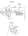
- Fig. 4 is an example of a magnetic field detecting system according to the invention, where the RF-SQUID 9 is applied a feedback operation by a feedback coil 8 for obtaining a larger dynamic range.
- a magnetic field inputted from a detecting coil 11 enters the input coil 4 to be input to the coil 3 through the RF-SQUID 9, thus an oscillating frequency of a relaxation oscillator can be varied.
- Oscillation wave forms are converted into a DC voltage through a head amplifier 12 and an F-V converter 13, after which only an amount of variations of the frequency is taken out by an integration amplifier 14 as an output signal and a part of the output signal is fed back.
- Fig. 5 shows a third embodiment according to the invention, showing a circuit in which a plurality of Josephson devices 1 of the second embodiment are connected in series with each other. Since an output of the relaxation oscillator is of a gap voltage of the Josephson device, the larger number of those connected in series with each other produces a larger amplitude to facilitate detection of a signal. This method is applied to the circuit of the first embodiment.
- FIG. 6 is a circuit diagram of a fourth embodiment, where the circuit of the first embodiment in Fig. 1 is multi-channelized. Two of the same magnetic-field detecting circuits are connected in series with each other to form two channels.
- An oscillation condition is, Icmax ⁇ Ib ⁇ ⁇ (Rn+R)/R ⁇ Icmin where Rn represents a normal conductive resistance of the Josephson device.
- a method according to the invention is to easily control, by the current of the control line 10, an oscillation of the circuit having multi-channels connected in series with each other, thus a magnetic field of each channel can be detected by sequentially monitoring a frequency of a voltage output there across in a manner of operating channel by channel. Wiring separately at every channel basis is not necessary, the number of wirings can be reduced, a cross talk between channels is prevented, this enables a more accurate measurement.
- Fig. 7 shows a fifth embodiment according to the invention, where a circuit is incorporated with a DC-SQUID 7 instead of the Josephson device 1 of the fourth embodiment (Fig. 6).
- the DC-SQUID 7 provides an easier control of the oscillation due to a smaller inductance and a larger variation amount of Icmax because it controls only an oscillation different from the conventional example in Fig. 2.
- Fig. 8 shows a sixth embodiment according to the invention, where is illustrated an example of the multi-channelization of the second embodiment (Fig. 3).
- Fig. 9 shows a seventh embodiment according to the invention, where a circuit is incorporated with a DC-SQUID 7 instead of the Josephson device 1 of the sixth embodiment.
- the DC-SQUID 7 is the same as in the fifth embodiment (Fig. 7).
- Fig. 10 shows an example of a multi-channel magnetic-field detecting system.
- a method of detecting a signal is the same as in Fig. 4, but there is added a shift register 15 in which the control line 10 for controlling the oscillation is controlled by an external clock signal 16.
- the shift register 15 can be produced by the superconductive circuit using the Josephson device, to be used in a superconductive state together with the magnetic field detecting circuit, and to be produced unitarily on the same substrate. In this system, an operation of each channel can be switched by the clock signal 16 to reduce the number of signal lines.
- the multi-channel magnetic-field detecting circuit connected in series with each other can be controlled their oscillations for one channel at a time to detect the signal, the magnetic field can be detected by less signal lines at a high efficiency.
- the embodiments has been shown and described for two channels, but more than two channels can be produced in a practical use.
- an input of the magnetic field is carried out from the coil 3 of the relaxation oscillator, this provides an optimum design and an easier control of the oscillation by the control line. Therefore, a multi-channelization can be realized in a high efficiency, a cross talk between the channels is prevented, and a result is that a more sensitive detection of the magnetic field can be provided.
Landscapes
- Physics & Mathematics (AREA)
- Condensed Matter Physics & Semiconductors (AREA)
- General Physics & Mathematics (AREA)
- Measuring Magnetic Variables (AREA)
- Superconductor Devices And Manufacturing Methods Thereof (AREA)
Applications Claiming Priority (2)
| Application Number | Priority Date | Filing Date | Title |
|---|---|---|---|
| JP291792/91 | 1991-11-07 | ||
| JP03291792A JP3081902B2 (ja) | 1991-11-07 | 1991-11-07 | 磁場検出回路 |
Publications (3)
| Publication Number | Publication Date |
|---|---|
| EP0541024A2 EP0541024A2 (en) | 1993-05-12 |
| EP0541024A3 EP0541024A3 (enExample) | 1994-01-12 |
| EP0541024B1 true EP0541024B1 (en) | 1997-04-09 |
Family
ID=17773491
Family Applications (1)
| Application Number | Title | Priority Date | Filing Date |
|---|---|---|---|
| EP92118704A Expired - Lifetime EP0541024B1 (en) | 1991-11-07 | 1992-11-01 | Magnetic field detecting circuit |
Country Status (4)
| Country | Link |
|---|---|
| US (1) | US5406201A (enExample) |
| EP (1) | EP0541024B1 (enExample) |
| JP (1) | JP3081902B2 (enExample) |
| DE (1) | DE69218883T2 (enExample) |
Cited By (1)
| Publication number | Priority date | Publication date | Assignee | Title |
|---|---|---|---|---|
| CN102288999A (zh) * | 2011-08-16 | 2011-12-21 | 中国地质科学院地球物理地球化学勘查研究所 | 高温超导弱磁测量传感器 |
Families Citing this family (12)
| Publication number | Priority date | Publication date | Assignee | Title |
|---|---|---|---|---|
| DE4317966C2 (de) * | 1993-05-28 | 2002-09-12 | Siemens Ag | Squid-Einrichtung mit einer supraleitenden Detektionsfläche |
| DE4323040A1 (de) * | 1993-07-09 | 1995-01-12 | Siemens Ag | Josephson-Sensoreinrichtung mit supraleitenden Teilen aus metalloxidischem Supraleitermaterial |
| DE19519517A1 (de) * | 1995-06-01 | 1996-12-05 | Forschungszentrum Juelich Gmbh | Mehrkanalsystem mit rf-SQUIDs |
| US6066948A (en) * | 1995-06-02 | 2000-05-23 | Seppae; Heikki | Squid magnetometer having resistor-capacitor damping circuits |
| KR0141758B1 (ko) * | 1995-08-25 | 1998-07-15 | 구자홍 | 초전도 양자간섭소자를 이용한 고주파신호 발생기 |
| DE19615254C2 (de) * | 1996-04-18 | 1999-03-11 | Diagnostikforschung Inst | Gerät zur höchstempfindlichen magnetischen Detektion von Analyten |
| KR100198534B1 (ko) * | 1996-05-02 | 1999-06-15 | 구자홍 | 두개의 초전도양자간섭소자를 이용한 자장측정장치 |
| US6321074B1 (en) | 1999-02-18 | 2001-11-20 | Itron, Inc. | Apparatus and method for reducing oscillator frequency pulling during AM modulation |
| KR100722755B1 (ko) * | 2006-04-14 | 2007-05-30 | 한국표준과학연구원 | 기준 접합을 갖는 이중이완발진 스퀴드의 특성조절 방법 |
| KR100774615B1 (ko) * | 2006-05-09 | 2007-11-12 | 한국표준과학연구원 | 이중이완발진 스퀴드의 기준전류 최적화 장치 |
| US9520180B1 (en) | 2014-03-11 | 2016-12-13 | Hypres, Inc. | System and method for cryogenic hybrid technology computing and memory |
| CN115438793B (zh) * | 2022-07-29 | 2024-08-13 | 本源量子计算科技(合肥)股份有限公司 | 一种量子芯片及其制备方法、量子计算机 |
Family Cites Families (3)
| Publication number | Priority date | Publication date | Assignee | Title |
|---|---|---|---|---|
| JPS60140164A (ja) * | 1983-12-28 | 1985-07-25 | Shimadzu Corp | スキツド磁力計 |
| US4689559A (en) * | 1984-11-13 | 1987-08-25 | Sperry Corporation | Apparatus and method to reduce the thermal response of SQUID sensors |
| JPH02257076A (ja) * | 1989-03-30 | 1990-10-17 | Fujitsu Ltd | ディジタルスクイド制御方式 |
-
1991
- 1991-11-07 JP JP03291792A patent/JP3081902B2/ja not_active Expired - Lifetime
-
1992
- 1992-10-28 US US07/967,723 patent/US5406201A/en not_active Expired - Fee Related
- 1992-11-01 EP EP92118704A patent/EP0541024B1/en not_active Expired - Lifetime
- 1992-11-01 DE DE69218883T patent/DE69218883T2/de not_active Expired - Fee Related
Cited By (2)
| Publication number | Priority date | Publication date | Assignee | Title |
|---|---|---|---|---|
| CN102288999A (zh) * | 2011-08-16 | 2011-12-21 | 中国地质科学院地球物理地球化学勘查研究所 | 高温超导弱磁测量传感器 |
| CN102288999B (zh) * | 2011-08-16 | 2013-05-15 | 中国地质科学院地球物理地球化学勘查研究所 | 高温超导弱磁测量传感器 |
Also Published As
| Publication number | Publication date |
|---|---|
| JPH0651041A (ja) | 1994-02-25 |
| DE69218883T2 (de) | 1997-07-24 |
| EP0541024A3 (enExample) | 1994-01-12 |
| JP3081902B2 (ja) | 2000-08-28 |
| DE69218883D1 (de) | 1997-05-15 |
| US5406201A (en) | 1995-04-11 |
| EP0541024A2 (en) | 1993-05-12 |
Similar Documents
| Publication | Publication Date | Title |
|---|---|---|
| EP0541024B1 (en) | Magnetic field detecting circuit | |
| US5045788A (en) | Digital SQUID control system for measuring a weak magnetic flux | |
| US4004217A (en) | Flux locked loop | |
| US5285155A (en) | Method and apparatus for magnetic flux locking based upon a history of plural comparisons of the SQUID output signal and a predetermined signal | |
| US5530349A (en) | Magnetic field sensor device using a flux-gate principle | |
| JP2662903B2 (ja) | 高感度磁場検出装置 | |
| US4866373A (en) | Superconducting current detecting circuit employing DC flux parametron circuit | |
| US4315215A (en) | Plural frequency type superconducting quantum interference fluxmeter | |
| EP0501241B1 (en) | Highly sensitive magnetic field detecting device | |
| US3696287A (en) | Superconducting constant voltage generator | |
| EP0846958A2 (en) | Voltage step up circuit for magnetometric sensor | |
| US5424641A (en) | SQUID fluxmeter having a pulse mulliplication circuit number for accurately measuring large rates of change in flux | |
| US3761798A (en) | Superconducting circuit means | |
| JPH0868834A (ja) | 超伝導磁力計 | |
| JPH06324130A (ja) | Squidセンサ装置 | |
| JP2869780B2 (ja) | ラッチフリーsquid磁束計 | |
| JP3156387B2 (ja) | Squid磁束計システム及びその初期値設定方法 | |
| JPH03131781A (ja) | Squid磁束計計測システム | |
| JPH07154147A (ja) | 超伝導発振器 | |
| JPH0694815A (ja) | Squid磁束計の動作点設定システム及び方法 | |
| JPH0654347B2 (ja) | 磁束計 | |
| Podt et al. | Digital squids based on smart dros | |
| KR100239492B1 (ko) | 다 채널 자장 측정 장치 및 그 방법 | |
| Makie‐Fukuda et al. | Automatic adjustment of bias current for direct current superconducting quantum interference device | |
| JP2782901B2 (ja) | スクイッド磁束計 |
Legal Events
| Date | Code | Title | Description |
|---|---|---|---|
| PUAI | Public reference made under article 153(3) epc to a published international application that has entered the european phase |
Free format text: ORIGINAL CODE: 0009012 |
|
| AK | Designated contracting states |
Kind code of ref document: A2 Designated state(s): DE GB IT NL |
|
| PUAL | Search report despatched |
Free format text: ORIGINAL CODE: 0009013 |
|
| AK | Designated contracting states |
Kind code of ref document: A3 Designated state(s): DE GB IT NL |
|
| 17P | Request for examination filed |
Effective date: 19940412 |
|
| 17Q | First examination report despatched |
Effective date: 19960119 |
|
| GRAG | Despatch of communication of intention to grant |
Free format text: ORIGINAL CODE: EPIDOS AGRA |
|
| GRAH | Despatch of communication of intention to grant a patent |
Free format text: ORIGINAL CODE: EPIDOS IGRA |
|
| GRAH | Despatch of communication of intention to grant a patent |
Free format text: ORIGINAL CODE: EPIDOS IGRA |
|
| GRAA | (expected) grant |
Free format text: ORIGINAL CODE: 0009210 |
|
| AK | Designated contracting states |
Kind code of ref document: B1 Designated state(s): DE GB IT NL |
|
| REF | Corresponds to: |
Ref document number: 69218883 Country of ref document: DE Date of ref document: 19970515 |
|
| ITF | It: translation for a ep patent filed | ||
| PLBE | No opposition filed within time limit |
Free format text: ORIGINAL CODE: 0009261 |
|
| STAA | Information on the status of an ep patent application or granted ep patent |
Free format text: STATUS: NO OPPOSITION FILED WITHIN TIME LIMIT |
|
| 26N | No opposition filed | ||
| REG | Reference to a national code |
Ref country code: GB Ref legal event code: IF02 |
|
| PGFP | Annual fee paid to national office [announced via postgrant information from national office to epo] |
Ref country code: GB Payment date: 20021030 Year of fee payment: 11 |
|
| PGFP | Annual fee paid to national office [announced via postgrant information from national office to epo] |
Ref country code: DE Payment date: 20021107 Year of fee payment: 11 |
|
| PGFP | Annual fee paid to national office [announced via postgrant information from national office to epo] |
Ref country code: NL Payment date: 20021129 Year of fee payment: 11 |
|
| PG25 | Lapsed in a contracting state [announced via postgrant information from national office to epo] |
Ref country code: GB Free format text: LAPSE BECAUSE OF NON-PAYMENT OF DUE FEES Effective date: 20031101 |
|
| PG25 | Lapsed in a contracting state [announced via postgrant information from national office to epo] |
Ref country code: NL Free format text: LAPSE BECAUSE OF NON-PAYMENT OF DUE FEES Effective date: 20040601 |
|
| PG25 | Lapsed in a contracting state [announced via postgrant information from national office to epo] |
Ref country code: DE Free format text: LAPSE BECAUSE OF NON-PAYMENT OF DUE FEES Effective date: 20040602 |
|
| GBPC | Gb: european patent ceased through non-payment of renewal fee |
Effective date: 20031101 |
|
| NLV4 | Nl: lapsed or anulled due to non-payment of the annual fee |
Effective date: 20040601 |
|
| PG25 | Lapsed in a contracting state [announced via postgrant information from national office to epo] |
Ref country code: IT Free format text: LAPSE BECAUSE OF NON-PAYMENT OF DUE FEES;WARNING: LAPSES OF ITALIAN PATENTS WITH EFFECTIVE DATE BEFORE 2007 MAY HAVE OCCURRED AT ANY TIME BEFORE 2007. THE CORRECT EFFECTIVE DATE MAY BE DIFFERENT FROM THE ONE RECORDED. Effective date: 20051101 |