EP0540367B1 - Flüssigkristall-Rechnergerät und darauf basierendes Bildverarbeitungssystem - Google Patents
Flüssigkristall-Rechnergerät und darauf basierendes Bildverarbeitungssystem Download PDFInfo
- Publication number
- EP0540367B1 EP0540367B1 EP92310004A EP92310004A EP0540367B1 EP 0540367 B1 EP0540367 B1 EP 0540367B1 EP 92310004 A EP92310004 A EP 92310004A EP 92310004 A EP92310004 A EP 92310004A EP 0540367 B1 EP0540367 B1 EP 0540367B1
- Authority
- EP
- European Patent Office
- Prior art keywords
- electrodes
- liquid crystal
- image
- light
- electrode
- Prior art date
- Legal status (The legal status is an assumption and is not a legal conclusion. Google has not performed a legal analysis and makes no representation as to the accuracy of the status listed.)
- Expired - Lifetime
Links
Images

Classifications
-
- G—PHYSICS
- G02—OPTICS
- G02F—OPTICAL DEVICES OR ARRANGEMENTS FOR THE CONTROL OF LIGHT BY MODIFICATION OF THE OPTICAL PROPERTIES OF THE MEDIA OF THE ELEMENTS INVOLVED THEREIN; NON-LINEAR OPTICS; FREQUENCY-CHANGING OF LIGHT; OPTICAL LOGIC ELEMENTS; OPTICAL ANALOGUE/DIGITAL CONVERTERS
- G02F1/00—Devices or arrangements for the control of the intensity, colour, phase, polarisation or direction of light arriving from an independent light source, e.g. switching, gating or modulating; Non-linear optics
- G02F1/01—Devices or arrangements for the control of the intensity, colour, phase, polarisation or direction of light arriving from an independent light source, e.g. switching, gating or modulating; Non-linear optics for the control of the intensity, phase, polarisation or colour
- G02F1/13—Devices or arrangements for the control of the intensity, colour, phase, polarisation or direction of light arriving from an independent light source, e.g. switching, gating or modulating; Non-linear optics for the control of the intensity, phase, polarisation or colour based on liquid crystals, e.g. single liquid crystal display cells
- G02F1/133—Constructional arrangements; Operation of liquid crystal cells; Circuit arrangements
- G02F1/135—Liquid crystal cells structurally associated with a photoconducting or a ferro-electric layer, the properties of which can be optically or electrically varied
-
- G—PHYSICS
- G06—COMPUTING OR CALCULATING; COUNTING
- G06T—IMAGE DATA PROCESSING OR GENERATION, IN GENERAL
- G06T1/00—General purpose image data processing
-
- G—PHYSICS
- G02—OPTICS
- G02F—OPTICAL DEVICES OR ARRANGEMENTS FOR THE CONTROL OF LIGHT BY MODIFICATION OF THE OPTICAL PROPERTIES OF THE MEDIA OF THE ELEMENTS INVOLVED THEREIN; NON-LINEAR OPTICS; FREQUENCY-CHANGING OF LIGHT; OPTICAL LOGIC ELEMENTS; OPTICAL ANALOGUE/DIGITAL CONVERTERS
- G02F1/00—Devices or arrangements for the control of the intensity, colour, phase, polarisation or direction of light arriving from an independent light source, e.g. switching, gating or modulating; Non-linear optics
- G02F1/01—Devices or arrangements for the control of the intensity, colour, phase, polarisation or direction of light arriving from an independent light source, e.g. switching, gating or modulating; Non-linear optics for the control of the intensity, phase, polarisation or colour
- G02F1/13—Devices or arrangements for the control of the intensity, colour, phase, polarisation or direction of light arriving from an independent light source, e.g. switching, gating or modulating; Non-linear optics for the control of the intensity, phase, polarisation or colour based on liquid crystals, e.g. single liquid crystal display cells
- G02F1/133—Constructional arrangements; Operation of liquid crystal cells; Circuit arrangements
- G02F1/135—Liquid crystal cells structurally associated with a photoconducting or a ferro-electric layer, the properties of which can be optically or electrically varied
- G02F1/1357—Electrode structure
Definitions
- the present invention relates to a liquid crystal operation device and an image processing system using the same for wide use in industrial products capable of image processing and diagram processing and products for factory automation.
- the digital image processing technologies realize the following through operations using pixels (addition, subtraction, etc.), data conversion, histogram preparation, marginal distribution preparation, logic operation (contraction, expansion, outline extraction, etc.), and labeling.
- Figure 10 illustrates general image processing steps for image recognition.
- An image data (analog signal) obtained by a TV camera 81 is converted into a digital signal by an A-D converter 82 , and the digital signal is stored in an image memory 83 .
- an external operation device 84 Based on the stored signal, an external operation device 84 performs image processing and image measurement, thereby performing image recognition.
- the image data processed in such a system has the following features.
- the data stored in the image memory 83 should be processed at a high speed.
- various systems including the following representative ones have been proposed.
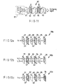
- FIG 11 illustrates an image operation system 90 which is proposed in the above-mentioned literature.
- the image operation system 90 includes a light source 97 emitting red, blue and green light beams. The light beams are transmitted sequentially through a color polarizing plate 91 , a liquid crystal display device (referred to as the LCD device, hereinafter) 92 , a color polarizing plate 93 , an LCD device 94 , and a color polarizing plate 95 .
- the LCD devices 92 and 94 are, for example, of an active matrix type and perform black and white display.
- the light outgoing from the color polarizing plate 95 indicates the operation result.
- the color polarizing plates 91, 93 and 95 linearly polarize a light beam having a specified wavelength, but transmits a light beam having any other wavelength without such polarization.
- Figures 12a through 12c illustrate a performance of the image operation system 90 .
- the hatched areas are rotation regions which transmit light while rotating the light, and blank areas are transmission regions which transmit light without rotation.
- Figure 12a concerns an image operation system 90a for obtaining an AND ( G1 ⁇ G2 ) of images G1 and G2 displayed in the LCD devices 92 and 94 .
- the color polarizing plates 91, 93 and 95 linearly polarize all the light beams having a wavelength of ⁇ 1 in an identical direction.
- Figure 12b concerns an image operation system 90b for obtaining an OR ( G1 + G2 ) of the images G1 and G2 .
- Light beams having wavelengths of ⁇ 2 and ⁇ 3 are used.
- the color polarizing plate 91 linearly polarizes light beams having a wavelength of ⁇ 2 .
- the color polarizing plate 93 linearly polarizes light beams having wavelengths of ⁇ 2 and ⁇ 3 .
- the color polarizing plate 95 linearly polarizes light beams having a wavelength of ⁇ 3 .
- the light beams having a wavelength of ⁇ 3 are linearly polarized by the color polarizing plate 93 for the first time.
- the light beams linearly polarized by the color polarizing plate 93 only the light beams transmitted through the rectangular transmission region of the LCD device 94 are transmitted through the color polarizing plate 95 , whereby a rectangular image is obtained on the display plane 96 .
- an image made of the circular image G1 and the rectangular image G2 is obtained as the OR operation result on the display plane 96 .
- Figure 12c concerns an image operation system 90c for obtaining an inverted image of an EXCLUSIVE-OR ( G1 EXOR G2 ) of the images G1 and G2 .
- a monochromatic light having a wavelength of ⁇ 4 is used.
- the color polarizing plates 91 and 95 linearly polarize light beams having a wavelength of ⁇ 4 .
- the color polarizing plate 93 which transmits such light beams without polarization, may be eliminated or formed of a transparent glass. In this construction, light beams having a wavelength of ⁇ 4 are linearly polarized by the color polarizing plate 91 .
- the light beams are transmitted through the transmission region of the LCD device 92 without rotation but are rotated at a specified angle by the rotation region of the LCD device 92 .
- the light beams transmitted through the rotation region of the LCD device 94 are further rotated, thereby becoming parallel to the polarizing direction of the color polarizing plate 95 .
- the light beams rotated either by the LCD device 92 or 94 are shielded by the color polarizing plate 95 .
- the light beams transmitted through the transmission region of the LCD device 92 and then the transmission region of the LCD device 94 reach the display plane 96 .
- an inverted image of the XOR of the images G1 and G2 is obtained as the operation result on the display plane 96 .
- the present invention provides a liquid crystal operation device, comprising: first and second substrates opposed to one another: a liquid crystal layer interposed between the substrates; a plurality of first electrodes provided on one of the substrates; an insulating film provided over the first electrodes; a plurality of second electrodes provided on the insulating film, the second electrodes being at least partially opposed to the first electrodes; a third electrode provided on a surface of the other substrate and being opposed to the second electrodes; a plurality of photosensitive sections, each section connecting one of the second electrodes to an associated signal line, each photosensitive section being formed from a photoconductive material; and a black mask provided above the photosensitive sections; wherein the electrodes are arranged so as to provide a first capacitance between the first electrodes and the second electrodes and a second capacitance between the second electrodes and the third electrode, and wherein each second electrode is controllably electrically connected to or insulated from the associated signal line by a respective one of the photosensitive sections.
- the second electrodes and the signal line are separated from each other and arranged in a direction along the surface of one of the substrates, and a portion of a photosensitive section is connected to a respective one of the second electrodes and another portion of the photosensitive section is connected to the signal line associated with the second electrode.
- the device further comprises a plurality of scanning lines, each scanning line being opposed to a respective one of the signal lines with the photosensitive sections being interposed between the scanning line and the signal line, the scanning line being electrically insulated from the second electrodes, the signal line and the photosensitive section.
- the signal line is provided on a portion of the second electrodes with the photosensitive sections being interposed between the signal line and the scanning electrode.
- the present invention also provides an image processing system, comprising: a liquid crystal operation device as defined above; and a spatial light modulator for optically transferring an image to the liquid crystal operation device.
- the spatial light modulator comprises a transparent electrode, a photoconductive layer, a light reflecting layer, a liquid crystal layer and another transparent electrode which are laminated between first and second modulator substrates in this order.
- the image processing system further comprises another liquid crystal operation device which comprises: third and fourth substrates opposed to one another; another liquid crystal layer interposed between the third and fourth substrates; a plurality of fourth electrodes provided on one of the third and fourth substrates; an insulating film provided over the fourth electrodes; and a plurality of fifth electrodes provided on the insulating film, the fifth electrodes being at least partially opposed to the fourth electrodes; a sixth electrode provided on a surface of the other substrate to be opposed to the fifth electrodes; a plurality of photosensitive sections, each photosensitive section connecting one of the fifth electrodes to an associated signal line, each photosensitive section being formed from a photoconductive material; and a black mask provided above the photosensitive sections; wherein the electrodes are arranged so as to provide a third capacitance between the fourth electrodes and the fifth electrodes and a fourth capacitance between the fifth electrodes and sixth electrode; and each fifth electrode is controllably electrically connected to or insulated from the associated signal line by a respective one of the photoconductive sections.
- liquid crystal operation device In a liquid crystal operation device according to the present invention, the following operation is performed as an example.
- a voltage is applied between a signal line and a first electrode, and then a light having an image data is emitted from one of the substrates.
- a charge is accumulated in a capacitance through a photosensitive section in a region exposed to the light.
- the first electrode and a third electrode are shortcircuited, whereby the charge accumulated in the first capacitance is partially transferred to a second capacitance.
- the image data is stored.
- This operation is only an example. Various other operations are possible by other types of processing.
- the invention described herein makes possible the advantages of providing a liquid crystal operation device and an image processing system using the same in which an entire or a partial image operation is directly conducted with no use of an LSI at a high speed with no necessity of positional alignment.
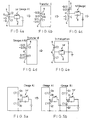
- Figure 1 is a cross sectional view of a liquid crystal operation device according to the present invention.
- Figure 2 is a partial plan view of the liquid crystal operation device of Figure 1 .
- Figure 3 is a view illustrating operations executed by the liquid crystal operation device of Figure 1 .
- FIGS 4a through 4e illustrate equivalent circuits of the liquid crystal operation device of Figure 1 on each step of an AND operation.
- FIGS 5a and 5b illustrate equivalent circuits of the liquid crystal operation device of Figure 1 on each step of an OR operation.
- Figures 6a through 6c illustrate equivalent circuits of the liquid crystal operation device of Figure 1 on each step of an XOR operation.
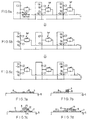
- Figures 7a through 7d illustrate modifications of the liquid crystal operation device of Figure 1 .
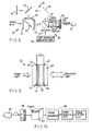
- Figure 8 is a schematic view of an image processing system according to the present invention.
- Figure 9 is a cross sectional view of a spatial light modulator used in the image processing system of Figure 8 .
- Figure 10 is a schematic view of a conventional image processing system.
- Figure 11 is a schematic view of another conventional image processing system.
- Figures 12a through 12c are views illustrating operations performed by the conventional image processing system of Figure 11 .
- FIG. 1 illustrates a liquid crystal operation device according to the present invention.
- the liquid crystal operation device includes a pair of opposed glass substrates 1 and 2 and a liquid crystal 3 enclosed therebetween.
- a plurality of lower electrodes 4 formed of Al or the like are provided, and an insulating film 5 is provided on the glass substrate 1 to cover the lower electrodes 4 .
- a plurality of pixel electrodes 6 are provided to be opposed to the lower electrodes 4 .
- the lower electrodes 4 are arranged in stripes in a great number (only three are shown in Figure 2 ), and the pixel electrodes 6 are arranged in a matrix in a great number (nine in Figure 2 ).
- An auxiliary capacitance C1 is generated between each pixel electrode 6 and the corresponding lower electrode 4 .
- Source lines 7 as signal lines are disposed between the lower electrodes 4 and extended in parallel with the lower electrodes 4 .
- the pixel electrodes 6 provided on an identical lower electrode 4 are electrically connected to an identical source line 7 each through a photosensitive section 8 formed of a photoconductive material having a resistance changed by light irradiation.
- the source lines 7 are provided for supplying the pixel electrodes 6 with an image signal.
- Each photosensitive section 8 is covered with a black mask 10 , which is provided for preventing the photosensitive section 8 from being exposed to light for image reading which is emitted, for example, from above.
- the black mask 10 may be provided on the side of the other glass substrate 2 (upper one in Figure 1 ).
- a counter electrode 9 is provided on a substantially entire surface of the glass substrate 2 , the surface being opposed to the glass substrate 1 .
- the counter electrode 9 is opposed to all the pixel electrodes 6 with the liquid crystal 3 therebetween.
- a liquid crystal capacitance C2 is generated between the counter electrode 9 and each pixel electrode 6 , utilizing the dielectric characteristic of the liquid crystal 3 .
- the counter electrode 9 can be electrically connected to all the lower electrodes 4 through a specified shortcircuiting device (not shown).
- the liquid crystal operation device having the above-mentioned construction was produced in the following manner.
- an Al film was formed in a thickness of 150 nm by use of electron beam evaporation on the lower glass substrate 1 and then etched to obtain the lower electrodes 4 in stripes each having a width of 50 ⁇ m.
- an Al 2 O 3 film and a SiN x film were sequentially formed by use of sputtering to obtain the insulating film 5 in a total thickness of 300 nm.
- the pixel electrodes 6 are arranged in a matrix of 120 pcs. (longitudinal) x 160 pcs. (transverse). Each pixel electrode 6 has a size of 300 ⁇ m x 300 ⁇ m. The arranging pitch of the pixel electrodes 6 is 500 ⁇ m, and the gap between the adjacent pixel electrodes 6 is 50 ⁇ m.
- an a-Si (amorphous silicon) film was formed in a thickness of 200 nm by use of plasma CVD and then etched to obtain the photosensitive sections 8 . Then, the black masks 10 were formed of a black pigment to cover the photosensitive sections 8 .
- ITO On a substantially entire surface of the upper glass substrate 2 , ITO was deposited to form the counter electrode 9 .
- SiO 2 was deposited in a thickness of 30 nm by use of sputtering, thereafter a polyimide film for horizontal alignment was coated thereon by a spinner, and the resultant surfaces were rubbed so that the liquid crystal 3 to be enclosed would be twisted at 90°.
- the glass substrates 1 and 2 were bonded together with plastic beads having a diameter 6 ⁇ m therebetween, and then the liquid crystal 3 (for example, ZLI-1565 produced by E. Merck) was enclosed, thereby producing a liquid crystal panel. Then, the liquid crystal panel was interposed between a pair of polarizing plates, thereby producing a liquid crystal operation device.
- the liquid crystal 3 a liquid crystal which had been purified to have a resistance of 1 x 10 11 ⁇ cm or higher was used.
- All the source lines 7 and all the lower electrodes 4 are applied with a voltage.
- light from an image to be operated for example, an image A
- a desired charge is accumulated in an auxiliary capacitance C1 only through the photosensitive section 8 in a region exposed to the light.
- the resistance of the liquid crystal 3 should be sufficiently high to enhance the charge holding capability of the liquid crystal 3 and thus to prevent the charges from being lost in a short period of time, so that two charges can be added.
- the liquid crystal having the above-mentioned resistance of 1 x 10 11 ⁇ cm was used.
- This operation is an example, but other operations can be performed by other processes according to the present invention.
- a rectangular mask extended in the transverse direction and another rectangular mask extended in the longitudinal direction are exposed to parallel light.
- the light emitted to the former mask is identified as an operation light for the image A
- the light emitted to the latter mask is identified as an operation light for the image B .
- the operations are performed by sequentially emitting these operation lights from below the liquid crystal operation device, and then emitting light for reading from above.
- the light for reading is obtained from a light generating device including, for example, a semiconductor laser emitting visible light and a lens.
- All the source lines 7 and all the lower electrodes 4 are applied with a voltage, and the operation light for the image A ((1) in Figure 3 ) is emitted from below the liquid crystal operation device.
- a desired charge is accumulated in the auxiliary capacitance C1 only through the photosensitive section 8 in a region exposed to the light.
- the lower electrode 4 and the pixel electrode 6 generating the auxiliary capacitance C1 have potentials of -Q and +Q, respectively.
- All the source lines 7 and all the lower electrodes 4 are applied with a voltage of the same polarity as that of the voltage previously applied, and the operation light for the image B ((2) in Figure 3 ) is emitted from below the liquid crystal operation device.
- a desired charge is accumulated in the auxiliary capacitance C1 only through the photosensitive section 8 in a region exposed to the light.
- the liquid crystal capacitance C2 does not change, but the potentials of the lower electrode 4 and the pixel electrode 6 generating the auxiliary capacitance C1 are changed to -Q and +Q, respectively.
- the liquid crystal 3 Since the liquid crystal 3 has a sufficiently high resistance as mentioned before, the charges are not lost in a short period of time. If the threshold voltage for realignment of liquid crystal molecules is set between the level at Transfer I and the level at Transfer II , the liquid crystal molecules are realigned by the charge transferred in Transfer II only in a portion of the liquid crystal 3 where the images A and B overlap. As a result, that portion is optically modulated to execute an AND operation of the images A and B . The operation result is indicated by hatching in (3) of Figure 3 .
- the light for reading is emitted to read out the operation result.
- the threshold voltage for realignment of the liquid crystal molecules is set equal to or higher than the level at Transfer II , only a portion of the liquid crystal 3 where three or more images overlap is optically modulated to execute an AND operation of the three images.
- the liquid crystal operation device can be initialized by grounding the source lines 7 , the lower electrodes 4 and the counter electrode 9 , and then emitting light to the liquid crystal operation device.
- an equivalent circuit at this point Figure 4e
- no charge is accumulated in the auxiliary capacitance C1 or in the liquid crystal capacitance C2 .
- the source lines 7 and the counter electrode 9 are applied with a voltage.
- the lower electrodes 4 and the counter electrode 9 may be shortcircuited to have an identical potential with each other so that the auxiliary capacitance C1 will also be used.
- a voltage equal to or higher than the threshold voltage for realignment of liquid crystal molecules is applied to the source lines 7 and the counter electrode 9 , and the operation light for the image A is emitted from below in this state.
- the operation light for the image A is emitted from below in this state.
- Only a portion of the liquid crystal 3 corresponding to the pixel electrode 6 exposed to the light is applied with a high voltage, and thus optically modulated.
- An equivalent circuit at this point is shown in Figure 5a .
- the realignment state of the liquid crystal 3 is stored by the charge holding capability of the liquid crystal 3 or of the auxiliary capacitance C1 . In other words, the image A is kept in the liquid crystal 3 .
- An OR image operation can be executed throughout the charge holding time.
- For writing the image B it is acceptable to use a voltage having an opposite polarity from the voltage used for the image A as long as the voltage is sufficiently high to drive the liquid crystal 3 .
- the method for initialization and the effect of the voltage polarity on a subsequent operation are identical with those in the case of the AND operation.
- the source lines 7 and the counter electrode 9 are applied with a voltage.
- the lower electrodes 4 and the counter electrode 9 may be shortcircuited to have an identical potential with each other so that the auxiliary capacitance C1 will also be used.
- a voltage equal to or higher than the threshold voltage for realignment of the liquid crystal molecules is applied to the source lines 7 and the counter electrode 9 , and the operation light for the image A is emitted from below in this state.
- the operation light for the image A is emitted from below in this state.
- only a portion of the liquid crystal 3 corresponding to the pixel electrode 6 exposed to the light is applied with a high voltage, and thus optically modulated.
- An equivalent circuit at this point is shown in Figure 6a . Even after the light is removed, the realignment state of the liquid crystal 3 is stored by the charge holding capability of the liquid crystal 3 or of the auxiliary capacitance C1 .
- the source lines 7 and the counter electrode 9 are applied with a voltage having an opposite polarity from the voltage previously applied, and the operation light for the image B is emitted from below.
- An equivalent circuit at this point is shown in Figure 6b .
- the emission of the operation light for the image B the charge accumulated by the operation light for the image A is discharged down to a value equal to or lower than that of the threshold voltage for realignment of the liquid crystal molecules. Therefore, a portion of the liquid crystal 3 corresponding to the pixel electrode 6 exposed both to the operation light for the image A and the operation light for the image B , namely, to the pixel electrode 6 where the charge is discharged is initialized.
- Another portion of the liquid crystal 3 corresponding to the pixel electrode 6 exposed only to the operation light for the image B is applied with a voltage which has an opposite polarity from the voltage previously applied but has a value equal to or higher than that of the threshold voltage for realignment of the liquid crystal molecules, and thus is optically modulated. Still another portion of the liquid crystal 3 corresponding to the pixel electrode 6 exposed to the operation light for the image A but not to the operation light for the image B keeps the realignment state by the aforementioned charge holding capability.
- An equivalent circuit at this point is shown in Figure 6c .
- the AND, OR and XOR operations can be executed in one operation device with no necessity of any positional alignment which is conventionally required.
- a material of the photosensitive section 8 other materials than a-Si can be used.
- Usable materials include amorphous silicons such as a-SiC and a-SiN, inorganic materials including amorphous chalcogenide such as a-Se, a-Se ⁇ Te, a-Se ⁇ As and a-As 2 Se 3 , inorganic crystals such as ZnO, CdS and BSO(Bi 12 SiO 20 )BGO(Bi 12 GeO 20 ), and organic photoconductive materials such as polyvinyl carbazole and a bisazo pigment.
- the insulating film 5 may have a one-layer structure or a three-layer structure instead of a two-layer structure.
- an inorganic material such as SiO 2 or Ta 2 O 5
- an organic material such as polyimide, polyvinyl alcohol or polyamide may be used instead of Al 2 O 3 and SiN x .
- the pixel electrodes 6 and the counter electrode 9 may be formed of SnO 2 or the like instead of ITO.
- the source lines 7 and the lower electrodes 4 may be formed of Al, Cr, Ta, Mo, Ti or other metal materials instead of ITO.
- the black masks 10 may be formed of an organic material containing a black pigment or a black dye or a color inorganic material instead of a black pigment. In the case when the black masks 10 are formed at positions which are not influenced by the shortcircuit between the lower electrodes 4 and the counter electrode 9 , for example, on a surface of the counter electrode 9 , the black masks 10 may be formed of a metal.
- liquid crystal 3 a nematic, smectic, or chiral nematic liquid crystal may be used.
- a display mode a TN, STN, phase transition, ECB, guest-host, or ferroelectric mode may be used. It is desirable to use a liquid crystal having a high resistance for enhancing the charge holding capability.
- the construction in the vicinity of the photosensitive section 8 is not limited to the one shown in Figure 1 , but may be as shown in Figures 7a, 7b, 7c or 7d .
- Figure 7a an end portion of the pixel electrode 6 and a side peripheral portion of the source line 7 are disposed on the photosensitive section 8 .
- a lamination having the photosensitive section 8 and a gate line 11 as a scanning line with a gate insulating film 12 interposed therebetween is inserted from between an end portion of the pixel electrode 6 and the insulating film 5 to between a side peripheral portion of the source line 7 and the insulating film 5 .
- another insulating film as an etching stop layer 13 is inserted from between the photosensitive section 8 and the end portion of the pixel electrode 6 to between the photosensitive section 8 and the side peripheral portion of the source line 7 .
- this is the construction of a reverse stagger TFT.
- the source line 7 in Figure 7b and the gate line 11 in Figures 7c and 7d may be formed of a metal, in which case, the source line 7 and the gate line 11 each act as a light shielding member in addition to being a conductive member.
- Usable metals include Al, Cr, Ta, Mo and Ti.
- a Cr film was formed on a glass substrate (not shown) in a thickness of 150 nm by use of sputtering and then etched to obtain lower electrodes (not shown) each having a width of 50 ⁇ m.
- an SiN x film was formed in a thickness of 200 nm by use of plasma CVD to obtain the insulating film 5 .
- a Ta film was formed in a thickness of 150 nm by use of sputtering, and then etched to obtain the gate line 11 .
- An upper surface of the gate line 11 was anodized into a Ta 2 O 5 layer.
- an SiN x layer (referred to as the lower SiN x layer), an a-Si layer and another SiN x layer (referred to as the upper SiN x layer) were sequentially laminated by use of plasma CVD.
- a total thickness of the Ta 2 O 5 layer and the lower SiN x layer is approximately 150 nm.
- the a-Si layer has a thickness of approximately 250 nm, and the upper SiN x layer has a thickness of approximately 100 nm.
- the upper SiN x layer and the a-Si layer were treated with dry etching to be the etching stop layer 13 and the photosensitive section 8 (semiconductor layer), respectively.
- a-Si(n + ) film was formed in a thickness of 30 nm by use of plasma CVD, and then an ITO film was formed in a thickness of 150 nm by use of sputtering. These layers were etched to obtain a contact layer (not shown) of a-Si(n + ), the source line 7 acting as a source electrode and the pixel electrode 6 both of ITO.
- an ITO film was formed on an entire surface of another glass substrate to obtain a counter electrode.
- the gate line 11 also acts as a black mask, the light for operation is emitted from the side of the etching stop layer 13 and the light for reading is emitted from the side of the gate line 11 .
- the gate line 11 was floated, and an operation of diagrams was executed in the same way as in the preceding example, to confirm the liquid crystal operation device was capable of AND, OR and XOR operations.
- a signal indicating a circle was inputted to the pixel electrode 6 from the source line 7 using the gate line 11 .
- the gate line 11 was floated again, and an optical signal indicating a rectangle or the like was inputted.
- the value and the polarity of the voltage applied between the source line 7 and the counter electrode, and between the source line 7 and the lower electrode were changed based on the above-mentioned operation principle, to confirm that the AND, OR and XOR operations were executed.
- the lower electrode 4 need not have the same width as that of the pixel electrode 6 as is in Figure 1 .
- the lower electrode 4 when being exposed to light a plurality of times, supplies charges for driving the liquid crystal 3 . Accordingly, the width of the lower electrode 4 is determined in accordance with an area thereof, which is based on the threshold voltage, capacity and resistance of the liquid crystal 3 , dielectric constant and thickness of the insulating film, and the like.
- a source signal running through the source line 7 can be sent to the pixel electrode 6 by a gate signal running through the gate line 11 . Accordingly, an operation can be executed based on the above-mentioned principle by electrically forming an image A by a known TFT driving method and then optically writing an image B on the image A . In other words, an operation of a fixed pattern and a variable pattern can be executed. For example, in a mask inspection or an inspection of component mounting, an original image is inputted as a fixed pattern to the liquid crystal operation device by a TFT driving method, and then an image for inspection carried on an inspection line is optically inputted as a variable pattern to the liquid crystal operation device.
- the voltage applying conditions such as the value, polarity and length of time are adjusted to match a desired operation based on the above-mentioned principle.
- defects can be detected in a short period of time by an XOR operation.
- the parameters which determine the photoconductive characteristics of the semiconductor material used in the liquid crystal operation device should be much better than those of a semiconductor material used in a usual LCD device having a TFT structure.
- an a-Si layer should have a thickness of 50 nm or more.
- FIG. 8 illustrates an image processing system according to the present invention, to which the liquid crystal operation device is applied.
- the image processing system includes a liquid crystal operation device 30 , a laser source 31 for emitting a laser beam for reading an image displayed in the liquid crystal operation device 30 , a beam splitter 32 for supplying the liquid crystal operation device 30 with two types of light given from two directions, an operation light emitter 25 provided under the beam splitter 32 for emitting one of the types of light, namely, operation light, an image light emitter 20 provided to the left (in Figure 8 ) of the beam splitter 32 for emitting the other type of light, namely, image light, and a monitor 33 for transferring the image based on light emitted from an upper side of the beam splitter 32 .
- the operation light emitter 25 includes a light source 26 for emitting the operation light and a liquid crystal shutter 27 for transmitting or shielding the light emitted by the light source 26 .
- the light emitted by the light source 26 is sent to the liquid crystal operation device 30 through the beam splitter 32 at a specified timing.
- the monitor 33 includes a mirror 34 for reflecting the light emitted from the upper side of the beam splitter 32 , a half mirror 35 for receiving the light reflected by the mirror 34 , and a screen 36 for receiving the light transmitted through the half mirror 35 .
- a mirror 34 for reflecting the light emitted from the upper side of the beam splitter 32
- a half mirror 35 for receiving the light reflected by the mirror 34
- a screen 36 for receiving the light transmitted through the half mirror 35 .
- an image monitored is displayed on the screen 36 .
- the light reflected by the half mirror 35 is sent to another liquid crystal shutter 24 (described later).
- the image light emitter 20 includes still another liquid crystal shutter 21 , a spatial light modulator (referred to as SLM, hereinafter) 23 for receiving an image data through the liquid crystal shutter 21 , another half mirror 22 provided between the SLM 23 and the liquid crystal shutter 21 , and the liquid crystal shutter 24 provided above the half mirror 22 .
- SLM spatial light modulator
- the SLM 23 includes a pair of glass substrates 41 and 48 , a transparent electrode 42, a photoconductive layer 43 , a light shielding layer 44 , a light reflecting layer 45 , a liquid crystal layer 46 , and another transparent electrode 47 .
- the above electrodes and layers are formed in the above-mentioned order from the side of the glass substrate 41 .
- a voltage is applied to the liquid crystal layer 46 through the photoconductive layer 43, the light shielding layer 44 , and the light reflecting layer 45 . Then, image light, namely, light from a fixed image as a fixed image data is emitted from the side of the glass substrate 41 . Since the resistance of a portion of the photoconductive layer 43 exposed to the image light is lowered, a high voltage is applied to a portion of the liquid crystal layer 46 corresponding to the above portion of the photoconductive layer 43 , whereby the alignment of the liquid crystal molecules in the above portion are changed. Operation light from the light source 26 is incident on the side of the glass substrate 48 through the beam splitter 32 .
- the operation light is reflected by the light reflecting layer 45 but is modulated at the portion of the liquid crystal layer 46 where the alignment is changed.
- the image light which is incident on the side of the glass substrate 41 can be taken out-as reflected image light by the operation light incident from the side of the glass substrate 48 .
- the reflected image light can be used as an image data for an operation.
- operations are practically executed in the following manner.
- a data concerning a fixed image A in the form of light is inputted to the SLM 23 through the liquid crystal shutter 21 , whereby the SLM 23 forms a reflected image of the image data as mentioned above.
- Operation light is emitted to the beam splitter 32 through the liquid crystal shutter 27 for a desired period of time and is projected on the SLM 23 having the reflected image, and then is written into the liquid crystal operation device 30 through the beam splitter 32 .
- a data of an image B for operation is written into the liquid crystal operation device 30 in the same manner. In this way, an operation is executed.
- the image data displayed in the liquid crystal operation device 30 as the operation result is displayed on the screen 36 through the beam splitter 32 , the mirror 34 and the half mirror 35 , and also is transferred to the incident side of the SLM 23 .
- the operation result is confirmed based on the image displayed on the screen 36 .
- a subsequent operation is executed based on the new data and the preceding image data which has been transferred to the incident side of the SLM 23 .
- liquid crystal shutters 21 , 24 and 27 a surface stabilized ferroelectric liquid crystal (SSF-LC) using CS-14 (described in detail later) were used. Instead of the liquid crystal shutters, other types of shutters may be used. It is desirable to use high speed shutters in order to execute high speed operations.
- SSF-LC surface stabilized ferroelectric liquid crystal
- an optical processing system such as a CCD or an image processing LSI is used for electrically processing image data.
- Other optical systems may be used.
- the image processing system according to the present invention is not limited to the one shown in Figure 8 , but may have any construction including the liquid crystal operation device and an SLM as long as an operation is executed based on an image data obtained by the liquid crystal operation device and sent to the SLM and another image data inputted to the liquid crystal operation device from another system.
- the SLM 23 was produced in the following manner.
- the transparent electrodes 42 and 47 were formed by depositing ITO in a thickness of 150 nm each by use of sputtering.
- the photoconductive layer 43 was formed by depositing a-Si in a thickness of approximately 1 ⁇ m by use of plasma CVD.
- the light shielding layer 44 was formed by coating the photoconductive layer 43 with polyimide containing a black pigment by a spinner and then heating the polyimide.
- the light reflecting layer 45 was formed by laminating TiO 2 films and SiO 2 films in a total approximate number of 20.
- the liquid crystal layer 46 was formed of, for example, CS-14, which is a ferroelectric liquid crystal produced by Chisso Petrochemical Corp.
- the liquid crystal layer 46 has a thickness of approximately 2 ⁇ m.
- the liquid crystal molecules were aligned by an alignment film formed of nylon.
- the image inputted to the SLM 23 can be converted into a binary code.
- a positive or a negative image of the inputted image can be obtained.
- the photosensitivity of the SLM 23 is 80 ⁇ W/cm 2 , and the applied voltage is ⁇ 30 V at the maximum.
- the ferroelectric mode display mode using the ferroelectric liquid crystal
- a memory image of the inputted image can be obtained.
- HFE mode TN mode having a twist angle of approximately 45°
- a negative image or a positive image can easily be formed only by rotating the polarizing plate by 90°.
- a negative image or a positive image can be obtained only by reversing the polarity of the applied voltage.
- an enlarged image or a reduced image can be obtained by changing the value of the voltage or the frequency.
- the SLM 23 enables processing of an image to obtain an enlarged, reduced, rotated, moved, negative/positive-converted or binary image.
- the image processing system may include a combination of the liquid crystal operation device shown in Figure 1 and the one shown in Figure 7c or 7d . Since a plurality of different image data can be processed by the liquid crystal operation device having a TFT structure as described above, three images can be subjected to AND, OR and XOR operations, outline extraction (XOR of an image and an enlarged image thereof) and enlargement.
- image outline extraction, image comparison (XOR or AND of an image and another image), image enlargement (OR of an image and an enlarged image thereof), formation of a binary image (by use of an SLM), and other general image processing can be performed at a high speed. Therefore, the image processing system is applicable to a wide range of industrial and consumer uses including various inspections using images (process inspection, mask inspection, etc.), acceleration sensors (used for preventing vibration while being handled by a hand, and for controlling standing tilt of vehicles, etc.), extraction of moving objects, voice recognition, fingerprint collation, and character recognition.
- an operation is executed by emitting two or more types of operation light to at least one liquid crystal operation device at different times. Therefore, positional alignment is not necessary. Moreover, since the operation is executed by two or more light emissions, high speed processing effective for dealing with a large amount of data is realized.
Landscapes
- Physics & Mathematics (AREA)
- Nonlinear Science (AREA)
- General Physics & Mathematics (AREA)
- Mathematical Physics (AREA)
- Chemical & Material Sciences (AREA)
- Crystallography & Structural Chemistry (AREA)
- Optics & Photonics (AREA)
- Liquid Crystal (AREA)
- Engineering & Computer Science (AREA)
- Theoretical Computer Science (AREA)
Claims (7)
- Flüssigkristall-Funktionsvorrichtung mit:einem ersten und einem zweiten Substrat (1, 2), die einander gegenüberstehen;einer Flüssigkristallschicht (3), die zwischen die Substrate eingefügt ist;einer Vielzahl erster Elektroden (4), die auf einem der Substrate (1) vorhanden sind;einem Isolierfilm (5), der auf den ersten Elektroden (4) vorhanden ist;einer Vielzahl zweiter Elektroden (6), die auf dem Isolierfilm vorhanden sind, wobei diese zweiten Elektroden (6) zumindest teilweise den ersten Elektroden gegenüberstehen;einer dritten Elektrode (9), die auf einer Oberfläche des anderen Substrats (2) vorhanden ist und den zweiten Elektroden (6) gegenübersteht;einer Vielzahl photoempfindlicher Abschnitte (8), wobei jeder Abschnitt eine der zweiten Elektroden (6) mit einer zugeordneten Signalleitung verbindet, wobei jeder photoempfindliche Abschnitt aus einem photoleitenden Material besteht;und einer Schwarzmaske (10), die über den photoempfindlichen Abschnitten (8) vorhanden ist;wobei die Elektroden so angeordnet sind, dass sie eine erste Kapazität (C1) zwischen den ersten Elektroden (4) und den zweiten Elektroden (6) sowie eine zweite Kapazität (C2) zwischen den zweiten Elektroden (6) und der dritten Elektrode (9) bilden, und wobei jede zweite Elektrode (6) über einen jeweiligen der photoempfindlichen Bereiche kontrollierbar elektrisch mit der zugeordneten Signalleitung verbunden oder gegen diese isoliert ist.
- Flüssigkristall-Funktionsvorrichtung nach Anspruch 1, bei der die zweiten Elektroden (6) und die Signalleitungen (7) voneinander getrennt sind und sie in einer Richtung entlang der Oberfläche eines der Substrate angeordnet sind, und ein Teil eines photoempfindlichen Abschnitts (8) mit einer jeweiligen der zweiten Elektroden verbunden ist, während ein anderer Teil des photoempfindlichen Abschnitts mit der Signalleitung (7) verbunden ist, die der zweiten Elektrode zugeordnet ist.
- Flüssigkristall-Funktionsvorrichtung nach Anspruch 2, ferner mit einer Vielzahl von Abrasterleitungen (11), von denen jede einer jeweiligen der Signalleitungen (7) gegenübersteht, wobei die photoempfindlichen Abschnitte zwischen die Abrasterleitung und die Signalleitung (7) eingefügt sind, wobei die Abrasterleitung elektrisch gegen die zweiten Elektroden (6), die Signalleitung (7) und die photoempfindlichen Abschnitte (8) isoliert ist.
- Flüssigkristall-Funktionsvorrichtung nach Anspruch 1, bei der die Signalleitung auf einem Teil der zweiten Elektroden (6) vorhanden ist, wobei die photoempfindlichen Abschnitte zwischen die Signalleitung und die Abrasterelektrode eingefügt sind.
- Bildverarbeitungssystem mit:einer Flüssigkristall-Funktionsvorrichtung, wie sie in einem der vorstehenden Ansprüche definiert ist; undeinem Raumlichtmodulator (23) zum optischen Übertragen eines Bilds an die Flüssigkristall-Funktionsvorrichtung.
- Bildverarbeitungssystem nach Anspruch 5, bei dem der Raumlichtmodulator eine transparente Elektrode (42), eine photoleitende Schicht (43), eine Lichtreflexionsschicht (45), eine Flüssigkristallschicht (46) und eine andere transparente Elektrode (47) aufweist, die in dieser Reihenfolge zwischen ein erstes und ein zweites Modulatorsubstrat (41, 42) laminiert sind.
- Bildverarbeitungssystem nach Anspruch 5 oder 6, ferner mit einer anderen Flüssigkristall-Funktionsvorrichtung, die folgendes aufweist:ein drittes und ein viertes Substrat, die einander gegenüberstehen;eine weitere Flüssigkristallschicht, die zwischen das dritte und vierte Substrat eingefügt ist;eine Vielzahl vierter Elektroden, die auf dem dritten oder vierten Substrat vorhanden sind;einen Isolierfilm, der auf den vierten Elektroden vorhanden ist;eine Vielzahl fünfter Elektroden, die auf dem Isolierfilm vorhanden sind und zumindest teilweise den vierten Elektroden gegenüberstehen;eine sechste Elektrode, die auf einer Oberfläche des anderen Substrats vorhanden ist, um den fünften Elektroden gegenüberzustehen;eine Vielzahl photoempfindlicher Abschnitte, von denen jeder eine der fünften Elektroden mit einer zugeordnet Signalleitung verbindet, wobei jeder photoempfindliche Abschnitt aus einem photoleitenden Material besteht; undeiner Schwarzmaske, die über den photoempfindlichen Abschnitten vorhanden ist;wobei die Elektroden so angeordnet sind, dass sie zwischen den vierten Elektroden und den fünften Elektroden eine dritte Kapazität sowie zwischen den fünften Elektroden und den sechsten Elektroden eine vierte Kapazität bilden;und wobei jede fünfte Elektrode über einen jeweiligen der photoleitenden Abschnitte kontrollierbar elektrisch mit der zugehörigen Signalleitung verbunden oder gegen diese isoliert ist.
Applications Claiming Priority (2)
| Application Number | Priority Date | Filing Date | Title |
|---|---|---|---|
| JP3286740A JP2738613B2 (ja) | 1991-10-31 | 1991-10-31 | 液晶演算素子及びこれを用いた画像処理システム |
| JP286740/91 | 1991-10-31 |
Publications (3)
| Publication Number | Publication Date |
|---|---|
| EP0540367A2 EP0540367A2 (de) | 1993-05-05 |
| EP0540367A3 EP0540367A3 (en) | 1993-05-19 |
| EP0540367B1 true EP0540367B1 (de) | 1998-01-21 |
Family
ID=17708417
Family Applications (1)
| Application Number | Title | Priority Date | Filing Date |
|---|---|---|---|
| EP92310004A Expired - Lifetime EP0540367B1 (de) | 1991-10-31 | 1992-11-02 | Flüssigkristall-Rechnergerät und darauf basierendes Bildverarbeitungssystem |
Country Status (5)
| Country | Link |
|---|---|
| US (1) | US5321536A (de) |
| EP (1) | EP0540367B1 (de) |
| JP (1) | JP2738613B2 (de) |
| KR (1) | KR960012668B1 (de) |
| DE (1) | DE69224144T2 (de) |
Families Citing this family (14)
| Publication number | Priority date | Publication date | Assignee | Title |
|---|---|---|---|---|
| JP3012421B2 (ja) * | 1993-02-08 | 2000-02-21 | シャープ株式会社 | 反射型液晶表示装置 |
| JP3085633B2 (ja) * | 1994-11-08 | 2000-09-11 | シャープ株式会社 | 反射型液晶表示装置 |
| JP3423232B2 (ja) * | 1998-11-30 | 2003-07-07 | 三洋電機株式会社 | アクティブ型el表示装置 |
| JP2000310774A (ja) * | 1999-04-28 | 2000-11-07 | Asahi Glass Co Ltd | カラー液晶表示装置 |
| JP2003107438A (ja) * | 2000-09-12 | 2003-04-09 | Canon Inc | 液晶素子 |
| ITRM20010124A1 (it) * | 2001-03-12 | 2002-09-12 | Univ Roma | Pannello di visualizzazione a cristalli liquidi. |
| US6819469B1 (en) * | 2003-05-05 | 2004-11-16 | Igor M. Koba | High-resolution spatial light modulator for 3-dimensional holographic display |
| US20050094855A1 (en) * | 2003-10-29 | 2005-05-05 | Proano Cesar H. | Fingerprint imaging using a flat panel detector |
| KR100972502B1 (ko) * | 2003-12-30 | 2010-07-26 | 엘지디스플레이 주식회사 | 액정표시장치의 등급표시 자동화 장치 및 이의 동작 방법 |
| US7132667B2 (en) * | 2004-02-11 | 2006-11-07 | General Electric Company | Method and apparatus for improved data acquisition using a solid state digital X-ray detector |
| JP4744914B2 (ja) * | 2005-04-01 | 2011-08-10 | 三菱電機株式会社 | 液晶表示装置及びこれを用いた大型液晶表示装置 |
| US7382512B2 (en) * | 2005-10-26 | 2008-06-03 | Zhizhang Chen | Resistivity phase change material |
| CN101609855B (zh) * | 2008-06-20 | 2013-09-18 | 群康科技(深圳)有限公司 | 光敏电容、光感测电路、基板及其制造工艺和显示装置 |
| KR102856175B1 (ko) * | 2020-06-19 | 2025-09-05 | 주식회사 원익아이피에스 | 비정질 실리콘 박막 형성방법, 그를 포함하는 반도체 소자제조방법 및 그에 의하여 제조된 반도체 소자 |
Family Cites Families (3)
| Publication number | Priority date | Publication date | Assignee | Title |
|---|---|---|---|---|
| US4114991A (en) * | 1976-12-22 | 1978-09-19 | Hughes Aircraft Company | Visible-to-infrared converter light valve |
| US5042917A (en) * | 1986-04-25 | 1991-08-27 | Matsushita Electric Industrial Co., Ltd. | Liquid crystal matrix display unit |
| JPH02143778A (ja) * | 1988-11-25 | 1990-06-01 | Victor Co Of Japan Ltd | 電荷潜像の読取り方式 |
-
1991
- 1991-10-31 JP JP3286740A patent/JP2738613B2/ja not_active Expired - Lifetime
-
1992
- 1992-10-30 US US07/969,104 patent/US5321536A/en not_active Expired - Lifetime
- 1992-10-31 KR KR1019920020460A patent/KR960012668B1/ko not_active Expired - Lifetime
- 1992-11-02 EP EP92310004A patent/EP0540367B1/de not_active Expired - Lifetime
- 1992-11-02 DE DE69224144T patent/DE69224144T2/de not_active Expired - Lifetime
Also Published As
| Publication number | Publication date |
|---|---|
| US5321536A (en) | 1994-06-14 |
| KR960012668B1 (ko) | 1996-09-23 |
| JP2738613B2 (ja) | 1998-04-08 |
| DE69224144D1 (de) | 1998-02-26 |
| EP0540367A3 (en) | 1993-05-19 |
| EP0540367A2 (de) | 1993-05-05 |
| DE69224144T2 (de) | 1998-08-06 |
| KR930008662A (ko) | 1993-05-21 |
| JPH05273511A (ja) | 1993-10-22 |
Similar Documents
| Publication | Publication Date | Title |
|---|---|---|
| EP0540367B1 (de) | Flüssigkristall-Rechnergerät und darauf basierendes Bildverarbeitungssystem | |
| KR100403932B1 (ko) | 액티브 매트릭스 기판, 그 제조방법 및 그 기판을 이용한 이미지 센서 | |
| US5646432A (en) | Semiconductor thin film formed on a supporting substrate | |
| US6977701B2 (en) | Transflective liquid crystal device and electronic apparatus using the same | |
| US6122027A (en) | Liquid crystal display device with color filters between reflector and transparent conductor | |
| JPH05323295A (ja) | 液晶素子およびそれを用いた電子装置 | |
| CN1877401A (zh) | 具有图像感应功能的液晶显示器件 | |
| KR100731045B1 (ko) | 횡전계 방식의 액정표시장치 및 그 제조방법 | |
| US7088415B2 (en) | Electro-optic panel and manufacturing method thereof | |
| US4884875A (en) | Liquid crystal light valve showing an improved display contrast | |
| JP3102834B2 (ja) | 集積型電気光学液晶装置およびその装置を用いる方法 | |
| US20100041174A1 (en) | Liquid crystal display panel and method for manufacturing the same | |
| KR100514507B1 (ko) | 전기 광학 장치 및 그 제조 방법 | |
| US20100283923A1 (en) | Liquid crystal device and electronic apparatus | |
| US7042542B2 (en) | In-plane switching mode liquid crystal display device and method for manufacturing the same | |
| JP4154880B2 (ja) | 電気光学装置及びその製造方法 | |
| JPH0289029A (ja) | 記憶装置および液晶表示装置 | |
| JP3071650B2 (ja) | 液晶表示装置の製造方法 | |
| JPS6328308B2 (de) | ||
| KR20050037846A (ko) | 수평전계방식 액정표시소자 및 그 제조방법 | |
| JP2763223B2 (ja) | 液晶ライトバルブ | |
| JPWO2018198710A1 (ja) | 液晶表示パネルおよび電子機器 | |
| JPH0318829A (ja) | 空間光変調素子 | |
| JPH0650808A (ja) | フタロシアニン光導電層を有する撮像素子および該撮像素子を用いた撮像装置 | |
| JPH075489A (ja) | 画像処理装置及び画像処理方法 |
Legal Events
| Date | Code | Title | Description |
|---|---|---|---|
| PUAI | Public reference made under article 153(3) epc to a published international application that has entered the european phase |
Free format text: ORIGINAL CODE: 0009012 |
|
| PUAL | Search report despatched |
Free format text: ORIGINAL CODE: 0009013 |
|
| AK | Designated contracting states |
Kind code of ref document: A2 Designated state(s): DE FR GB NL |
|
| AK | Designated contracting states |
Kind code of ref document: A3 Designated state(s): DE FR GB NL |
|
| 17P | Request for examination filed |
Effective date: 19930813 |
|
| 17Q | First examination report despatched |
Effective date: 19960129 |
|
| GRAG | Despatch of communication of intention to grant |
Free format text: ORIGINAL CODE: EPIDOS AGRA |
|
| GRAH | Despatch of communication of intention to grant a patent |
Free format text: ORIGINAL CODE: EPIDOS IGRA |
|
| GRAH | Despatch of communication of intention to grant a patent |
Free format text: ORIGINAL CODE: EPIDOS IGRA |
|
| GRAA | (expected) grant |
Free format text: ORIGINAL CODE: 0009210 |
|
| AK | Designated contracting states |
Kind code of ref document: B1 Designated state(s): DE FR GB NL |
|
| REF | Corresponds to: |
Ref document number: 69224144 Country of ref document: DE Date of ref document: 19980226 |
|
| ET | Fr: translation filed | ||
| PLBE | No opposition filed within time limit |
Free format text: ORIGINAL CODE: 0009261 |
|
| 26N | No opposition filed | ||
| REG | Reference to a national code |
Ref country code: GB Ref legal event code: IF02 |
|
| PGFP | Annual fee paid to national office [announced via postgrant information from national office to epo] |
Ref country code: DE Payment date: 20101027 Year of fee payment: 19 |
|
| PGFP | Annual fee paid to national office [announced via postgrant information from national office to epo] |
Ref country code: GB Payment date: 20101027 Year of fee payment: 19 |
|
| PGFP | Annual fee paid to national office [announced via postgrant information from national office to epo] |
Ref country code: NL Payment date: 20111122 Year of fee payment: 20 Ref country code: FR Payment date: 20111118 Year of fee payment: 20 |
|
| REG | Reference to a national code |
Ref country code: DE Ref legal event code: R071 Ref document number: 69224144 Country of ref document: DE |
|
| REG | Reference to a national code |
Ref country code: DE Ref legal event code: R071 Ref document number: 69224144 Country of ref document: DE |
|
| REG | Reference to a national code |
Ref country code: NL Ref legal event code: V4 Effective date: 20121102 |
|
| REG | Reference to a national code |
Ref country code: GB Ref legal event code: PE20 Expiry date: 20121101 |
|
| PG25 | Lapsed in a contracting state [announced via postgrant information from national office to epo] |
Ref country code: GB Free format text: LAPSE BECAUSE OF EXPIRATION OF PROTECTION Effective date: 20121101 |