EP0540017A1 - MOS gate controlled thyristor - Google Patents
MOS gate controlled thyristor Download PDFInfo
- Publication number
- EP0540017A1 EP0540017A1 EP92118602A EP92118602A EP0540017A1 EP 0540017 A1 EP0540017 A1 EP 0540017A1 EP 92118602 A EP92118602 A EP 92118602A EP 92118602 A EP92118602 A EP 92118602A EP 0540017 A1 EP0540017 A1 EP 0540017A1
- Authority
- EP
- European Patent Office
- Prior art keywords
- region
- semiconductor region
- semiconductor
- gate
- conductivity type
- Prior art date
- Legal status (The legal status is an assumption and is not a legal conclusion. Google has not performed a legal analysis and makes no representation as to the accuracy of the status listed.)
- Granted
Links
- 239000012535 impurity Substances 0.000 claims abstract description 28
- 239000004065 semiconductor Substances 0.000 claims description 206
- 239000000758 substrate Substances 0.000 claims description 52
- 238000009413 insulation Methods 0.000 claims description 3
- 108010075750 P-Type Calcium Channels Proteins 0.000 abstract 1
- 239000010410 layer Substances 0.000 description 36
- 229910052710 silicon Inorganic materials 0.000 description 12
- 239000010703 silicon Substances 0.000 description 12
- XUIMIQQOPSSXEZ-UHFFFAOYSA-N Silicon Chemical compound [Si] XUIMIQQOPSSXEZ-UHFFFAOYSA-N 0.000 description 11
- 238000000034 method Methods 0.000 description 8
- 238000009792 diffusion process Methods 0.000 description 7
- 229910021420 polycrystalline silicon Inorganic materials 0.000 description 5
- 229920005591 polysilicon Polymers 0.000 description 5
- 238000004519 manufacturing process Methods 0.000 description 3
- VYPSYNLAJGMNEJ-UHFFFAOYSA-N Silicium dioxide Chemical compound O=[Si]=O VYPSYNLAJGMNEJ-UHFFFAOYSA-N 0.000 description 2
- 230000003247 decreasing effect Effects 0.000 description 2
- 230000000593 degrading effect Effects 0.000 description 2
- 238000002347 injection Methods 0.000 description 2
- 239000007924 injection Substances 0.000 description 2
- 229910052814 silicon oxide Inorganic materials 0.000 description 2
- 229910001218 Gallium arsenide Inorganic materials 0.000 description 1
- 239000000969 carrier Substances 0.000 description 1
- 230000008021 deposition Effects 0.000 description 1
- 238000010586 diagram Methods 0.000 description 1
- 238000007599 discharging Methods 0.000 description 1
- 239000011229 interlayer Substances 0.000 description 1
- 238000005468 ion implantation Methods 0.000 description 1
- 239000000463 material Substances 0.000 description 1
- 239000011159 matrix material Substances 0.000 description 1
Images


Classifications
-
- H—ELECTRICITY
- H01—ELECTRIC ELEMENTS
- H01L—SEMICONDUCTOR DEVICES NOT COVERED BY CLASS H10
- H01L29/00—Semiconductor devices adapted for rectifying, amplifying, oscillating or switching, or capacitors or resistors with at least one potential-jump barrier or surface barrier, e.g. PN junction depletion layer or carrier concentration layer; Details of semiconductor bodies or of electrodes thereof ; Multistep manufacturing processes therefor
- H01L29/66—Types of semiconductor device ; Multistep manufacturing processes therefor
- H01L29/68—Types of semiconductor device ; Multistep manufacturing processes therefor controllable by only the electric current supplied, or only the electric potential applied, to an electrode which does not carry the current to be rectified, amplified or switched
- H01L29/70—Bipolar devices
- H01L29/74—Thyristor-type devices, e.g. having four-zone regenerative action
- H01L29/749—Thyristor-type devices, e.g. having four-zone regenerative action with turn-on by field effect
-
- H—ELECTRICITY
- H01—ELECTRIC ELEMENTS
- H01L—SEMICONDUCTOR DEVICES NOT COVERED BY CLASS H10
- H01L29/00—Semiconductor devices adapted for rectifying, amplifying, oscillating or switching, or capacitors or resistors with at least one potential-jump barrier or surface barrier, e.g. PN junction depletion layer or carrier concentration layer; Details of semiconductor bodies or of electrodes thereof ; Multistep manufacturing processes therefor
- H01L29/66—Types of semiconductor device ; Multistep manufacturing processes therefor
- H01L29/68—Types of semiconductor device ; Multistep manufacturing processes therefor controllable by only the electric current supplied, or only the electric potential applied, to an electrode which does not carry the current to be rectified, amplified or switched
- H01L29/70—Bipolar devices
- H01L29/74—Thyristor-type devices, e.g. having four-zone regenerative action
- H01L29/744—Gate-turn-off devices
- H01L29/745—Gate-turn-off devices with turn-off by field effect
- H01L29/7455—Gate-turn-off devices with turn-off by field effect produced by an insulated gate structure
Definitions
- the present invention relates to a structure of a MOS gate controlled thyristor (hereinafter referred to as MCT) capable of turning on/off a MOS gate by changing a polarity of voltage applied thereto.
- MCT MOS gate controlled thyristor
- the MCT is a thyristor whose emitter and base have the same conductivity type and are short-circuited by a MOS gate type transistor when a voltage is applied to a gate electrode of the transistor.
- This turn-off operation requires a small amount of gate power only because the thyristor controls power consumption, and no self-turn-off operation can be performed in this thyristor. Therefore, a MOS type thyristor is known in which a control electrode is provided at a base whose conductivity type is opposite to that of the above base, and a negative bias is applied to the control electrode to discharge part of anode current as base current, thereby performing a self-turn-off operation.
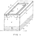
- Fig. 1 is a perspective view of a conventional MCT, which is disclosed in IEEE, 1991, pp. 138-141.
- impurities are diffused into the first major surface of an N ⁇ silicon semiconductor substrate 1 to form a P-type base region 2 and a P+-type emitter region 4, and an N-type emitter region 3 is formed in the P-type base region 2.
- semiconductor layers are grown in sequence on the second major surface, i.e., the undersurface of the semiconductor substrate 1 to form an N+-type layer 5 and a P+-type layer 6 serving as a buffer region and an undersurface P+-type emitter region, respectively.
- An anode electrode 10(A) is formed on the undersurface P+-type emitter region 6.
- a gate oxide film 7 is formed so as to overlap the N ⁇ -type semiconductor substrate 1, P-type base region 2, N-type emitter region 3, and P+-type emitter region 4.
- a polysilicon gate electrode 8(G) is formed on the gate oxide film 7. The gate oxide film 7 and gate electrode 8 are partially removed and opened to form a cathode electrode 9(K) in the opened area on the N-type emitter region 3 and P+-type emitter region 4.
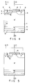
- a turn-off operation will be described with reference to Figs. 2 and 3.
- Fig. 2 when the anode A is positively biased and the cathode K is negatively biased, a positive voltage is applied to the gate G, an N-channel MOSFET constituted by the semiconductor substrate (N ⁇ -type base region) 1, P-type base region 2, and N-type emitter region 3 is operated to form an inversion layer 11 and inject electrons 12 from the N-type emitter region 3 into the N ⁇ -type base region 1.
- the electrons are injected into the N ⁇ -type base region 1, holes are injected from the undersurface P+-type emitter region 6 into the N ⁇ -type base region 1 to vary the conductivity.
- the MCT is thus turned on to cause the main current 16 to flow.
- the MCT is a self turn-off element capable of the turn-on and turn-off operations described above.
- the MCT has a drawback in which the turn-off operation is difficult to perform because the MCT tends to turn on in view of its operation characteristic.
- an improvement in turn-off characteristic is advanced.
- the concentrations of the P-type base region 2 and P+-type emitter region 4 have to increase.
- the discharge efficiency of the holes is influenced by the sheet resistances of the P-type base region 2 and P+-type emitter region 4.
- the concentrations of the P-type base region 2 and P+-type embitter region 4 have to increase, and the sheet resistances thereof have to decrease. If, however, the turn-off characteristic has priority over the turn-on characteristic and the P-type base region 2 is increased in concentration, the turn-on characteristic is deteriorated. More specifically, in the turn-on operation shown in Fig. 2, the N-channel MOSFET is operated to form the inversion layer 11, and the electrons are injected from the N-type emitter region 3 into the N ⁇ -type base region 1 to vary the conductivity and cause the main current to flow. If the concentration of the P-type base region is increased, the threshold voltage of the N-channel MOSFET is increased and the on-voltage is also increased, resulting in a great loss in the turn-on operation.
- the turn-on and turn-off characteristics of the MCT correlate with each other and, if one of the characteristics is improved, the other is deteriorated, which causes drawbacks wherein a trade-off is difficult between the turn-on and turn-off characteristics and the turn-off characteristic is difficult to improve.
- the conventional MCT is disclosed in Published Unexamined Japanese Patent Application No. 63-310171. According to this publication, a conventional five-layer structure is changed to a four-layer structure of pnpn to simplify a manufacturing process, and the short-circuit resistance of an emitter is lowered to perform a high-speed turn-off operation, but the drawback of difficulty in the trade-off between the turn-on and turn-off characteristics cannot be eliminated.
- An object of the present invention is to provide a semiconductor device which improves in trade-off between turn-on and turn-off characteristics and improves in the turn-off characteristic more than in a conventional device.
- a P ⁇ -type base region whose impurity concentration is lower than that of a P-type base region of a unit cell of an MCT is formed at an end portion of the P-type base region to form an initial operation region for a turn-on operation, and the efficiency of the turn-on operation is increased to improve a trade-off between the turn-on and turn-off characteristics.
- a semiconductor device comprises: a first semiconductor region of a first conductivity type exposed to a first major surface of a semiconductor substrate; a second semiconductor region of a second conductivity type formed in the first semiconductor region and exposed to the first major surface; a third semiconductor region of the first conductivity type formed in the second semiconductor region and exposed to the first major surface; a fourth semiconductor region of the second conductivity type formed in the first semiconductor region and exposed to the first major surface; a fifth semiconductor region of the second conductivity type formed in the first semiconductor region and exposed to a second major surface of the semiconductor substrate; a first electrode electrically connected to the third and fourth semiconductor regions; a gate electrode formed on the first major surface with a gate oxide film interposed therebetween and including a first region serving as an OFF gate region formed on a boundary between the first and second semiconductor regions, a boundary between the first and fourth semiconductor regions, and the first semiconductor region interposed between these boundaries, and a second region serving as an ON gate region formed on a boundary between the first and second semiconductor regions, a boundary between the second and
- a sixth semiconductor region is formed under the second region and its impurity concentration can be set lower than that of a portion of the second semiconductor region other than the sixth semiconductor region.
- the second semiconductor region covers an end of the third semiconductor region so as not to contact the third and sixth semiconductor regions each other in a region other than an ON-channel region.
- a contact portion of the third and sixth semiconductor regions can be set shorter than that of the second and third semiconductor regions on the first major surface of the semiconductor substrate.
- the semiconductor device comprises a seventh semiconductor region of the first conductivity type whose impurity concentration is higher than that of the first semiconductor region.
- the fifth semiconductor region exposed to the second major surface is formed directly under the second semiconductor region.
- a plurality of semiconductor devices each having the above structure are formed in a single semiconductor substrate, and the semiconductor substrate includes a first side on which an OFF-channel region is formed and a second side adjacent to the first side, on which an ON-channel region is formed.
- Fig. 6 is a schematic perspective view of a unit cell of a semiconductor device according to the first embodiment.
- N+- and P+-type epitaxial growing layers 5 and 6, which serve as an N+-type buffer region 5 and an undersurface P+-type emitter region 6, are formed on the undersurface, i.e., the second major surface of an N ⁇ -type silicon semiconductor substrate 1, and an anode electrode 19(A) is formed on the undersurface P+-type emitter region 6.
- the structure on the second major surface of the semiconductor substrate is the same as that in the conventional MCT describe above (Fig. 1).
- a P-type base region 2 is formed in the semiconductor substrate 1, an N-type emitter region 3 is formed in the base region 2, and a P-type emitter region 4 is formed in an N ⁇ -type base region 1 of the semiconductor substrate.
- the N-type emitter region 3, P-type base region 2, N ⁇ -type base region 1, and P-type emitter region 4 serve as third, second, first and fourth semiconductor regions, respectively, and exposed to the first major surface.
- the second semiconductor region (P-type base region 2) includes a low-concentration region 17, and is interposed between the first semiconductor region (N ⁇ -type base region 1) and the third semiconductor region (N-type emitter region 3) near its exposed portion.
- An electrode 8(G) is formed on the first major surface with a cathode electrode 9(K) and a gate oxide film 7 interposed therebetween.
- the gate electrode 8(G) includes first and second regions.
- the first region Goff (OFF gate region) is formed on the N ⁇ -type base region 1 interposed between a boundary between the N ⁇ -type base region 1 and P-type base region 2 and a boundary between the N ⁇ -type base region 1 and P-type emitter region 4.
- the second region Gon (ON gate region), which is spaced away from the first region Goff, is formed on the P ⁇ -type base region 17 interposed between a boundary between the N ⁇ -type base region 1 and P ⁇ -type base region 17 and a boundary between the P ⁇ -type base region 17 and N-type emitter region 3.
- the N+- and P+-type layers are grown on the second major surface of the N ⁇ -type silicon semiconductor substrate 1 to form the N+-type buffer region 5 and undersurface P+-type emitter region 6.
- the semiconductor substrate serves as an N ⁇ -type base region 1, a silicon oxide film and a polysilicon film are formed on the first major surface of the substrate using a well-known technique, and these films are selectively etched to form the gate oxide film 7 and gate electrode 8(G). Impurities are then diffused from the first major surface into a part of the N ⁇ -type base region 1 to form the P ⁇ -type base region 17.
- Impurities are diffused into another part of the base region 1 and the base region 17 to form the P-type emitter region 4 on the N ⁇ -type base region 1 and the P-type base region 2 on the P - -type base region 17.
- the N-type emitter region 3 is formed in the P-type base region 2. These diffusion regions are formed by ion-implantation, and the gate electrode is then used as a mask. Since the N-type emitter region 3 is formed so as to somewhat intrude to the inner side of the first region Goff (OFF gate region) of the gate electrode 8, the first region Goff is formed to overlap the N-type emitter region 3, P-type base region 2, N ⁇ base region 1, and P-type emitter region 4.
- the gate electrode does not have to overlap the N-type emitter region 3 since only a channel formed between the P-type base and emitter regions 2 and 4 is necessary.
- the first region Goff has only to cover the P-type base region 2, N ⁇ -type base region 1, and P-type emitter region 4.
- the silicon oxide film is partially opened to form the cathode electrode 9(K) on the N- and P-type emitter regions 3 and 4 and to form the anode electrode 10(A) on the undersurface of the semiconductor substrate.
- the N+-type buffer region 5 and undersurface P+-type emitter region 6 can be formed by diffusing impurities into the semiconductor substrate.
- the feature of the semiconductor device according to the first embodiment lies in that the P ⁇ -type base region 17 of low concentration is formed at one end of the P-type base region 2 in the longitudinal direction of the cell of the semiconductor device.
- the N ⁇ -type silicon substrate is used in the first embodiment, a P+-type silicon substrate can be substituted therefor. More specifically, the N+-type buffer region 5 and the N ⁇ -type base region 1 are grown in sequence on the P+-type silicon semiconductor substrate serving as the P+-type emitter region 6. Then, the P-type base region 2 and P-type emitter region 4 are formed by diffusion on the surface of the N ⁇ -type base region 1, and the N-type emitter region 3 is formed by diffusion in the P-type base region 2.
- the method of forming the other regions is the same as that in the first embodiment. This method is well-known and can be applied to the following embodiments.
- the P ⁇ -type base region 17 is formed at the end of the P-type base region 2, even when the impurity concentration of the P-type base region 2 is increased to improve the turn-off characteristic, an N-channel MOSFET serving as a switch for a turn-on operation is always formed in the P ⁇ -type base region 17, and thus its threshold voltage is not increased.
- the turn-on operation is performed in the N-type emitter region 3 serving as an initial operating region, near the P ⁇ -type base region, and extends to the central part of the N-type emitter region 1.
- the N-channel MOSFET always operates at a constant threshold voltage
- the turn-on operation is performed in a region of low on-voltage serving as an initial operating region, and a region for the turn-on operation extends, thereby controlling the on-voltage. It is thus possible to improve the trade-off between the turn-on and turn-off operations of the MCT of the present invention.
- the length of the cell is adjusted to determine the ratio of the length to the width of the cell and the concentration of the base region; therefore, the trade-off between them is improved, and the turn-off characteristic can be improved.
- Figs. 7 to 9 show the turn-off operation of the cell, in which Fig. 7 is a perspective view of the cell, and Figs. 8 and 9 are cross-sectional views taken along line Y - Y' in Fig. 7.
- a positive bias is applied to the anode A and a negative bias is applied to the cathode K to positively bias the gate.
- An inversion layer 18 is thus formed in the P ⁇ -type base region 17.
- the N-channel MOSFET is operated in this base region 17, and electrons are injected from the N-type emitter region 3 to the N ⁇ -type base region 1.
- Holes 13 are thus injected from the P+-type undersurface emitter region 6 to vary the conductivity.
- Fig. 10 is a perspective view of the cell of the semiconductor device for explaining the turn-off operation.
- a positive bias is applied to the anode A and a negative bias is applied to the cathode K, and the gate G is negatively biased while the main current is flowing.
- the P-channel MOSFET is operated to form an inversion layer 20, the P-type base and emitter regions 2 and 4, and the cathode electrode 9 are short-circuited, and holes 16 of the main current are discharged from the cathode electrode 9. Therefore, electrons are prevented from being injected from the N-type emitter region 3, and the main current 14(I) does not flow, resulting in completion of the turn-off operation.
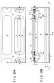
- Figs. 11 and 13 are schematic plan views which respectively show initial operation regions of the semiconductor substrate for the turn-on and turn-off operations.
- the initial operation regions 21 for the turn-on operation are formed at both ends of the N-type emitter region 3 in the vicinity of the P ⁇ -type base region 17, and the initial operation region 22 for the turn-off operation is formed along a connecting portion of the N-type emitter region 3 and the P-type base region 2. Since the turn-on operation starts from both the ends of the N-type emitter region 3 and extends to the center thereof, the present invention differs from the conventional MCT (Fig. 1) whose turn-on and turn-off operations both start from the N-type emitter region 3 contacting the P-type base region 2.
- the boundary between the N-type emitter region 3 and P-type base region 2, and the P ⁇ -type base region 17, will be described.
- the P-type base region 2 and the N-type emitter region 3 formed therein are lengthened in the same direction.
- the initial operation region 21 for the turn-on operation can be shortened as much as possible.
- the longer the initial operation region 22 for the turn-off operation the better the turn-off characteristic.
- h is about 5 ⁇ m, however, it can be set to 1 to 10 ⁇ m.
- the ratio of h to H is about 1 to 5 in this embodiment, however, it can be about 1 to 10 to improve the turn-off characteristic and can be about 1 to 3 to maintain the turn-on characteristic, at a little sacrifice of the turn-off characteristic.
- the P ⁇ -type base regions 17 are formed so as to cover both the ends of the P-type base region 2, that is, to cover the short sides of the N-type emitter region 3, and the P-type base region is formed so as to surround both the ends of the N-type emitter region 3, thereby preventing the N-type emitter region 3 and P ⁇ -type base region 17 from contacting each other. If these regions 3 and 17 are formed to contact each other, the P ⁇ -type base region 17 affects the turn-off operation, and a conductive region in which holes are difficult to move when discharged in the turn-off operation, is easy to remain, thereby degrading the turn-off characteristic.
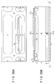
- Fig. 12 is a cross-sectional view showing the side of the MCT in Fig.
- Fig. 14 is also a cross-sectional view showing the side of the MCT in which an OFF gate region is formed.
- the gate electrode 8 and the cathode electrode 9 are insulated from each other by an interlayer insulation film.
- Fig. 21 is a characteristic diagram in which an abscissa indicates on-voltage (V) and an ordinate indicates on-current (A/cm2).
- Curves A, B, C and D show the current-voltage characteristics which are obtained when the impurity concentration of the N-type emitter region 3 is 2 x 10²⁰/cm2, and that of the P-type base region 2 is 1.0 x 10¹⁷/cm2, 2.0 x 10¹⁸/cm2, 4.0 x 10¹⁸/cm2, and 5.0 x 10¹⁸/cm2, respectively. If the impurity concentration of the P ⁇ -type base region 17 is lower, the current-voltage characteristic is improved. More specifically, if the impurity concentration of the region 17 is lower, a large amount of current can be caused to flow at a low voltage. Therefore, the turn-on characteristic is improved by forming the ON gate region of the P-type base region 2.
- Fig. 22 is a perspective view of an MCT chip of the semiconductor device according to the present invention, which is formed from the semiconductor substrate having a plurality of cells.
- a plurality of pairs of P-type emitter regions 4 and P-type base regions including the P ⁇ -type base regions 17 are formed in matrix on the first major surface of the semiconductor substrate, and the electrodes of the cells are connected to one another to form the gate G and cathode K of the MCT chip on the surface of the semiconductor substrate.
- the electrodes of the cells are connected to one another to form the gate G and cathode K of the MCT chip on the surface of the semiconductor substrate.
- an off-channel is formed in the N ⁇ -type base region 1 between the P-type base and emitter regions 2 and 4 under the Off gate region of the gate electrode, and an on-channel region is formed in the P ⁇ -type base region 17 between the N ⁇ -type base region 1 and N-type emitter region 3 under the ON gate region of the gate electrode.
- the size of the chip is about 2 to 4 mm.
- Fig. 15 is a schematic perspective view of an MCT according to the second embodiment of the present invention
- Figs. 16 and 17 are perspective views of the MCT to explain the turn-on and turn-off operation of the MCT.
- a P ⁇ -type silicon semiconductor substrate is substituted for the N ⁇ -type silicon semiconductor substrate of the MCT of the first embodiment.
- a P+-type buffer region 28 and an undersurface N+-type emitter region 29 are formed on the second major surface of a P ⁇ -type silicon semiconductor substrate 23.
- a gate oxide film 30 and a polysilicon gate electrode 31 are formed on the second major surface of the semiconductor substrate, and then impurities are diffused to form an N ⁇ -type base region 24, an N-type base region 25, a P-type emitter region 26, and an N-type emitter region 27.
- the gate oxide film 30 is partially opened to form an anode electrode 32, and a cathode electrode 33 is formed on the second major surface of the semiconductor substrate.
- a turn-on operation and a turn-off operation of the MCT according to the second embodiment will be described.
- a positive bias is applied to the anode A
- a negative bias is applied to the cathode K
- a negative bias is applied to the gate G
- a P-channel MOSFET is operated to form an inversion layer 36.
- holes 34 are injected into the P ⁇ -type base region 23 and electrons 35 are injected from the undersurface N+-type emitter region 29. Therefore, the conductivity of the MCT varies in the P ⁇ -type base region 1, and the MCT turns on to cause the main current to flow.
- a positive bias is applied to the anode A
- a negative bias is applied to the cathode K
- a positive bias is applied to the gate while the main current 37 is flowing.
- the N-channel MOSFET is thus operated to form an inversion layer 39.
- the N-type base and emitter regions 25 and 27, and the anode electrode 32 are short-circuited to discharge electrons 38 from the main current and prevent the holes from being injected from the P-type emitter region 26.
- the main current is thus stopped. Only the relationship between injection and discharge of carriers in the second embodiment is opposite to that in the first embodiment, and the turn-on and turn-off characteristics of the second embodiment is the same as those of the first embodiment.
- FIG. 18 is a schematic perspective view of an MCT according to the third embodiment
- Figs. 19 and 20 are also schematic perspective views of the MCT to explain its turn-on and turn-off operations.
- the structure of this MCT is called an anode short structure in which an undersurface P+-type emitter region and an undersurface N+-type buffer region are short-circuited each other.
- An undersurface P+-type emitter region 40 and an N+-type buffer region 41 are formed on the second major surface of the N ⁇ -type silicon semiconductor substrate 1, and the gate oxide film 7 and polysilicon gate electrode 8 are formed on the first major surface of the substrate 1.
- Impurities are diffused from the first major surface to the semiconductor substrate 1 to form the P ⁇ -type base region 17, P-type base region 2, and N-type emitter region 3.
- the gate oxide film is partially opened to form the cathode electrode 9, and the anode electrode 10 is formed on the undersurface of the substrate.
- the turn-on and turn-off operations of the MCT according to the third embodiment are the same as those of the MCT according to the first embodiment. Since, however, the MCT of the third embodiment has the anode short structure, holes are injected from the undersurface P+-type emitter region 40 formed directly under the P ⁇ -type base region 17, and the turn-on operation is performed.
- Fig. 23 is a schematic perspective view of an MCT according to the fourth embodiment of the present invention.
- the structure of the MCT of the fourth embodiment is the same as that of the MCT of the first embodiment, except for the first region Goff (OFF gate region) of the gate electrode 8.
- the first region Goff is formed on the N-type emitter region 3. Since the gate is used as a mask when the region 3 is formed by diffusion of impurities, it is unavoidable that the region 3 slightly goes under the gate. Actually, the gate above the region 3 is unnecessary since this portion is used only to turn off the gate (only the off-channel formed in the N ⁇ -type base region 1 is necessary).
- the gate above the N-type emitter region 3 is removed, and the gate oxide film 7 is exposed.
- the present invention can be applied to a double gate structure.
- silicon is used as a semiconductor.
- the silicon can be replaced with well-known materials such as Ge and GaAs.
- the impurity concentration of the P-type base region can be varied from place to place, the trade-off between the turn-on and turn-off characteristics can be performed satisfactorily, and the turn-off efficiency can be enhanced.
- Fig. 24 is a schematic perspective view of an MCT according to a fifth embodiment of the present invention
- Figs. 25 and 26 are views for explaining turn-on and turn-off operations of the MCT shown in Fig. 24.
- An N+-type buffer layer 6 is formed on an N ⁇ -type semiconductor substrate 1, an undersurface P+-type emitter layer 7 is formed on the layer 6, and P-type base and drain regions 2 and 4 are formed in the substrate 1 by diffusion of impurities.
- P-type deposition layers are formed on the surfaces of the regions 2 and 4.
- An N ⁇ -type epitaxial layer of about 1 ⁇ m is grown on the surface portion of the substrate 1, a gate oxide film 8 and a polysilicon gate electrode 9 are formed on the surface of the N ⁇ -type epitaxial layer, and a P ⁇ -type base region 3 and an N-type emitter region 5 are formed in the N ⁇ -type epitaxial layer by diffusion of impurities.
- the P ⁇ -type base region 3 which was conventionally formed to the same depth as that of the P-type base region, can be formed in only the surface portion of an end portion of the P-type base region.
- the MCT can be manufactured by a burying diffusion method or a method using a bonded wafer as well as the above method using the epitaxial layer.
- an N-channel inversion layer 12 is formed on the surface of the P ⁇ -type base region 3, and electrons are injected from the N-type emitter region 5 into the N ⁇ -type base region 1. Holes 14 are then injected into the N ⁇ -type base region 1 from the undersurface P+-type emitter layer 7. Therefore, the conductivity of the N ⁇ -type base region 1 varies, and the electrons are directly injected from the N-type emitter region 5 into the N ⁇ -type base region 1 through the P-type base region 2.
- the turn-on operation starts from an N-type emitter region 15 near the P ⁇ -type base region 3 and extends to the central part of the N-type emitter region 5, thereby turning on the MCT.
- the anode electrode When the anode electrode is positively biased, the cathode electrode is negatively biased, and the gate electrode is negatively biased while a main current 17 is flowing, the N-channel inversion layer 12 formed in the turn-on operation is vanished, and a P-channel inversion layer 16 is formed on the N ⁇ -type base region 1 between the P-type base and drain regions.
- the P-type base and drain regions and the cathode electrode are short-circuited, and holes 16 of the main current 17 are discharged from the cathode electrode.
- electrons are stopped from being injected from the N-type emitter region 5, and the main current is prevented from flowing.
- the turn-off operation starts from a region 19 facing the P-type drain region 4 and the N-type emitter region 5, and finally extends to the entire N-type emitter region 5, thereby turning off the MCT.
- the MCT according to the fifth embodiment can be applied to a double gate structure and a structure in which the N ⁇ -type substrate is changed to a P ⁇ -type substrate, and on- and off-channel regions serve as P- and N-channel MOSFETs, respectively.
- an MCT having ON and OFF gate regions which are formed separately from each other, can be applied to the present invention.
- the advantage of the MCT according to the fifth embodiment of the present invention is to improve the turn-off characteristic.
- the turn-off characteristic is improved, using a method of efficiently discharging holes by increasing the concentrations of the P-type base and drain regions 2 and 4 and decreasing the resistances of current paths of the P-type base region, P-channel inversion layer, P-type drain region, and cathode electrode, through which the holes are discharged.
- the P ⁇ -type base region is formed in only the surface portion of an end portion of the P-type base region. If the P ⁇ -type base region is formed in only the surface portion of an end portion of the P-type base region in which the N-channel inversion layer is to be formed in the turn-on operation, the resistance of the path through which the hole current flows in the turn-off operation, is decreased, and the current easily flow.
- the P ⁇ -type base region 3 is formed in the surface portion of the P-type base region 2 so as to extend from a junction between the P-type base region 2 and the N-type emitter region 5 to a junction between the P-type base region 2 and the N-type base region 1.
- the P ⁇ -type base region 3 is thus formed in the portion where the N-channel inversion layer 12 is formed in the turn-on operation.
- the anode electrode is positively biased, the cathode electrode is negatively biased, and the gate is negatively biased while the main current is flowing.
- the P-channel inversion layer 16 is formed on the surface of the N ⁇ -type base region between the P-type base and drain regions, the P-type base and drain regions and the cathode electrode are short-circuited, and the holes 16 of the main current are discharged from the cathode electrode.
- the electrons are stopped from being injected from the N-type emitter region 5. Since, in this time, the P ⁇ -type base region 3 is surrounded with the P-type base region 2 at a junction between the end portion of the P-type base region 2 and the N-type emitter region 5, the N-channel inversion layer 12 formed in the turn-on operation is vanished, and the electrons are easy to stop, thereby improving the turn-off characteristic of the MCT.
- the P ⁇ -type base region is formed in the entire end portion of the P-type base region which contacts the N-type emitter region.
- the P ⁇ -type base region 3 is formed in only the surface portion of the end portion of the P-type base region 2, so that the injection of electrons is controlled, and the turn-off characteristic is improved.
- the characteristic of the N-channel MOSFET is the same as that in the conventional MCT, and the electrons are sufficiently injected from the N-channel inversion layer into the N ⁇ -type base region 1. Therefore, the same turn-on operation as that of the conventional MCT is performed, and the turn-on characteristic is the same as that in the conventional MCT.
- the turn-off characteristic can be improved, without degrading the turn-on characteristic.
- the tradeoff between the turn-on and turn-off characteristics in a device design is improved.
Abstract
Description
- The present invention relates to a structure of a MOS gate controlled thyristor (hereinafter referred to as MCT) capable of turning on/off a MOS gate by changing a polarity of voltage applied thereto.
- The MCT is a thyristor whose emitter and base have the same conductivity type and are short-circuited by a MOS gate type transistor when a voltage is applied to a gate electrode of the transistor. This turn-off operation requires a small amount of gate power only because the thyristor controls power consumption, and no self-turn-off operation can be performed in this thyristor. Therefore, a MOS type thyristor is known in which a control electrode is provided at a base whose conductivity type is opposite to that of the above base, and a negative bias is applied to the control electrode to discharge part of anode current as base current, thereby performing a self-turn-off operation.
- Fig. 1 is a perspective view of a conventional MCT, which is disclosed in IEEE, 1991, pp. 138-141. As shown in Fig. 1, impurities are diffused into the first major surface of an N⁻
silicon semiconductor substrate 1 to form a P-type base region 2 and a P⁺-type emitter region 4, and an N-type emitter region 3 is formed in the P-type base region 2. Further, semiconductor layers are grown in sequence on the second major surface, i.e., the undersurface of thesemiconductor substrate 1 to form an N⁺-type layer 5 and a P⁺-type layer 6 serving as a buffer region and an undersurface P⁺-type emitter region, respectively. An anode electrode 10(A) is formed on the undersurface P⁺-type emitter region 6. On the first major surface, agate oxide film 7 is formed so as to overlap the N⁻-type semiconductor substrate 1, P-type base region 2, N-type emitter region 3, and P⁺-type emitter region 4. A polysilicon gate electrode 8(G) is formed on thegate oxide film 7. Thegate oxide film 7 andgate electrode 8 are partially removed and opened to form a cathode electrode 9(K) in the opened area on the N-type emitter region 3 and P⁺-type emitter region 4. - An operation (turn-on and turn-off) of the above conventional MCT will now be described.
- First a turn-off operation will be described with reference to Figs. 2 and 3. As shown in Fig. 2, when the anode A is positively biased and the cathode K is negatively biased, a positive voltage is applied to the gate G, an N-channel MOSFET constituted by the semiconductor substrate (N⁻-type base region) 1, P-
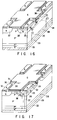
type base region 2, and N-type emitter region 3 is operated to form aninversion layer 11 and injectelectrons 12 from the N-type emitter region 3 into the N⁻-type base region 1. As shown in Fig. 3, since the electrons are injected into the N⁻-type base region 1, holes are injected from the undersurface P⁺-type emitter region 6 into the N⁻-type base region 1 to vary the conductivity. The MCT is thus turned on to cause themain current 16 to flow. - Next a turn-off operation will be described with reference to Figs. 4 and 5. When the anode A is positively biased, the cathode K is negatively biased, and the main current 14 flows, a negative bias is applied to the gate G, and a P-channel MOSFET constituted by the N⁻-
type base region 1, P-type base region 2, and P⁺-type emitter region 4 is operated to form aninversion layer 15. Therefore, the P-type base region 2 andcathode electrode 9 are short-circuited, and the P⁺-type emitter region 4 andcathode electrode 9 are short-circuited, andholes 16 in the main current are discharged from these paths connecting theregions cathode electrode 9. When theholes 16 are discharged, the electrons are prevented from flowing from the N-type emitter region 3, and the main current is stopped. The turn-off operation is thus completed. The MCT is a self turn-off element capable of the turn-on and turn-off operations described above. - However, the MCT has a drawback in which the turn-off operation is difficult to perform because the MCT tends to turn on in view of its operation characteristic. At present, an improvement in turn-off characteristic is advanced. To improve the turn-off characteristic of the MCT, the concentrations of the P-
type base region 2 and P⁺-type emitter region 4 have to increase. In the turn-off operation shown in Figs. 3 and 4, when the holes are discharged from the main current to thecathode electrode 9 by virtue of theinversion layer 15 formed by the operation of the P-channel MOSFET, the discharge efficiency of the holes is influenced by the sheet resistances of the P-type base region 2 and P⁺-type emitter region 4. To improve the discharge efficiency, the concentrations of the P-type base region 2 and P⁺-type embitter region 4 have to increase, and the sheet resistances thereof have to decrease. If, however, the turn-off characteristic has priority over the turn-on characteristic and the P-type base region 2 is increased in concentration, the turn-on characteristic is deteriorated. More specifically, in the turn-on operation shown in Fig. 2, the N-channel MOSFET is operated to form theinversion layer 11, and the electrons are injected from the N-type emitter region 3 into the N⁻-type base region 1 to vary the conductivity and cause the main current to flow. If the concentration of the P-type base region is increased, the threshold voltage of the N-channel MOSFET is increased and the on-voltage is also increased, resulting in a great loss in the turn-on operation. - As described above, the turn-on and turn-off characteristics of the MCT correlate with each other and, if one of the characteristics is improved, the other is deteriorated, which causes drawbacks wherein a trade-off is difficult between the turn-on and turn-off characteristics and the turn-off characteristic is difficult to improve. The conventional MCT is disclosed in Published Unexamined Japanese Patent Application No. 63-310171. According to this publication, a conventional five-layer structure is changed to a four-layer structure of pnpn to simplify a manufacturing process, and the short-circuit resistance of an emitter is lowered to perform a high-speed turn-off operation, but the drawback of difficulty in the trade-off between the turn-on and turn-off characteristics cannot be eliminated.
- An object of the present invention is to provide a semiconductor device which improves in trade-off between turn-on and turn-off characteristics and improves in the turn-off characteristic more than in a conventional device.
- According to the present invention, a P⁻-type base region whose impurity concentration is lower than that of a P-type base region of a unit cell of an MCT, is formed at an end portion of the P-type base region to form an initial operation region for a turn-on operation, and the efficiency of the turn-on operation is increased to improve a trade-off between the turn-on and turn-off characteristics.
- A semiconductor device according to the present invention comprises:
a first semiconductor region of a first conductivity type exposed to a first major surface of a semiconductor substrate;
a second semiconductor region of a second conductivity type formed in the first semiconductor region and exposed to the first major surface;
a third semiconductor region of the first conductivity type formed in the second semiconductor region and exposed to the first major surface;
a fourth semiconductor region of the second conductivity type formed in the first semiconductor region and exposed to the first major surface;
a fifth semiconductor region of the second conductivity type formed in the first semiconductor region and exposed to a second major surface of the semiconductor substrate;
a first electrode electrically connected to the third and fourth semiconductor regions;
a gate electrode formed on the first major surface with a gate oxide film interposed therebetween and including a first region serving as an OFF gate region formed on a boundary between the first and second semiconductor regions, a boundary between the first and fourth semiconductor regions, and the first semiconductor region interposed between these boundaries, and a second region serving as an ON gate region formed on a boundary between the first and second semiconductor regions, a boundary between the second and third semiconductor regions, and the second semiconductor region interposed between these boundaries; and
a second electrode formed on the fifth semiconductor region. - A sixth semiconductor region is formed under the second region and its impurity concentration can be set lower than that of a portion of the second semiconductor region other than the sixth semiconductor region. The second semiconductor region covers an end of the third semiconductor region so as not to contact the third and sixth semiconductor regions each other in a region other than an ON-channel region. A contact portion of the third and sixth semiconductor regions can be set shorter than that of the second and third semiconductor regions on the first major surface of the semiconductor substrate. Further, the semiconductor device comprises a seventh semiconductor region of the first conductivity type whose impurity concentration is higher than that of the first semiconductor region. The fifth semiconductor region exposed to the second major surface is formed directly under the second semiconductor region.
- A plurality of semiconductor devices each having the above structure, are formed in a single semiconductor substrate, and the semiconductor substrate includes a first side on which an OFF-channel region is formed and a second side adjacent to the first side, on which an ON-channel region is formed.
- Since an initial turn-on region for the turn-on operation is formed away from that for the turn-off operation, the impurity concentration of the P-type base region is partially changed to improve the turn-on characteristic.
- This invention can be more fully understood from the following detailed description when taken in conjunction with the accompanying drawings, in which:
- Fig. 1 is a schematic perspective view of a conventional MCT;
- Figs. 2 and 3 are cross-sectional views taken along line X - X' of Fig. 1 to explain a turn-on operation of the conventional MCT;
- Figs. 4 and 5 are cross-sectional views taken along line X - X' of Fig. 1 to explain a turn-off operation of the conventional MCT;
- Fig. 6 is a perspective view of an MCT according to a first embodiment of the present invention;
- Fig. 7 is a schematic perspective view for explaining a turn-on operation of the MCT shown in Fig. 6;
- Figs. 8 and 9 are cross-sectional views taken along line Y - Y' of Fig. 7 to explain the turn-on operation of the MCT;
- Fig. 10 is a perspective view for explaining a turn-off operation of the MCT shown in Fig. 6;
- Fig. 11 is a plan view of a semiconductor device for explaining the turn-on operation of the MCT shown in Fig. 6;
- Fig. 12 is a cross-sectional view of the semiconductor device shown in Fig. 11;
- Fig. 13 is a plan view of a semiconductor device for explaining the turn-off operation of the MCT shown in Fig. 6;
- Fig. 14 is a cross-sectional view of the semiconductor device shown in Fig. 13;
- Fig. 15 is a perspective view of an MCT according to a second embodiment of the present invention;
- Fig. 16 is a perspective view for explaining a turn-on operation of the MCT shown in Fig. 15;
- Fig. 17 is a perspective view for explaining a turn-off operation of the MCT shown in Fig. 15;
- Fig. 18 is a perspective view of an MCT according to a third embodiment of the present invention;
- Fig. 19 is a perspective view for explaining a turn-on operation of the MCT shown in Fig. 18;
- Fig. 20 is a perspective view for explaining a turn-off operation of the MCT shown in Fig. 18;
- Fig. 21 is a graph showing impurity concentration dependence of the turn-on operation of the MCT of the present invention;
- Fig. 22 is a perspective view of the MCT having a plurality of cells according to the present invention;
- Fig. 23 is a perspective view of an MCT according to a fourth embodiment of the present invention; and
- Fig. 24 is a schematic perspective view of an MCT according to a fifth embodiment of the present invention;
- Figs. 25A, 25B and 25C and 26A, 26B and 26C are views for explaining turn-on and turn-off operations of the MCT shown in Fig. 24; and
- Fig. 27 is a schematic perspective view of an MCT according to a sixth embodiment of the present invention.
- Embodiments of the present invention will now be described, with reference to the accompanying drawings. A first embodiment of the present invention will be described with reference to Figs. 6 to 14. Fig. 6 is a schematic perspective view of a unit cell of a semiconductor device according to the first embodiment. As shown in Fig. 6, N⁺- and P⁺-type
epitaxial growing layers type buffer region 5 and an undersurface P⁺-type emitter region 6, are formed on the undersurface, i.e., the second major surface of an N⁻-typesilicon semiconductor substrate 1, and an anode electrode 19(A) is formed on the undersurface P⁺-type emitter region 6. The structure on the second major surface of the semiconductor substrate is the same as that in the conventional MCT describe above (Fig. 1). On the first major surface side, a P-type base region 2 is formed in thesemiconductor substrate 1, an N-type emitter region 3 is formed in thebase region 2, and a P-type emitter region 4 is formed in an N⁻-type base region 1 of the semiconductor substrate. The N-type emitter region 3, P-type base region 2, N⁻-type base region 1, and P-type emitter region 4 serve as third, second, first and fourth semiconductor regions, respectively, and exposed to the first major surface. The second semiconductor region (P-type base region 2) includes a low-concentration region 17, and is interposed between the first semiconductor region (N⁻-type base region 1) and the third semiconductor region (N-type emitter region 3) near its exposed portion. An electrode 8(G) is formed on the first major surface with a cathode electrode 9(K) and agate oxide film 7 interposed therebetween. The gate electrode 8(G) includes first and second regions. The first region Goff (OFF gate region) is formed on the N⁻-type base region 1 interposed between a boundary between the N⁻-type base region 1 and P-type base region 2 and a boundary between the N⁻-type base region 1 and P-type emitter region 4. The second region Gon (ON gate region), which is spaced away from the first region Goff, is formed on the P⁻-type base region 17 interposed between a boundary between the N⁻-type base region 1 and P⁻-type base region 17 and a boundary between the P⁻-type base region 17 and N-type emitter region 3. - A process of manufacturing the semiconductor device will be described. The N⁺- and P⁺-type layers are grown on the second major surface of the N⁻-type
silicon semiconductor substrate 1 to form the N⁺-type buffer region 5 and undersurface P⁺-type emitter region 6. The semiconductor substrate serves as an N⁻-type base region 1, a silicon oxide film and a polysilicon film are formed on the first major surface of the substrate using a well-known technique, and these films are selectively etched to form thegate oxide film 7 and gate electrode 8(G). Impurities are then diffused from the first major surface into a part of the N⁻-type base region 1 to form the P⁻-type base region 17. Impurities are diffused into another part of thebase region 1 and thebase region 17 to form the P-type emitter region 4 on the N⁻-type base region 1 and the P-type base region 2 on the P - -type base region 17. The N-type emitter region 3 is formed in the P-type base region 2. These diffusion regions are formed by ion-implantation, and the gate electrode is then used as a mask. Since the N-type emitter region 3 is formed so as to somewhat intrude to the inner side of the first region Goff (OFF gate region) of thegate electrode 8, the first region Goff is formed to overlap the N-type emitter region 3, P-type base region 2, N⁻base region 1, and P-type emitter region 4. However, the gate electrode does not have to overlap the N-type emitter region 3 since only a channel formed between the P-type base andemitter regions type base region 2, N⁻-type base region 1, and P-type emitter region 4. The silicon oxide film is partially opened to form the cathode electrode 9(K) on the N- and P-type emitter regions type buffer region 5 and undersurface P⁺-type emitter region 6 can be formed by diffusing impurities into the semiconductor substrate. The feature of the semiconductor device according to the first embodiment lies in that the P⁻-type base region 17 of low concentration is formed at one end of the P-type base region 2 in the longitudinal direction of the cell of the semiconductor device. - Though the N⁻-type silicon substrate is used in the first embodiment, a P⁺-type silicon substrate can be substituted therefor. More specifically, the N⁺-
type buffer region 5 and the N⁻-type base region 1 are grown in sequence on the P⁺-type silicon semiconductor substrate serving as the P⁺-type emitter region 6. Then, the P-type base region 2 and P-type emitter region 4 are formed by diffusion on the surface of the N⁻-type base region 1, and the N-type emitter region 3 is formed by diffusion in the P-type base region 2. The method of forming the other regions is the same as that in the first embodiment. This method is well-known and can be applied to the following embodiments. - Since the P⁻-
type base region 17 is formed at the end of the P-type base region 2, even when the impurity concentration of the P-type base region 2 is increased to improve the turn-off characteristic, an N-channel MOSFET serving as a switch for a turn-on operation is always formed in the P⁻-type base region 17, and thus its threshold voltage is not increased. The turn-on operation is performed in the N-type emitter region 3 serving as an initial operating region, near the P⁻-type base region, and extends to the central part of the N-type emitter region 1. More specifically, even though the impurity concentration of the P-type base region varies, the N-channel MOSFET always operates at a constant threshold voltage, the turn-on operation is performed in a region of low on-voltage serving as an initial operating region, and a region for the turn-on operation extends, thereby controlling the on-voltage. It is thus possible to improve the trade-off between the turn-on and turn-off operations of the MCT of the present invention. Furthermore, the length of the cell is adjusted to determine the ratio of the length to the width of the cell and the concentration of the base region; therefore, the trade-off between them is improved, and the turn-off characteristic can be improved. - An operation of the cell of the semiconductor device according to the first embodiment will be described in detail, with reference to Figs. 7 to 14. Figs. 7 to 9 show the turn-off operation of the cell, in which Fig. 7 is a perspective view of the cell, and Figs. 8 and 9 are cross-sectional views taken along line Y - Y' in Fig. 7. A positive bias is applied to the anode A and a negative bias is applied to the cathode K to positively bias the gate. An
inversion layer 18 is thus formed in the P⁻-type base region 17. The N-channel MOSFET is operated in thisbase region 17, and electrons are injected from the N-type emitter region 3 to the N⁻-type base region 1.Holes 13 are thus injected from the P⁺-typeundersurface emitter region 6 to vary the conductivity. First the P⁻-type base region 17 is turned on and changed to an initial turn-onregion 19, and then a region for the turn-operation extends to the central part of the cell, thereby completely turning on the cell. - Fig. 10 is a perspective view of the cell of the semiconductor device for explaining the turn-off operation. A positive bias is applied to the anode A and a negative bias is applied to the cathode K, and the gate G is negatively biased while the main current is flowing. The P-channel MOSFET is operated to form an
inversion layer 20, the P-type base andemitter regions cathode electrode 9 are short-circuited, and holes 16 of the main current are discharged from thecathode electrode 9. Therefore, electrons are prevented from being injected from the N-type emitter region 3, and the main current 14(I) does not flow, resulting in completion of the turn-off operation. - Figs. 11 and 13 are schematic plan views which respectively show initial operation regions of the semiconductor substrate for the turn-on and turn-off operations. The
initial operation regions 21 for the turn-on operation are formed at both ends of the N-type emitter region 3 in the vicinity of the P⁻-type base region 17, and theinitial operation region 22 for the turn-off operation is formed along a connecting portion of the N-type emitter region 3 and the P-type base region 2. Since the turn-on operation starts from both the ends of the N-type emitter region 3 and extends to the center thereof, the present invention differs from the conventional MCT (Fig. 1) whose turn-on and turn-off operations both start from the N-type emitter region 3 contacting the P-type base region 2. - Referring to Figs. 11 to 14, the boundary between the N-
type emitter region 3 and P-type base region 2, and the P⁻-type base region 17, will be described. As shown in Figs. 11 and 12, the P-type base region 2 and the N-type emitter region 3 formed therein, are lengthened in the same direction. Theinitial operation region 21 for the turn-on operation can be shortened as much as possible. The longer theinitial operation region 22 for the turn-off operation, the better the turn-off characteristic. If, therefore, the ratio of theseregions type base regions 17 are formed so as to cover both the ends of the P-type base region 2, that is, to cover the short sides of the N-type emitter region 3, and the P-type base region is formed so as to surround both the ends of the N-type emitter region 3, thereby preventing the N-type emitter region 3 and P⁻-type base region 17 from contacting each other. If theseregions type base region 17 affects the turn-off operation, and a conductive region in which holes are difficult to move when discharged in the turn-off operation, is easy to remain, thereby degrading the turn-off characteristic. Fig. 12 is a cross-sectional view showing the side of the MCT in Fig. 11 in which an ON gate region of thegate electrode 8 is formed, and Fig. 14 is also a cross-sectional view showing the side of the MCT in which an OFF gate region is formed. Thegate electrode 8 and thecathode electrode 9 are insulated from each other by an interlayer insulation film. - The turn-on and turn-off characteristics of the MCT according to the present invention are improved by the P⁻-
type base region 17, but the current-voltage characteristic thereof depends upon the impurity concentration of the P⁻-type base region 17, as shown in Fig. 21. Fig. 21 is a characteristic diagram in which an abscissa indicates on-voltage (V) and an ordinate indicates on-current (A/cm²). Curves A, B, C and D show the current-voltage characteristics which are obtained when the impurity concentration of the N-type emitter region 3 is 2 x 10²⁰/cm², and that of the P-type base region 2 is 1.0 x 10¹⁷/cm², 2.0 x 10¹⁸/cm², 4.0 x 10¹⁸/cm², and 5.0 x 10¹⁸/cm², respectively. If the impurity concentration of the P⁻-type base region 17 is lower, the current-voltage characteristic is improved. More specifically, if the impurity concentration of theregion 17 is lower, a large amount of current can be caused to flow at a low voltage. Therefore, the turn-on characteristic is improved by forming the ON gate region of the P-type base region 2. - Fig. 22 is a perspective view of an MCT chip of the semiconductor device according to the present invention, which is formed from the semiconductor substrate having a plurality of cells. A plurality of pairs of P-
type emitter regions 4 and P-type base regions including the P⁻-type base regions 17 are formed in matrix on the first major surface of the semiconductor substrate, and the electrodes of the cells are connected to one another to form the gate G and cathode K of the MCT chip on the surface of the semiconductor substrate. As shown in Fig. 22, an off-channel is formed in the N⁻-type base region 1 between the P-type base andemitter regions type base region 17 between the N⁻-type base region 1 and N-type emitter region 3 under the ON gate region of the gate electrode. The size of the chip is about 2 to 4 mm. - A second embodiment of the present invention will now be described, with reference to Figs. 15 to 17. Fig. 15 is a schematic perspective view of an MCT according to the second embodiment of the present invention, and Figs. 16 and 17 are perspective views of the MCT to explain the turn-on and turn-off operation of the MCT. In the structure of the MCT of the second embodiment, a P⁻-type silicon semiconductor substrate is substituted for the N⁻-type silicon semiconductor substrate of the MCT of the first embodiment. As in the first embodiment, a P⁺-
type buffer region 28 and an undersurface N⁺-type emitter region 29 are formed on the second major surface of a P⁻-typesilicon semiconductor substrate 23. Agate oxide film 30 and apolysilicon gate electrode 31 are formed on the second major surface of the semiconductor substrate, and then impurities are diffused to form an N⁻-type base region 24, an N-type base region 25, a P-type emitter region 26, and an N-type emitter region 27. Thegate oxide film 30 is partially opened to form ananode electrode 32, and acathode electrode 33 is formed on the second major surface of the semiconductor substrate. - A turn-on operation and a turn-off operation of the MCT according to the second embodiment will be described. In the turn-on operation, a positive bias is applied to the anode A, a negative bias is applied to the cathode K, and a negative bias is applied to the gate G, and a P-channel MOSFET is operated to form an
inversion layer 36. Then, holes 34 are injected into the P⁻-type base region 23 andelectrons 35 are injected from the undersurface N⁺-type emitter region 29. Therefore, the conductivity of the MCT varies in the P⁻-type base region 1, and the MCT turns on to cause the main current to flow. In the turn-on operation, a positive bias is applied to the anode A, a negative bias is applied to the cathode K, and a positive bias is applied to the gate while the main current 37 is flowing. The N-channel MOSFET is thus operated to form aninversion layer 39. The N-type base andemitter regions anode electrode 32 are short-circuited to dischargeelectrons 38 from the main current and prevent the holes from being injected from the P-type emitter region 26. The main current is thus stopped. Only the relationship between injection and discharge of carriers in the second embodiment is opposite to that in the first embodiment, and the turn-on and turn-off characteristics of the second embodiment is the same as those of the first embodiment. - A third embodiment of the present invention will be described, with reference to Figs. 18 to 20. Fig. 18 is a schematic perspective view of an MCT according to the third embodiment, and Figs. 19 and 20 are also schematic perspective views of the MCT to explain its turn-on and turn-off operations. The structure of this MCT is called an anode short structure in which an undersurface P⁺-type emitter region and an undersurface N⁺-type buffer region are short-circuited each other. An undersurface P⁺-
type emitter region 40 and an N⁺-type buffer region 41 are formed on the second major surface of the N⁻-typesilicon semiconductor substrate 1, and thegate oxide film 7 andpolysilicon gate electrode 8 are formed on the first major surface of thesubstrate 1. Impurities are diffused from the first major surface to thesemiconductor substrate 1 to form the P⁻-type base region 17, P-type base region 2, and N-type emitter region 3. The gate oxide film is partially opened to form thecathode electrode 9, and theanode electrode 10 is formed on the undersurface of the substrate. The turn-on and turn-off operations of the MCT according to the third embodiment are the same as those of the MCT according to the first embodiment. Since, however, the MCT of the third embodiment has the anode short structure, holes are injected from the undersurface P⁺-type emitter region 40 formed directly under the P⁻-type base region 17, and the turn-on operation is performed. In the turn-off operation, since the undersurface P⁺-type emitter regions 40 and the N⁺-type buffer regions 41 are alternately formed directly under the N-type emitter region 3 and no undersurface P⁺-type emitter regions are formed directly under the P-type emitter region 4, the holes vanish quickly. Therefore, the anode short structure of the MCT is easy to operate the turn-off operation. - A fourth embodiment of the present invention will be described, with reference to Fig. 23. Fig. 23 is a schematic perspective view of an MCT according to the fourth embodiment of the present invention. The structure of the MCT of the fourth embodiment is the same as that of the MCT of the first embodiment, except for the first region Goff (OFF gate region) of the
gate electrode 8. In the MCT of the first embodiment shown in Fig. 6, the first region Goff is formed on the N-type emitter region 3. Since the gate is used as a mask when theregion 3 is formed by diffusion of impurities, it is unavoidable that theregion 3 slightly goes under the gate. Actually, the gate above theregion 3 is unnecessary since this portion is used only to turn off the gate (only the off-channel formed in the N⁻-type base region 1 is necessary). In the fourth embodiment, the gate above the N-type emitter region 3 is removed, and thegate oxide film 7 is exposed. - In addition to the above embodiment, the present invention can be applied to a double gate structure. In the above embodiments, silicon is used as a semiconductor. However, the silicon can be replaced with well-known materials such as Ge and GaAs.
- As described above, in the present invention, since the initial operation regions for the turn-on and turn-off operations of the MCT are separated from each other, the impurity concentration of the P-type base region can be varied from place to place, the trade-off between the turn-on and turn-off characteristics can be performed satisfactorily, and the turn-off efficiency can be enhanced.
- Fig. 24 is a schematic perspective view of an MCT according to a fifth embodiment of the present invention, and Figs. 25 and 26 are views for explaining turn-on and turn-off operations of the MCT shown in Fig. 24.
- A method of manufacturing the MCT shown in Fig. 24 will be described in brief.
- An N⁺-
type buffer layer 6 is formed on an N⁻-type semiconductor substrate 1, an undersurface P⁺-type emitter layer 7 is formed on thelayer 6, and P-type base anddrain regions substrate 1 by diffusion of impurities. P-type deposition layers are formed on the surfaces of theregions substrate 1, agate oxide film 8 and apolysilicon gate electrode 9 are formed on the surface of the N⁻-type epitaxial layer, and a P⁻-type base region 3 and an N-type emitter region 5 are formed in the N⁻-type epitaxial layer by diffusion of impurities. An oxide film is partially opened to form acathode electrode 10, and ananode electrode 11 is formed on the undersurface P⁺-type emitter layer 7. Using the epitaxial layer as described above, the P⁻-type base region 3, which was conventionally formed to the same depth as that of the P-type base region, can be formed in only the surface portion of an end portion of the P-type base region. - The MCT can be manufactured by a burying diffusion method or a method using a bonded wafer as well as the above method using the epitaxial layer.
- First the turn-on operation of the MCT will be described.
- When the anode electrode is positively biased, the cathode electrode is negatively biased, and the gate electrode is positively biased, an N-
channel inversion layer 12 is formed on the surface of the P⁻-type base region 3, and electrons are injected from the N-type emitter region 5 into the N⁻-type base region 1.Holes 14 are then injected into the N⁻-type base region 1 from the undersurface P⁺-type emitter layer 7. Therefore, the conductivity of the N⁻-type base region 1 varies, and the electrons are directly injected from the N-type emitter region 5 into the N⁻-type base region 1 through the P-type base region 2. The turn-on operation starts from an N-type emitter region 15 near the P⁻-type base region 3 and extends to the central part of the N-type emitter region 5, thereby turning on the MCT. - Next the turn-off operation of the MCT will be described.
- When the anode electrode is positively biased, the cathode electrode is negatively biased, and the gate electrode is negatively biased while a main current 17 is flowing, the N-
channel inversion layer 12 formed in the turn-on operation is vanished, and a P-channel inversion layer 16 is formed on the N⁻-type base region 1 between the P-type base and drain regions. The P-type base and drain regions and the cathode electrode are short-circuited, and holes 16 of the main current 17 are discharged from the cathode electrode. Thus, electrons are stopped from being injected from the N-type emitter region 5, and the main current is prevented from flowing. The turn-off operation starts from aregion 19 facing the P-type drain region 4 and the N-type emitter region 5, and finally extends to the entire N-type emitter region 5, thereby turning off the MCT. - Needless to say, the MCT according to the fifth embodiment can be applied to a double gate structure and a structure in which the N⁻-type substrate is changed to a P⁻-type substrate, and on- and off-channel regions serve as P- and N-channel MOSFETs, respectively.
- As shown in Fig. 27, an MCT having ON and OFF gate regions which are formed separately from each other, can be applied to the present invention.
- The advantage of the MCT according to the fifth embodiment of the present invention is to improve the turn-off characteristic. According to the conventional MCT shown in Fig. 1, the turn-off characteristic is improved, using a method of efficiently discharging holes by increasing the concentrations of the P-type base and
drain regions - In the above method, however, since the resistance of the current path of the P⁻-
type base region 3 formed at low concentration and serving as an ON gate region, is high, hole current components are difficult to discharge through the current path, and the conductive state is maintained at this path. Therefore, the current is easy to remain when the turn-on operation is performed, which prevents the turn-off characteristic from improving. - To resolve the above problem, in the present invention, the P⁻-type base region is formed in only the surface portion of an end portion of the P-type base region. If the P⁻-type base region is formed in only the surface portion of an end portion of the P-type base region in which the N-channel inversion layer is to be formed in the turn-on operation, the resistance of the path through which the hole current flows in the turn-off operation, is decreased, and the current easily flow.
- The advantage of the fifth embodiment will be described, with reference to Figs. 24, 25 and 26.
- The P⁻-
type base region 3 is formed in the surface portion of the P-type base region 2 so as to extend from a junction between the P-type base region 2 and the N-type emitter region 5 to a junction between the P-type base region 2 and the N-type base region 1. The P⁻-type base region 3 is thus formed in the portion where the N-channel inversion layer 12 is formed in the turn-on operation. In the MCT, the anode electrode is positively biased, the cathode electrode is negatively biased, and the gate is negatively biased while the main current is flowing. Therefore, the P-channel inversion layer 16 is formed on the surface of the N⁻-type base region between the P-type base and drain regions, the P-type base and drain regions and the cathode electrode are short-circuited, and theholes 16 of the main current are discharged from the cathode electrode. - With the above operation, the electrons are stopped from being injected from the N-
type emitter region 5. Since, in this time, the P⁻-type base region 3 is surrounded with the P-type base region 2 at a junction between the end portion of the P-type base region 2 and the N-type emitter region 5, the N-channel inversion layer 12 formed in the turn-on operation is vanished, and the electrons are easy to stop, thereby improving the turn-off characteristic of the MCT. - In the conventional MCT, the P⁻-type base region is formed in the entire end portion of the P-type base region which contacts the N-type emitter region. However, in the present invention, the P⁻-
type base region 3 is formed in only the surface portion of the end portion of the P-type base region 2, so that the injection of electrons is controlled, and the turn-off characteristic is improved. In contrast, since the P⁻-type base region 3 is formed in a region where the N-channel inversion layer 12 is to be formed, the characteristic of the N-channel MOSFET is the same as that in the conventional MCT, and the electrons are sufficiently injected from the N-channel inversion layer into the N⁻-type base region 1. Therefore, the same turn-on operation as that of the conventional MCT is performed, and the turn-on characteristic is the same as that in the conventional MCT. - As described above, the turn-off characteristic can be improved, without degrading the turn-on characteristic. The tradeoff between the turn-on and turn-off characteristics in a device design is improved.
Claims (14)
- A MOS gate type thyristor characterized by comprising:
a first semiconductor region (1) of a first conductivity type, which is composed of a semiconductor substrate (1) having first and second major surfaces;
a second semiconductor region (2) of a second conductivity type formed in a surface of said first semiconductor region (1);
a third semiconductor region (3) of the first conductivity type formed in a surface of said second semiconductor region (2);
a fourth semiconductor region (4) of the second conductivity type formed in the surface of said first semiconductor region (1);
a fifth semiconductor region (6) of the second conductivity type formed in said second major surface of said semiconductor substrate (1);
a first electrode (9) formed on said third and fourth semiconductor regions (3, 4);
a second electrode (10) formed on said fifth semiconductor region (6);
a gate oxide film (7) formed on said first, second, third and fourth semiconductor regions (1, 2, 3, 4) so as to overlap said first semiconductor region (1), a first boundary between said first and second semiconductor regions (1, 2), a second boundary between said second and third semiconductor regions (2, 3), and a third boundary between said first and fourth semiconductor regions (1, 4); and
a gate electrode (8) formed on said gate oxide film (7), said gate electrode (8) including an ON gate region and an OFF gate region. - The thyristor according to claim 1, characterized in that a sixth semiconductor region (17) is formed at one end of said second semiconductor region (2), contacts said third semiconductor region (3), has the same conductivity type as that of said second semiconductor region (2), and has a lower impurity concentration than said second semiconductor region (2); and
said ON gate region is located in a position corresponding to that of said sixth semiconductor region (17), and said OFF gate region is located in a position between said second and fourth semiconductor regions (2, 4). - The thyristor according to claim 1, characterized in that said second semiconductor region (2) covers an end of said third semiconductor region (3) to prevent said sixth semiconductor region (17) and said third semiconductor region (3) from contacting each other except for an on-channel region.
- The thyristor according to claim 1, characterized in that a contact portion between said sixth semiconductor region (17) and said third semiconductor region (3) on the first major surface of said semiconductor substrate (1), is shorter than a contact portion between the other end of said second semiconductor region (2) and said third semiconductor region (3).
- The thyristor according to claim 1, characterized by further comprising a seventh semiconductor region (5) of the first conductivity type, which is formed between said first semiconductor region (1) and said fifth semiconductor region (6) and whose impurity concentration is higher than that of said first semiconductor region (1).
- A MOS gate type thyristor characterized by comprising:
a first semiconductor region (1) of a first conductivity type, which is composed of a semiconductor substrate (1) having first and second major surfaces;
a second semiconductor region (2) of a second conductivity type formed in a surface of said first semiconductor region (1), said second semiconductor region (2) having a substantially rectangular shape;
a third semiconductor region (3) of the first conductivity type formed in a surface of said second semiconductor region (2), said third semiconductor region (3) having a substantially rectangular shape;
a fourth semiconductor region (4) of the second conductivity type formed in the surface of said first semiconductor region (1);
a fifth semiconductor region (6) of the second conductivity type formed in said second major surface of said semiconductor substrate (1);
a first electrode (9) formed on said third and fourth semiconductor regions (3, 4);
a second electrode (10) formed on said fifth semiconductor region (6);
a gate oxide film (7) formed on said first, second, third and fourth semiconductor regions (1, 2, 3, 4) so as to overlap said first semiconductor region (1), a first boundary between said first and second semiconductor regions (1, 2), a second boundary between said second and third semiconductor regions (2, 3), and a third boundary between said first and fourth semiconductor regions (1, 4); and
a gate electrode (9) formed on said gate oxide film (7), said gate electrode (9) including an ON gate region and an OFF gate region. - The thyristor according to claim 1, or 6 characterized by further comprising a sixth semiconductor region (17) located at longitudinal ends of said second semiconductor region (2), said sixth semiconductor region (17) contacting said third semiconductor region (3), having the same conductivity type as that of said second semiconductor region (2), and having a lower impurity concentration than said second semiconductor region (2).
- The thyristor according to claim 6, characterized in that said ON gate region is located in a position corresponding to that of said sixth semiconductor region (17), and said OFF gate region is located in a position between said second and fourth semiconductor regions (2, 4).
- The thyristor according to claim 8, characterized in that said second semiconductor region (2) covers an end of said third semiconductor region (3) to prevent said sixth semiconductor region (17) and said third semiconductor region (3) from contacting each other except for an on-channel region.
- The thyristor according to claim 8, characterized in that a contact portion between said sixth semiconductor region (17) and said third semiconductor region (3) on the first major surface of said semiconductor substrate (1), is shorter than a contact portion between the other end of said second semiconductor region (2) and said third semiconductor region (3).
- The thyristor according to claim 8, characterized by further comprising a seventh semiconductor region (5) of the first conductivity type, which is formed between said first semiconductor region (1) and said fifth semiconductor region (6) and whose impurity concentration is higher than that of said first semiconductor region (1).
- A MOS gate type thyristor characterized by comprising:
a first semiconductor region (1) of a first conductivity type, which is composed of a semiconductor substrate (1) having first and second major surfaces; a second semiconductor region (2) of a second conductivity type formed in a surface of said first semiconductor region (1), said second semiconductor region (2) having a substantially rectangular shape;
a third semiconductor region (3) of the first conductivity type formed in a surface of said second semiconductor region (2), said third semiconductor region (3) having a substantially rectangular shape;
a fourth semiconductor region (4) of the second conductivity type formed in the surface of said first semiconductor region (1);
a fifth semiconductor region (41) of the first conductivity type formed in said second major surface of said semiconductor substrate (1);
a first electrode (9) formed on said third and fourth semiconductor regions (3, 4);
a second electrode (10) formed on said fifth semiconductor region (6);
a gate oxide film (7) formed on said first, second, third and fourth semiconductor regions (1, 2, 3, 4) so as to overlap said first semiconductor region (1), a first boundary between said first and second semiconductor regions (1, 2), a second boundary between said second and third semiconductor regions (2, 3), and a third boundary between said first and fourth semiconductor regions (1, 4); and
a gate electrode (9) formed on said gate oxide film (7), said gate electrode (9) including an ON gate region and an OFF gate region,
wherein sixth semiconductor regions (40) of the second conductivity type are formed in said fifth semiconductor region (41) at predetermined intervals. - A semiconductor device characterized by comprising:
a first semiconductor region of a first conductivity type formed on a first major surface of a semiconductor substrate;
a second semiconductor region of a second conductivity type formed on said first semiconductor region;
a third semiconductor region of the first conductivity type formed on said second semiconductor region;
a fourth semiconductor region of the second conductivity type formed on said first semiconductor region;
a fifth semiconductor region of the second conductivity type exposed to a second major surface of said semiconductor substrate;
a first electrode electrically connected to said third semiconductor region and said fourth semiconductor region;
a first gate electrode formed on the first major surface of said semiconductor substrate with an insulation film interposed therebetween, said first gate electrode having an OFF gate region serving as a first region formed at least on a boundary between said first and second semiconductor regions, on a boundary between said first and fourth semiconductor regions, and on said first semiconductor region interposed between said boundaries; and
a second electrode formed on said fifth semiconductor region,
characterized in that
said second semiconductor region includes a sixth semiconductor region of the second conductivity type and has an impurity concentration which is lower than that of said second semiconductor region; and
said sixth semiconductor region includes a second gate electrode which is formed adjacent to said first and third semiconductor regions and on the first major surface of said semiconductor substrate with the insulation film interposed therebetween, said second gate electrode having an OFF gate region serving as a second region formed on a boundary between said third and sixth semiconductor regions, on a boundary between said first and sixth semiconductor regions, and on said sixth semiconductor region interposed between said boundaries. - The thyristor according to any one of claims 1, 6, 12 and 13, characterized in that a plurality of cells constituting the thyristor are formed in said semiconductor substrate (1).
Applications Claiming Priority (2)
| Application Number | Priority Date | Filing Date | Title |
|---|---|---|---|
| JP31142291 | 1991-10-31 | ||
| JP311422/91 | 1991-10-31 |
Publications (2)
| Publication Number | Publication Date |
|---|---|
| EP0540017A1 true EP0540017A1 (en) | 1993-05-05 |
| EP0540017B1 EP0540017B1 (en) | 1997-12-29 |
Family
ID=18017013
Family Applications (1)
| Application Number | Title | Priority Date | Filing Date |
|---|---|---|---|
| EP92118602A Expired - Lifetime EP0540017B1 (en) | 1991-10-31 | 1992-10-30 | MOS gate controlled thyristor |
Country Status (4)
| Country | Link |
|---|---|
| US (1) | US5336907A (en) |
| EP (1) | EP0540017B1 (en) |
| KR (2) | KR930009112A (en) |
| DE (1) | DE69223738T2 (en) |
Cited By (3)
| Publication number | Priority date | Publication date | Assignee | Title |
|---|---|---|---|---|
| DE4207569A1 (en) * | 1991-03-14 | 1992-09-17 | Fuji Electric Co Ltd | CONTROLLABLE THYRISTOR WITH INSULATED GATE AND METHOD FOR THE PRODUCTION THEREOF |
| EP0630054A1 (en) * | 1993-06-14 | 1994-12-21 | Kabushiki Kaisha Toshiba | Thyristor with insulated gate and method for operating the same |
| GB2292009A (en) * | 1994-07-28 | 1996-02-07 | Int Rectifier Corp | Three-terminal thyristor with single mos-gate controlled characteristics |
Families Citing this family (6)
| Publication number | Priority date | Publication date | Assignee | Title |
|---|---|---|---|---|
| JP3297129B2 (en) * | 1992-10-08 | 2002-07-02 | 株式会社東芝 | Semiconductor device |
| US5498884A (en) * | 1994-06-24 | 1996-03-12 | International Rectifier Corporation | MOS-controlled thyristor with current saturation characteristics |
| EP0696066A3 (en) * | 1994-06-30 | 1998-06-24 | Hitachi, Ltd. | Semiconductor switching device and power converter |
| DE10300759B4 (en) * | 2002-01-15 | 2006-02-02 | De Doncker, Rik W., Prof. Dr. ir. | Disconnectable power semiconductor component |
| US9005642B2 (en) * | 2006-01-24 | 2015-04-14 | No-Burn Investments, L.L.C. | Intumescent fire retardant paint with insecticide |
| JP2011249601A (en) * | 2010-05-27 | 2011-12-08 | Shindengen Electric Mfg Co Ltd | Short circuit thyristor |
Citations (5)
| Publication number | Priority date | Publication date | Assignee | Title |
|---|---|---|---|---|
| EP0219995A2 (en) * | 1985-09-30 | 1987-04-29 | Kabushiki Kaisha Toshiba | Gate turn-off thyristor with independent turn-on/off controlling transistors |
| DE4011509A1 (en) * | 1988-04-22 | 1990-10-25 | Asea Brown Boveri | Bidirectional, disconnectable semiconductor semiconductor component - has emitter regions of N plus doped N-type, and P-doped P-based layer |
| DE4025122A1 (en) * | 1989-10-24 | 1991-04-25 | Asea Brown Boveri | Turn-off, power MOS controlled thyristor - has emitters of individual cells, each at edge region of larger emitter region |
| EP0438700A1 (en) * | 1990-01-25 | 1991-07-31 | Asea Brown Boveri Ag | Turn-off MOS-controlled power semiconductor device and method of making the same |
| EP0476815A2 (en) * | 1990-08-18 | 1992-03-25 | Mitsubishi Denki Kabushiki Kaisha | Thyristor and method of manufacturing the same |
Family Cites Families (2)
| Publication number | Priority date | Publication date | Assignee | Title |
|---|---|---|---|---|
| JPH0758776B2 (en) * | 1986-08-22 | 1995-06-21 | 株式会社日立製作所 | Composite semiconductor device |
| JPH0624244B2 (en) * | 1987-06-12 | 1994-03-30 | 株式会社日立製作所 | Composite semiconductor device |
-
1992
- 1992-10-30 US US07/969,491 patent/US5336907A/en not_active Expired - Lifetime
- 1992-10-30 KR KR1019920020111A patent/KR930009112A/en not_active Application Discontinuation
- 1992-10-30 DE DE69223738T patent/DE69223738T2/en not_active Expired - Fee Related
- 1992-10-30 EP EP92118602A patent/EP0540017B1/en not_active Expired - Lifetime
-
1997
- 1997-06-28 KR KR2019970016232U patent/KR0114765Y1/en not_active IP Right Cessation
Patent Citations (5)
| Publication number | Priority date | Publication date | Assignee | Title |
|---|---|---|---|---|
| EP0219995A2 (en) * | 1985-09-30 | 1987-04-29 | Kabushiki Kaisha Toshiba | Gate turn-off thyristor with independent turn-on/off controlling transistors |
| DE4011509A1 (en) * | 1988-04-22 | 1990-10-25 | Asea Brown Boveri | Bidirectional, disconnectable semiconductor semiconductor component - has emitter regions of N plus doped N-type, and P-doped P-based layer |
| DE4025122A1 (en) * | 1989-10-24 | 1991-04-25 | Asea Brown Boveri | Turn-off, power MOS controlled thyristor - has emitters of individual cells, each at edge region of larger emitter region |
| EP0438700A1 (en) * | 1990-01-25 | 1991-07-31 | Asea Brown Boveri Ag | Turn-off MOS-controlled power semiconductor device and method of making the same |
| EP0476815A2 (en) * | 1990-08-18 | 1992-03-25 | Mitsubishi Denki Kabushiki Kaisha | Thyristor and method of manufacturing the same |
Non-Patent Citations (4)
| Title |
|---|
| IEEE ELECTRON DEVICE LETTERS. vol. 11, no. 6, June 1990, NEW YORK US pages 256 - 257 MOHAMED N. DARWISH 'A New Lateral MOS-Controlled Thyristor' * |
| IEEE TRANSACTIONS ON ELECTRON DEVICES vol. ED-27, no. 3, February 1980, pages 380 - 387 JAMES D. PLUMMER ET BRAD W. SCHARF 'Insulated-Gate Planar Thyristors: I-Structure and Basic Operations' * |
| PATENT ABSTRACTS OF JAPAN vol. 12, no. 273 (E-693)(3120) 29 July 1988 & JP-A-63 053 972 ( HITACHI LTD ) 8 March 1988 * |
| PATENT ABSTRACTS OF JAPAN vol. 13, no. 150 (E-742)(3498) 12 April 1989 & JP-A-63 310 171 ( HITACHI LTD ) 19 December 1988 * |
Cited By (6)
| Publication number | Priority date | Publication date | Assignee | Title |
|---|---|---|---|---|
| DE4207569A1 (en) * | 1991-03-14 | 1992-09-17 | Fuji Electric Co Ltd | CONTROLLABLE THYRISTOR WITH INSULATED GATE AND METHOD FOR THE PRODUCTION THEREOF |
| EP0630054A1 (en) * | 1993-06-14 | 1994-12-21 | Kabushiki Kaisha Toshiba | Thyristor with insulated gate and method for operating the same |
| US5608238A (en) * | 1993-06-14 | 1997-03-04 | Kabushiki Kaisha Toshiba | Semiconductor device having two insulated gates and capable of thyristor function and method for operating the same |
| GB2292009A (en) * | 1994-07-28 | 1996-02-07 | Int Rectifier Corp | Three-terminal thyristor with single mos-gate controlled characteristics |
| US5719411A (en) * | 1994-07-28 | 1998-02-17 | International Rectifier Corporation | Three-terminal MOS-gate controlled thyristor structures with current saturation characteristics |
| GB2292009B (en) * | 1994-07-28 | 1998-08-05 | Int Rectifier Corp | Three-terminal thyristor with single mos-gate controlled characteristics |
Also Published As
| Publication number | Publication date |
|---|---|
| EP0540017B1 (en) | 1997-12-29 |
| US5336907A (en) | 1994-08-09 |
| DE69223738D1 (en) | 1998-02-05 |
| KR930009112A (en) | 1993-05-22 |
| KR0114765Y1 (en) | 1998-04-16 |
| DE69223738T2 (en) | 1998-05-14 |
Similar Documents
| Publication | Publication Date | Title |
|---|---|---|
| US5105243A (en) | Conductivity-modulation metal oxide field effect transistor with single gate structure | |
| JP5357370B2 (en) | Semiconductor device | |
| US6118150A (en) | Insulated gate semiconductor device and method of manufacturing the same | |
| US5554862A (en) | Power semiconductor device | |
| EP1895595B1 (en) | Semiconductor device and electric power conversion apparatus therewith | |
| US5169793A (en) | Method of making an insulated gate bipolar transistor having gate shield region | |
| US4912541A (en) | Monolithically integrated bidirectional lateral semiconductor device with insulated gate control in both directions and method of fabrication | |
| JP2574267B2 (en) | Insulated gate transistor array | |
| EP0565349A2 (en) | MOS-controlled thyristor | |
| EP0159663A2 (en) | High-density V-groove MOS-controlled thyristors, insulated-gate transistors, and MOSFETs, and methods for fabrication | |
| US11393901B2 (en) | Cell layouts for MOS-gated devices for improved forward voltage | |
| JPH0883897A (en) | Mos control type thyristor | |
| JPH0457111B2 (en) | ||
| US5336907A (en) | MOS gate controlled thyristor having improved turn on/turn off characteristics | |
| US5381025A (en) | Insulated gate thyristor with gate turn on and turn off | |
| US6137122A (en) | Latch-up controllable insulated gate bipolar transistor | |
| US6169299B1 (en) | Semiconductor device | |
| JPH05283675A (en) | Thyristor | |
| US5237186A (en) | Conductivity-modulation metal oxide field effect transistor with single gate structure | |
| WO1991003078A1 (en) | Insulated gate thyristor with gate turn on and turn off | |
| US5350935A (en) | Semiconductor device with improved turn-off capability | |
| JPH06177371A (en) | Semiconductor device | |
| KR19990087142A (en) | Semiconductor device | |
| IE56341B1 (en) | Multicellular thyristor | |
| KR0163928B1 (en) | Emitter switch thrystor |
Legal Events
| Date | Code | Title | Description |
|---|---|---|---|
| PUAI | Public reference made under article 153(3) epc to a published international application that has entered the european phase |
Free format text: ORIGINAL CODE: 0009012 |
|
| 17P | Request for examination filed |
Effective date: 19921030 |
|
| AK | Designated contracting states |
Kind code of ref document: A1 Designated state(s): CH DE FR GB LI |
|
| 17Q | First examination report despatched |
Effective date: 19941117 |
|
| GRAG | Despatch of communication of intention to grant |
Free format text: ORIGINAL CODE: EPIDOS AGRA |
|
| GRAG | Despatch of communication of intention to grant |
Free format text: ORIGINAL CODE: EPIDOS AGRA |
|
| GRAH | Despatch of communication of intention to grant a patent |
Free format text: ORIGINAL CODE: EPIDOS IGRA |
|
| GRAH | Despatch of communication of intention to grant a patent |
Free format text: ORIGINAL CODE: EPIDOS IGRA |
|
| GRAA | (expected) grant |
Free format text: ORIGINAL CODE: 0009210 |
|
| AK | Designated contracting states |
Kind code of ref document: B1 Designated state(s): CH DE FR GB LI |
|
| REG | Reference to a national code |
Ref country code: CH Ref legal event code: EP |
|
| REF | Corresponds to: |
Ref document number: 69223738 Country of ref document: DE Date of ref document: 19980205 |
|
| ET | Fr: translation filed | ||
| REG | Reference to a national code |
Ref country code: CH Ref legal event code: NV Representative=s name: E. BLUM & CO. PATENTANWAELTE |
|
| REG | Reference to a national code |
Ref country code: GB Ref legal event code: 746 Effective date: 19980910 |
|
| PLBE | No opposition filed within time limit |
Free format text: ORIGINAL CODE: 0009261 |
|
| STAA | Information on the status of an ep patent application or granted ep patent |
Free format text: STATUS: NO OPPOSITION FILED WITHIN TIME LIMIT |
|
| 26N | No opposition filed | ||
| REG | Reference to a national code |
Ref country code: FR Ref legal event code: D6 |
|
| REG | Reference to a national code |
Ref country code: GB Ref legal event code: IF02 |
|
| REG | Reference to a national code |
Ref country code: CH Ref legal event code: PFA Owner name: KABUSHIKI KAISHA TOSHIBA Free format text: KABUSHIKI KAISHA TOSHIBA#72, HORIKAWA-CHO, SAIWAI-KU#KAWASAKI-SHI, KANAGAWA-KEN 210 (JP) -TRANSFER TO- KABUSHIKI KAISHA TOSHIBA#72, HORIKAWA-CHO, SAIWAI-KU#KAWASAKI-SHI, KANAGAWA-KEN 210 (JP) |
|
| PGFP | Annual fee paid to national office [announced via postgrant information from national office to epo] |
Ref country code: CH Payment date: 20071029 Year of fee payment: 16 |
|
| PGFP | Annual fee paid to national office [announced via postgrant information from national office to epo] |
Ref country code: DE Payment date: 20081027 Year of fee payment: 17 |
|
| PGFP | Annual fee paid to national office [announced via postgrant information from national office to epo] |
Ref country code: FR Payment date: 20081014 Year of fee payment: 17 |
|
| REG | Reference to a national code |
Ref country code: CH Ref legal event code: PL |
|
| PGFP | Annual fee paid to national office [announced via postgrant information from national office to epo] |
Ref country code: GB Payment date: 20081029 Year of fee payment: 17 |
|
| PG25 | Lapsed in a contracting state [announced via postgrant information from national office to epo] |
Ref country code: LI Free format text: LAPSE BECAUSE OF NON-PAYMENT OF DUE FEES Effective date: 20081031 Ref country code: CH Free format text: LAPSE BECAUSE OF NON-PAYMENT OF DUE FEES Effective date: 20081031 |
|
| REG | Reference to a national code |
Ref country code: FR Ref legal event code: ST Effective date: 20100630 |
|
| PG25 | Lapsed in a contracting state [announced via postgrant information from national office to epo] |
Ref country code: FR Free format text: LAPSE BECAUSE OF NON-PAYMENT OF DUE FEES Effective date: 20091102 Ref country code: DE Free format text: LAPSE BECAUSE OF NON-PAYMENT OF DUE FEES Effective date: 20100501 |
|
| PG25 | Lapsed in a contracting state [announced via postgrant information from national office to epo] |
Ref country code: GB Free format text: LAPSE BECAUSE OF NON-PAYMENT OF DUE FEES Effective date: 20091030 |