EP0538752B1 - Semiconductor input protective device against external surge voltage - Google Patents
Semiconductor input protective device against external surge voltage Download PDFInfo
- Publication number
- EP0538752B1 EP0538752B1 EP92117752A EP92117752A EP0538752B1 EP 0538752 B1 EP0538752 B1 EP 0538752B1 EP 92117752 A EP92117752 A EP 92117752A EP 92117752 A EP92117752 A EP 92117752A EP 0538752 B1 EP0538752 B1 EP 0538752B1
- Authority
- EP
- European Patent Office
- Prior art keywords
- protective device
- line
- power source
- surge voltage
- signal line
- Prior art date
- Legal status (The legal status is an assumption and is not a legal conclusion. Google has not performed a legal analysis and makes no representation as to the accuracy of the status listed.)
- Expired - Lifetime
Links
Images

Classifications
-
- H—ELECTRICITY
- H01—ELECTRIC ELEMENTS
- H01L—SEMICONDUCTOR DEVICES NOT COVERED BY CLASS H10
- H01L27/00—Devices consisting of a plurality of semiconductor or other solid-state components formed in or on a common substrate
- H01L27/02—Devices consisting of a plurality of semiconductor or other solid-state components formed in or on a common substrate including semiconductor components specially adapted for rectifying, oscillating, amplifying or switching and having at least one potential-jump barrier or surface barrier; including integrated passive circuit elements with at least one potential-jump barrier or surface barrier
- H01L27/0203—Particular design considerations for integrated circuits
- H01L27/0248—Particular design considerations for integrated circuits for electrical or thermal protection, e.g. electrostatic discharge [ESD] protection
- H01L27/0251—Particular design considerations for integrated circuits for electrical or thermal protection, e.g. electrostatic discharge [ESD] protection for MOS devices
Definitions
- the present invention relates to a semiconductor input protective device, and more particularly to a semiconductor input protective device for protecting internal circuits against an abnormal voltage (hereinafter referred to as a "surge voltage") externally applied to a signal line.
- a semiconductor input protective device for protecting internal circuits against an abnormal voltage (hereinafter referred to as a "surge voltage") externally applied to a signal line.
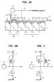
- FIG. 1A A conventional semiconductor input protective device has CMOS semiconductor device, of the kind to which the present invention relates, is shown in Fig. 1A.
- the semiconductor input protective device is constituted by an N-channel MOS transistor M1 having a drain (an N-type diffusion layer 103-1) connected to a signal line 8 which is in turn connected to a pad 9, a source (an N-type diffusion layer 103-2) and a gate electrode 5N both connected to a ground line 6, and a P-channel MOS transistor M2 having a drain (a P-type diffusion layer 102-2) connected to the signal line 8, a source (a P-type diffusion layer 102-1) and a gate electrode 5P both connected to a power source line 7.
- Fig. 1B is an equivalent circuit diagram of the above semiconductor input protective device.
- the MOS semiconductor device used in the above conventional semiconductor input protective device normally has a gate oxide film the thickness of which is the same as that in the MOS semiconductor device of an internal circuit. Therefore, assuming that, for example, the thickness of the gate oxide film is 10 nm, the operating voltage is 3.3 V and the input signal has a TTL (Transistor-Transistor-Logic) level of 5 V, the gate oxide film 11 of the protective MOS semiconductor device will be subjected constantly to an electric field at a maximum of 5.5 MV/cm, thereby allowing the flow of the tunnel current (Fowler-Nordheim current) through the semiconductor device concerned.
- TTL Transistor-Transistor-Logic
- an object of the invention to overcome the problems in the conventional semiconductor input protective device and to provide an improved semiconductor input protective device in which the resistance against surge voltages externally applied to a signal line is effectively enhanced.
- Figs. 2A and 2B are respectively a schematic sectional view and an equivalent circuit diagram thereof showing a semiconductor input protective device not covered by the present invention.
- a lateral NPN bipolar transistor Q and an N-channel Metal-Insulator-Semiconductor (MIS) transistor including, for example, a MOS transistor M3 having as an insulating gate oxide film, a field oxide film 4 of 0.6 ⁇ m thick.
- MIS Metal-Insulator-Semiconductor
- the lateral NPN bipolar transistor Q has an emitter (an N-type diffusion layer 3-4) and a base (the P-type silicon substrate 1) both connected to the ground line 6, and a collector (an N-type diffusion layer 3-3) connected to the signal line 8.
- the N-channel MOS transistor M3 has a source (an N-type diffusion layer 3-1) and a gate electrode 5 both connected to the power source line 7, and a drain (an N-type diffusion layer 3-2) connected to the signal line 8.
- a pad 9 is a bonding terminal formed on the semiconductor chip and is connected to a signal terminal (not shown in the drawings) of the IC package.
- a similar pad is provided correspondingly to the ground terminal GND and the power source terminal V CC in the semiconductor chip.
- the ground line 6, the power source line 7 and the signal line 8, etc. are, for example, aluminum interconnecting layers fabricated in the semiconductor chip.
- the gate electrode 5 of the N-channel MOS transistor M3 is made of the same material as that of the MOS transistor constituting an internal circuit (not shown). Furthermore, the N-type diffusion layers 3-1 to 3-4 are formed simultaneously with the source/drain regions of the N-channel MOS transistors of the internal circuit.
- the lateral NPN bipolar transistor Q When a surge voltage positive with respect to the ground line 6 is applied to the signal line 8 through the pad 9, the lateral NPN bipolar transistor Q operates, thereby releasing the surge voltage to the ground line 6. On the other hand, when a negative surge voltage is applied to the signal line 8, the PN-diode formed by the collector 3-3 and the base (the P-type silicon substrate 1) of this transistor Q is forwardly biased thereby releasing the surge voltage to the ground line 6.
- the gate electrode 5 of the N-channel MOS transistor M3 is connected to the power source line 7 but, this may instead be connected to the signal line 8 as shown by a dotted line in Figs. 2A and 2B.
- N-channel MOS transistors M3 and M4 are connected in parallel between the power source line 7 and the signal line 8 as shown in Fig. 3, with one of the gate electrodes being connected to the power source line 7 and the other being connected to the signal line 8, it is possible to further enhance the effect of the input protection performance.
Description
- The present invention relates to a semiconductor input protective device, and more particularly to a semiconductor input protective device for protecting internal circuits against an abnormal voltage (hereinafter referred to as a "surge voltage") externally applied to a signal line.
- A conventional semiconductor input protective device has CMOS semiconductor device, of the kind to which the present invention relates, is shown in Fig. 1A. As shown therein, the semiconductor input protective device is constituted by an N-channel MOS transistor M1 having a drain (an N-type diffusion layer 103-1) connected to a
signal line 8 which is in turn connected to apad 9, a source (an N-type diffusion layer 103-2) and agate electrode 5N both connected to aground line 6, and a P-channel MOS transistor M2 having a drain (a P-type diffusion layer 102-2) connected to thesignal line 8, a source (a P-type diffusion layer 102-1) and agate electrode 5P both connected to apower source line 7. Fig. 1B is an equivalent circuit diagram of the above semiconductor input protective device. - The above conventional input protective device operates as follows. When a surge voltage positive with respect to the
ground line 6 is applied to thesignal line 8, the surge voltage is released or discharged to theground line 6 by the lateral NPN bipolar action of the N-channel MOS transistor M1 and, when a negative surge voltage is applied to thesignal line 8, a parasitic PN-diode D1 existing between the drain 103-1 of the MOS transistor M1 and a P-type silicon substrate 1 is forwardly biased, so that the surge voltage can be released to theground line 6. - Similarly, when a surge voltage positive with respect to the
power source line 7 is applied to thesignal line 8, a parasitic PN-diode D2 existing between the drain 102-2 of the P-channel MOS transistor M2 and an N-well 10 is forwardly biased, so that the surge voltage can be released to thepower source line 7. On the other hand, when a negative surge voltage is applied to thesignal line 8, the surge voltage can be released to thepower source line 7 due to a drain breakdown of the P-channel MOS transistor M2. - The MOS semiconductor device used in the above conventional semiconductor input protective device normally has a gate oxide film the thickness of which is the same as that in the MOS semiconductor device of an internal circuit. Therefore, assuming that, for example, the thickness of the gate oxide film is 10 nm, the operating voltage is 3.3 V and the input signal has a TTL (Transistor-Transistor-Logic) level of 5 V, the
gate oxide film 11 of the protective MOS semiconductor device will be subjected constantly to an electric field at a maximum of 5.5 MV/cm, thereby allowing the flow of the tunnel current (Fowler-Nordheim current) through the semiconductor device concerned. This state constantly continues during the operation of the semiconductor device, so that the gate oxide film gradually deteriorates, thereby leading eventually to insulation breakdown and to the inability of the MOS semiconductor device to function as a protective device. This is one of the problems in the conventional semiconductor input protective device which is to be solved by the present invention. - The document "Proceedings of the IEEE 1988 CUSTOM INTEGRATED CIRCUITS CONFERENCE, ROCHESTER, MAY 16-19, pages 27.2.1-27.2.4" discloses a resistor less ESD protection device.
- It is, therefore, an object of the invention to overcome the problems in the conventional semiconductor input protective device and to provide an improved semiconductor input protective device in which the resistance against surge voltages externally applied to a signal line is effectively enhanced.
- A semiconductor input protective device according to the present invention is defined in
claim 1. - The above and other objects, features and advantages of the present invention will be apparent from the following description of a preferred embodiment of the invention explained with reference to the accompanying drawings, in which:
- Fig. 1A is a schematic sectional view showing a conventional semiconductor input protective device of the type to which the present invention relates;
- Fig. 1B is an equivalent circuit diagram of the conventional circuit shown in Fig. 1A;
- Fig. 2A is a schematic sectional view showing a semiconductor input protective device not covered by the present invention;
- Fig. 2B is an equivalent circuit diagram of the circuit shown in Fig. 2A; and
- Fig. 3 is an equivalent circuit diagram of a device according to the invention.
- Now, an embodiment not covered by the present invention is explained with reference to the appended drawings in which the same or similar reference symbols or numerals refer to the same or like elements.
- Figs. 2A and 2B are respectively a schematic sectional view and an equivalent circuit diagram thereof showing a semiconductor input protective device not covered by the present invention.
- As shown in the drawings, there are formed on a surface portion of a P-type silicon substrate 1 a lateral NPN bipolar transistor Q and an N-channel Metal-Insulator-Semiconductor (MIS) transistor including, for example, a MOS transistor M3 having as an insulating gate oxide film, a
field oxide film 4 of 0.6 µm thick. - Specifically, the lateral NPN bipolar transistor Q has an emitter (an N-type diffusion layer 3-4) and a base (the P-type silicon substrate 1) both connected to the
ground line 6, and a collector (an N-type diffusion layer 3-3) connected to thesignal line 8. Next, the N-channel MOS transistor M3 has a source (an N-type diffusion layer 3-1) and agate electrode 5 both connected to thepower source line 7, and a drain (an N-type diffusion layer 3-2) connected to thesignal line 8. - In Figs. 2A and 2B, a
pad 9 is a bonding terminal formed on the semiconductor chip and is connected to a signal terminal (not shown in the drawings) of the IC package. A similar pad is provided correspondingly to the ground terminal GND and the power source terminal VCC in the semiconductor chip. Theground line 6, thepower source line 7 and thesignal line 8, etc. are, for example, aluminum interconnecting layers fabricated in the semiconductor chip. Thegate electrode 5 of the N-channel MOS transistor M3 is made of the same material as that of the MOS transistor constituting an internal circuit (not shown). Furthermore, the N-type diffusion layers 3-1 to 3-4 are formed simultaneously with the source/drain regions of the N-channel MOS transistors of the internal circuit. - Hereunder, how the surge voltage externally applied to the semiconductor device is released will be explained.
- When a surge voltage positive with respect to the
ground line 6 is applied to thesignal line 8 through thepad 9, the lateral NPN bipolar transistor Q operates, thereby releasing the surge voltage to theground line 6. On the other hand, when a negative surge voltage is applied to thesignal line 8, the PN-diode formed by the collector 3-3 and the base (the P-type silicon substrate 1) of this transistor Q is forwardly biased thereby releasing the surge voltage to theground line 6. - Similarly, when a surge voltage positive with respect to the
power source line 7 is applied to thesignal line 8, this surge voltage can be released to thepower source line 7 due to the punch-through of the N-channel MOS transistor M3 and, when a negative surge voltage is applied to thesignal line 8, the N-channel MOS transistor M3 becomes conductive and the surge voltage can be released to thepower source line 7 through the MOS transistor M3. - In this embodiment, the
gate electrode 5 of the N-channel MOS transistor M3 is connected to thepower source line 7 but, this may instead be connected to thesignal line 8 as shown by a dotted line in Figs. 2A and 2B. - Furthermore, if two N-channel MOS transistors M3 and M4 are connected in parallel between the
power source line 7 and thesignal line 8 as shown in Fig. 3, with one of the gate electrodes being connected to thepower source line 7 and the other being connected to thesignal line 8, it is possible to further enhance the effect of the input protection performance.
Claims (1)
- A semiconductor input protective device formed between a power source line (7) and a ground line (6) and connected via a signal line (8) to an internal circuit, said semiconductor input protective device comprising:an NPN type bipolar transistor (Q) having a collector (3-3) connected to the signal line (8) extending to a pad (9), and an emitter (3-4) and a base (1) commonly connected to the ground line (6);a first N-channel MIS transistor (M3) in which one of a drain (3-2) and a source (3-1) thereof is connected to said signal line (8) and the other one of the drain and the source is connected to said power source line (7), said first N-channel MIS transistor (M3) having a threshold voltage higher than a power source voltage (VCC) supplied to said power source line (7) and having a gate insulation film (4) thicker than a gate insulation film of a MIS transistor constituting said internal circuit;characterized by
a second N-channel MIS transistor (M4) connected in parallel with said first N-channel MIS transistor (M3), with a gate of one of said first and second N-channel MIS transistors (M3, M4) being connected to the signal line (8) and a gate of the other one of said first and second N-channel MIS transistors being connected to the power source line (7).
Applications Claiming Priority (2)
| Application Number | Priority Date | Filing Date | Title |
|---|---|---|---|
| JP3279522A JPH05121670A (en) | 1991-10-25 | 1991-10-25 | Semiconductor input protective device |
| JP279522/91 | 1991-10-25 |
Publications (2)
| Publication Number | Publication Date |
|---|---|
| EP0538752A1 EP0538752A1 (en) | 1993-04-28 |
| EP0538752B1 true EP0538752B1 (en) | 1997-03-26 |
Family
ID=17612200
Family Applications (1)
| Application Number | Title | Priority Date | Filing Date |
|---|---|---|---|
| EP92117752A Expired - Lifetime EP0538752B1 (en) | 1991-10-25 | 1992-10-16 | Semiconductor input protective device against external surge voltage |
Country Status (4)
| Country | Link |
|---|---|
| US (1) | US5349227A (en) |
| EP (1) | EP0538752B1 (en) |
| JP (1) | JPH05121670A (en) |
| DE (1) | DE69218543T2 (en) |
Families Citing this family (12)
| Publication number | Priority date | Publication date | Assignee | Title |
|---|---|---|---|---|
| KR100291540B1 (en) * | 1992-10-29 | 2001-09-17 | 사와무라 시코 | Input / output protection circuit |
| JPH06332011A (en) * | 1993-05-18 | 1994-12-02 | Sony Corp | Semiconductor integrated substrate and semiconductor device |
| US5607867A (en) * | 1994-07-15 | 1997-03-04 | Texas Instruments Incorporated | Method of forming a controlled low collector breakdown voltage transistor for ESD protection circuits |
| JPH0951078A (en) * | 1995-05-29 | 1997-02-18 | Mitsubishi Electric Corp | Semiconductor memory and semiconductor device |
| JPH08330605A (en) * | 1995-05-31 | 1996-12-13 | Nec Yamagata Ltd | Semiconductor device |
| KR100194669B1 (en) * | 1995-12-20 | 1999-06-15 | 윤종용 | Input Protection Circuits and Protection Devices |
| TW320772B (en) * | 1996-09-23 | 1997-11-21 | United Microelectronics Corp | Protection component and production method for low voltage static discharge |
| JP4330183B2 (en) * | 1997-09-30 | 2009-09-16 | 株式会社ルネサステクノロジ | Semiconductor memory device |
| JP3617425B2 (en) | 2000-07-28 | 2005-02-02 | 株式会社デンソー | Input interface circuit of semiconductor integrated circuit device |
| KR100482370B1 (en) * | 2002-09-27 | 2005-04-13 | 삼성전자주식회사 | Semiconductor device having difference thickness of gate oxide |
| JP2008205271A (en) * | 2007-02-21 | 2008-09-04 | Matsushita Electric Ind Co Ltd | Semiconductor protection circuit, manufacturing method thereof, and operation method thereof |
| US9331097B2 (en) * | 2014-03-03 | 2016-05-03 | International Business Machines Corporation | High speed bipolar junction transistor for high voltage applications |
Family Cites Families (12)
| Publication number | Priority date | Publication date | Assignee | Title |
|---|---|---|---|---|
| JPS5598867A (en) * | 1979-01-19 | 1980-07-28 | Mitsubishi Electric Corp | Protecting device |
| JPS5755552A (en) * | 1980-09-19 | 1982-04-02 | Matsushita Electric Ind Co Ltd | Electromagnetic actuating device of tape recorder |
| JPS57109375A (en) * | 1980-12-26 | 1982-07-07 | Fujitsu Ltd | Mis type transistor protection circuit |
| JPS59231847A (en) * | 1983-06-15 | 1984-12-26 | Hitachi Micro Comput Eng Ltd | Semiconductor integrated circuit device |
| JPS6053070A (en) * | 1983-09-02 | 1985-03-26 | Nec Corp | Mos-fet integrated circuit device |
| US4692781B2 (en) * | 1984-06-06 | 1998-01-20 | Texas Instruments Inc | Semiconductor device with electrostatic discharge protection |
| JPS6115373A (en) * | 1984-07-02 | 1986-01-23 | Rohm Co Ltd | Semiconductor device |
| JPS6269678A (en) * | 1985-09-24 | 1987-03-30 | Toshiba Corp | Input protective circuit |
| JPS63305545A (en) * | 1987-06-05 | 1988-12-13 | Hitachi Ltd | Semiconductor integrated circuit device |
| US4930037A (en) * | 1989-02-16 | 1990-05-29 | Advaced Micro Devices, Inc. | Input voltage protection system |
| JP2504838B2 (en) * | 1989-07-27 | 1996-06-05 | 日本電気アイシーマイコンシステム株式会社 | Input / output protection device for semiconductor integrated circuit |
| JPH03196677A (en) * | 1989-12-26 | 1991-08-28 | Nec Corp | Semiconductor device |
-
1991
- 1991-10-25 JP JP3279522A patent/JPH05121670A/en active Pending
-
1992
- 1992-10-15 US US07/961,863 patent/US5349227A/en not_active Expired - Fee Related
- 1992-10-16 DE DE69218543T patent/DE69218543T2/en not_active Expired - Fee Related
- 1992-10-16 EP EP92117752A patent/EP0538752B1/en not_active Expired - Lifetime
Non-Patent Citations (1)
| Title |
|---|
| Proceedings of the IEEE 1988 Custom Integrated Circuits Conference, Rochester, May 16-19, pages 27.2.1-27.2.4 * |
Also Published As
| Publication number | Publication date |
|---|---|
| JPH05121670A (en) | 1993-05-18 |
| EP0538752A1 (en) | 1993-04-28 |
| US5349227A (en) | 1994-09-20 |
| DE69218543T2 (en) | 1997-10-23 |
| DE69218543D1 (en) | 1997-04-30 |
Similar Documents
| Publication | Publication Date | Title |
|---|---|---|
| US6861680B2 (en) | Silicon-on-insulator diodes and ESD protection circuits | |
| US5060037A (en) | Output buffer with enhanced electrostatic discharge protection | |
| EP0575062B1 (en) | ESD protection of output buffers | |
| US5903420A (en) | Electrostatic discharge protecting circuit having a plurality of current paths in both directions | |
| JP2815561B2 (en) | CMOS electrostatic discharge protection circuit using low voltage triggered silicon controlled rectifier | |
| KR0164908B1 (en) | Semiconductor device having a protective transistor | |
| JP4856803B2 (en) | Lateral bipolar device with substrate-triggered electrostatic breakdown protection or electrical overstress protection | |
| US6479872B1 (en) | Dynamic substrate-coupled electrostatic discharging protection circuit | |
| EP0324185B1 (en) | Input protecting circuit in use with a MOS semiconductor device | |
| US5751042A (en) | Internal ESD protection circuit for semiconductor devices | |
| KR20020011894A (en) | Semiconductor device | |
| US4609931A (en) | Input protection MOS semiconductor device with zener breakdown mechanism | |
| EP0573213A1 (en) | ESD protection of output buffers | |
| EP0538752B1 (en) | Semiconductor input protective device against external surge voltage | |
| US5604655A (en) | Semiconductor protection circuit and semiconductor protection device | |
| JPH10340996A (en) | Protection circuit | |
| US7217980B2 (en) | CMOS silicon-control-rectifier (SCR) structure for electrostatic discharge (ESD) protection | |
| US6323522B1 (en) | Silicon on insulator thick oxide structure and process of manufacture | |
| US5710452A (en) | Semiconductor device having electrostatic breakdown protection circuit | |
| JP3320872B2 (en) | CMOS integrated circuit device | |
| JP3345296B2 (en) | Protection circuit and circuit for semiconductor element on insulator | |
| US20030043517A1 (en) | Electro-static discharge protecting circuit | |
| US6707653B2 (en) | Semiconductor controlled rectifier for use in electrostatic discharge protection circuit | |
| US6894320B2 (en) | Input protection circuit | |
| JPH06236965A (en) | Semiconductor device |
Legal Events
| Date | Code | Title | Description |
|---|---|---|---|
| PUAI | Public reference made under article 153(3) epc to a published international application that has entered the european phase |
Free format text: ORIGINAL CODE: 0009012 |
|
| 17P | Request for examination filed |
Effective date: 19930118 |
|
| AK | Designated contracting states |
Kind code of ref document: A1 Designated state(s): DE FR GB |
|
| 17Q | First examination report despatched |
Effective date: 19950829 |
|
| GRAG | Despatch of communication of intention to grant |
Free format text: ORIGINAL CODE: EPIDOS AGRA |
|
| GRAH | Despatch of communication of intention to grant a patent |
Free format text: ORIGINAL CODE: EPIDOS IGRA |
|
| GRAH | Despatch of communication of intention to grant a patent |
Free format text: ORIGINAL CODE: EPIDOS IGRA |
|
| GRAA | (expected) grant |
Free format text: ORIGINAL CODE: 0009210 |
|
| AK | Designated contracting states |
Kind code of ref document: B1 Designated state(s): DE FR GB |
|
| REF | Corresponds to: |
Ref document number: 69218543 Country of ref document: DE Date of ref document: 19970430 |
|
| ET | Fr: translation filed | ||
| PLBE | No opposition filed within time limit |
Free format text: ORIGINAL CODE: 0009261 |
|
| STAA | Information on the status of an ep patent application or granted ep patent |
Free format text: STATUS: NO OPPOSITION FILED WITHIN TIME LIMIT |
|
| 26N | No opposition filed | ||
| PGFP | Annual fee paid to national office [announced via postgrant information from national office to epo] |
Ref country code: FR Payment date: 20011010 Year of fee payment: 10 |
|
| PGFP | Annual fee paid to national office [announced via postgrant information from national office to epo] |
Ref country code: GB Payment date: 20011017 Year of fee payment: 10 |
|
| PGFP | Annual fee paid to national office [announced via postgrant information from national office to epo] |
Ref country code: DE Payment date: 20011029 Year of fee payment: 10 |
|
| REG | Reference to a national code |
Ref country code: GB Ref legal event code: IF02 |
|
| PG25 | Lapsed in a contracting state [announced via postgrant information from national office to epo] |
Ref country code: GB Free format text: LAPSE BECAUSE OF NON-PAYMENT OF DUE FEES Effective date: 20021016 |
|
| PG25 | Lapsed in a contracting state [announced via postgrant information from national office to epo] |
Ref country code: DE Free format text: LAPSE BECAUSE OF NON-PAYMENT OF DUE FEES Effective date: 20030501 |
|
| GBPC | Gb: european patent ceased through non-payment of renewal fee |
Effective date: 20021016 |
|
| PG25 | Lapsed in a contracting state [announced via postgrant information from national office to epo] |
Ref country code: FR Free format text: LAPSE BECAUSE OF NON-PAYMENT OF DUE FEES Effective date: 20030630 |
|
| REG | Reference to a national code |
Ref country code: FR Ref legal event code: ST |