JP4330183B2 - Semiconductor memory device - Google Patents
Semiconductor memory device Download PDFInfo
- Publication number
- JP4330183B2 JP4330183B2 JP26605797A JP26605797A JP4330183B2 JP 4330183 B2 JP4330183 B2 JP 4330183B2 JP 26605797 A JP26605797 A JP 26605797A JP 26605797 A JP26605797 A JP 26605797A JP 4330183 B2 JP4330183 B2 JP 4330183B2
- Authority
- JP
- Japan
- Prior art keywords
- potential
- power supply
- type
- well region
- memory cell
- Prior art date
- Legal status (The legal status is an assumption and is not a legal conclusion. Google has not performed a legal analysis and makes no representation as to the accuracy of the status listed.)
- Expired - Fee Related
Links
Images


Classifications
-
- G—PHYSICS
- G11—INFORMATION STORAGE
- G11C—STATIC STORES
- G11C11/00—Digital stores characterised by the use of particular electric or magnetic storage elements; Storage elements therefor
- G11C11/21—Digital stores characterised by the use of particular electric or magnetic storage elements; Storage elements therefor using electric elements
- G11C11/34—Digital stores characterised by the use of particular electric or magnetic storage elements; Storage elements therefor using electric elements using semiconductor devices
- G11C11/40—Digital stores characterised by the use of particular electric or magnetic storage elements; Storage elements therefor using electric elements using semiconductor devices using transistors
- G11C11/401—Digital stores characterised by the use of particular electric or magnetic storage elements; Storage elements therefor using electric elements using semiconductor devices using transistors forming cells needing refreshing or charge regeneration, i.e. dynamic cells
- G11C11/4063—Auxiliary circuits, e.g. for addressing, decoding, driving, writing, sensing or timing
- G11C11/407—Auxiliary circuits, e.g. for addressing, decoding, driving, writing, sensing or timing for memory cells of the field-effect type
-
- H—ELECTRICITY
- H01—ELECTRIC ELEMENTS
- H01L—SEMICONDUCTOR DEVICES NOT COVERED BY CLASS H10
- H01L27/00—Devices consisting of a plurality of semiconductor or other solid-state components formed in or on a common substrate
- H01L27/02—Devices consisting of a plurality of semiconductor or other solid-state components formed in or on a common substrate including semiconductor components specially adapted for rectifying, oscillating, amplifying or switching and having at least one potential-jump barrier or surface barrier; including integrated passive circuit elements with at least one potential-jump barrier or surface barrier
- H01L27/04—Devices consisting of a plurality of semiconductor or other solid-state components formed in or on a common substrate including semiconductor components specially adapted for rectifying, oscillating, amplifying or switching and having at least one potential-jump barrier or surface barrier; including integrated passive circuit elements with at least one potential-jump barrier or surface barrier the substrate being a semiconductor body
- H01L27/08—Devices consisting of a plurality of semiconductor or other solid-state components formed in or on a common substrate including semiconductor components specially adapted for rectifying, oscillating, amplifying or switching and having at least one potential-jump barrier or surface barrier; including integrated passive circuit elements with at least one potential-jump barrier or surface barrier the substrate being a semiconductor body including only semiconductor components of a single kind
- H01L27/085—Devices consisting of a plurality of semiconductor or other solid-state components formed in or on a common substrate including semiconductor components specially adapted for rectifying, oscillating, amplifying or switching and having at least one potential-jump barrier or surface barrier; including integrated passive circuit elements with at least one potential-jump barrier or surface barrier the substrate being a semiconductor body including only semiconductor components of a single kind including field-effect components only
- H01L27/088—Devices consisting of a plurality of semiconductor or other solid-state components formed in or on a common substrate including semiconductor components specially adapted for rectifying, oscillating, amplifying or switching and having at least one potential-jump barrier or surface barrier; including integrated passive circuit elements with at least one potential-jump barrier or surface barrier the substrate being a semiconductor body including only semiconductor components of a single kind including field-effect components only the components being field-effect transistors with insulated gate
- H01L27/092—Devices consisting of a plurality of semiconductor or other solid-state components formed in or on a common substrate including semiconductor components specially adapted for rectifying, oscillating, amplifying or switching and having at least one potential-jump barrier or surface barrier; including integrated passive circuit elements with at least one potential-jump barrier or surface barrier the substrate being a semiconductor body including only semiconductor components of a single kind including field-effect components only the components being field-effect transistors with insulated gate complementary MIS field-effect transistors
- H01L27/0928—Devices consisting of a plurality of semiconductor or other solid-state components formed in or on a common substrate including semiconductor components specially adapted for rectifying, oscillating, amplifying or switching and having at least one potential-jump barrier or surface barrier; including integrated passive circuit elements with at least one potential-jump barrier or surface barrier the substrate being a semiconductor body including only semiconductor components of a single kind including field-effect components only the components being field-effect transistors with insulated gate complementary MIS field-effect transistors comprising both N- and P- wells in the substrate, e.g. twin-tub
Description
【0001】
【発明の属する技術分野】
この発明は、半導体記憶装置に関し、より特定的には、高速に外部から与えられる信号に応じて、動作することが可能な半導体記憶装置の構成に関する。
【0002】
【従来の技術】
半導体記憶装置を高速に動作させるためには、外部から半導体記憶装置に入力される信号の立上がりおよび立下がりを急峻に変化させる必要が生じる。
【0003】
このために、半導体記憶装置にデータを与える外部の装置の信号ドライバ回路の駆動力は高く設定されることになる。
【0004】
しかしながら、実際に半導体記憶装置が実装されているボード上の配線には、たとえば、等価的にインダクタンス成分が分布定数として寄生している。このため、入力信号の時間変化率が大きいほど半導体記憶装置に取込まれる信号波形の乱れが大きくなる。
【0005】
図12は、半導体記憶装置内部での入力信号波形の時間変化を示す図である。図中入力信号の“H”レベルは、電位VIHのレベルであるものとし、入力信号の“L”レベルは、電位VILのレベルを有するものとする。
【0006】
時刻t1において、入力信号が“L”レベルから“H”レベルに向かって立上がり始めたとする。この場合、上述したように、半導体記憶装置内部に取込まれる信号波形は、電位レベルVIHを超えていわゆるオーバーシュートする波形となる。
【0007】
同様にして、時刻t2においては、入力信号が“H”レベルから“L”レベルへ立下がるものとする。このときも、ボード上の配線に存在する寄生インダクタンス成分により、入力信号波形にはアンダーシュートが存在することになる。
【0008】
しかしながら、このようなオーバーシュートやアンダーシュートが入力信号波形に存在すると、半導体記憶装置の動作の不安定化をもたらし、この半導体記憶装置が実装されているボード上に構成されるシステム自体の動作の安定性も損なわれることになる。
【0009】
したがって、一般には半導体記憶装置の側において、入力信号波形を整形して、入力信号のオーバーシュートやアンダーシュートの発生を抑制することが行なわれる。
【0010】
図13は、半導体記憶装置にオンチップ内蔵される、入力波形を整形するためのクランプ回路700の構成を示す回路図である。
【0011】
図13を参照して、入力パッド702に与えられた信号を伝達する信号配線704には、電源電位Vddとの間に、NチャネルMOSトランジスタQ1が設けられる。信号配線704と接地電位GNDとの間には、さらにNチャネルMOSトランジスタQ2が設けられる。NチャネルMOSトランジスタQ1のゲートは、信号配線704と接続され、信号配線704から、電源電位Vddに向かう方向が順方向となるようにダイオード接続されている。
【0012】
同様にして、NチャネルMOSトランジスタQ2のゲートは、接地電位GNDと結合し、この接地電位GNDから信号配線704に向かう方向が順方向となるようにダイオード接続されている。
【0013】
図14は、図13に示したクランプ回路700の断面構造を説明するための断面図である。
【0014】
NチャネルMOSトランジスタQ1およびQ2は、ともに、P型基板720の主表面側に形成されたP型ウェル722中に設けられる構成となっている。
【0015】
P型ウェル722は、たとえば、外部電源電位と接地電位とを受けて、負電圧の基板電位を発生する基板電位発生回路(図示せず)から供給される基板電位Vbbにバイアスされている。
【0016】
図13および図14に示したようなクランプ素子700の構成では、入力信号のレベルは、電位Vdd+Vth(VthはNチャネルMOSトランジスタQ1のしきい値電圧)より高くなると、NチャネルMOSトランジスタQ1が導通状態となる。
【0017】
このとき、NチャネルMOSトランジスタQ1のバックバイアスが電位Vbbであるため、クランプ動作が行なわれる際には、NチャネルMOSトランジスタQ1のソース基板間電位Vsbは、Vsb=Vdd+|Vbb|となる。このため、NチャネルMOSトランジスタは、大きな基板効果を受けることになる。ここで、|Vbb|は、基板電位Vbbの絶対値である。
【0018】
したがって、通常の基板バイアス状態で、NチャネルMOSトランジスタのしきい値電圧Vth=0.8Vであるとすると、このしきい値電圧は、大きな基板効果により、たとえば、Vth=1.2V程度まで上昇する。
【0019】
このため、図13および図14に示したようなクランプ回路700の構成では、クランプ効果が有効に働かないという欠点がある。
【0020】
また、図13および図14に示した構成では、入力サージに対しても耐性が悪いという欠点がある。これは、クランプ素子がともにNチャネルMOSトランジスタで形成されているため、入力サージに対して、NチャネルMOSトランジスタの酸化膜破壊が起こってしまうためである。このため、図13および図14に示したようなクランプ回路700の構成は、実際に使用されるデバイスに用いるには困難がある。
【0021】
図15は、半導体記憶装置にオンチップ内蔵される、クランプ回路の他の例のクランプ回路800の構成を示す回路図である。
【0022】
クランプ回路800においては、信号配線704と電源電位Vddとの間には、PチャネルMOSトランジスタQ3が設けられる。
【0023】
PチャネルMOSトランジスタQ3のゲートは、電源電位Vddと結合し、したがって、この信号配線704から電源電位Vddに向かう方向が順方向となるようにダイオード接続されている。
【0024】
その他の点は、図13に示したクランプ回路700の構成と同様であるので、同一部分には同一符号を付してその説明は繰返さない。
【0025】
図16は、図15に示したクランプ回路800の断面構造を説明するための断面図である。
【0026】
P型基板720の主表面側に形成されるN型ウェル820中にPチャネルMOSトランジスタQ3が設けられ、N型ウェル820に隣接して設けられるP型ウェル822中に、NチャネルMOSトランジスタQ2が設けられる構成となっている。
【0027】
N型ウェル820は、電源電位Vddにバイアスされ、P型ウェル822は、接地電位GNDにバイアスされている。
【0028】
このとき、P型基板720は、接地電位にバイアスされている必要がある。
それは、以下に説明するような理由による。
【0029】
すなわち、図16に示したクランプ回路800の構成においては、入力信号の電位レベルが、Vdd+Vbi(電位VbiはPN接合の順方向立上がり電圧)以上になると、入力信号配線が接続された、PチャネルMOSトランジスタQ3のドレイン領域に対応するP型拡散領域824とN型ウェル820とが順方向にバイアスされる。さらに、基板がP型であるため、P型拡散領域824、N型ウェル820およびP基板720とにより構成されるPNPバイポーラトランジスタがターンオンする。
【0030】
このようにして、クランプ電流は、P型拡散領域824からP型基板へ流れることになる。したがって、たとえばP基板720に基板電位発生回路(図示せず)から電位が供給されていると、この基板電位発生回路に対して、クランプ電流が流入してしまうことになる。
【0031】
このようなクランプ電流のが、基板中に流入すると、基板が正電位となってしまう。このことは、CMOS回路のラッチアップ現象を誘発することとなり、DRAMの正常動作にとっては致命的である。
【0032】
したがって、P基板720は接地電位GNDにバイアスされている必要がある。
【0033】
一方で、クランプ素子として動作する場合、PN接合は、MOSトランジスタよりも電流吸収能力が大きいという利点がある。
【0034】
したがって、図13に示したクランプ回路700よりも、クランプ回路800の構成の方が入力信号のオーバーシュートを抑制するという点では望ましい構成といえる。
【0035】
図17は、半導体記憶装置にオンチップ実装されるクランプ回路のさらに他の例のクランプ回路900の構成を示す回路図である。
【0036】
クランプ回路900においては、入力信号配線704から電源電位Vddとの間には、信号配線704から電源電位Vddへ向かう方向が順方向となるようなPN接合ダイオードQ4が接続され、接地電位GNDと入力信号配線704との間には、接地電位GNDから入力信号配線704へ向かう方向が順方向となるように、PN接合ダイオードQ5が接続されている。
【0037】
図18は、図17に示したクランプ回路900の断面構造を説明するための断面図である。
【0038】
図18においては、P型基板720の主表面側に形成されるNウェル820には、電源電位Vddが供給されている。
【0039】
一方、Nウェル920に隣接して設けられるPウェル922には、接地電位GNDが供給されている。
【0040】
入力信号配線704は、N型ウェル920の主表面側に設けられるP型拡散領域924と接続し、また、入力信号配線704は、P型ウェル922の主表面側に形成されるN型拡散領域926とも接続している。
【0041】
このような構成とすることで、図16において説明したクランプ回路800と同様に、入力信号の電位レベルが電位Vdd+Vbi以上になると、信号配線と接続するP型拡散領域924とNウェル920とが順方向にバイアスされることになる。この場合も、基板がP型であるため、P型拡散領域924、Nウェル920およびP型基板720により構成されるPNPバイポーラトランジスタがターンオンすることになる。
【0042】
したがって、図16の場合と同様に、クランプ電流は、P型拡散領域924からP型基板720へと流れる。つまり、図18に示したクランプ回路900においても、P型基板は接地電位GNDに接続していなければならない。
【0043】
この場合、クランプ素子がPN接合ダイオードであるため、MOSトランジスタを用いる場合よりも電流吸収能力が大きい。さらに、PN接合ダイオードを用いた場合は、クランプ素子中に酸化膜が存在しないため、入力サージによって酸化膜が破壊されることがないという利点もある。
【0044】
したがって、クランプ回路をPN接合ダイオードを用いることにより構成することの利点は大きい。
【0045】
【発明が解決しようとする課題】
図19は、半導体記憶装置、特にダイナミック型ランダムアクセスメモリ(以下、DRAMと呼ぶ)におけるメモリセルアレイ部の断面構造を示す図であり、図20は、メモリセルアレイの構成を示す平面図である。
【0046】
図19を参照して、まず、P型基板720の主表面には、P型ウェル740が設けられる。このP型ウェル740中に、メモリセルが配置される。
【0047】
一般に、各メモリセルは、1つのNチャネルMOSトランジスタ750と、1つのメモリセルキャパシタ(図示せず)により構成される。
【0048】
ここで、NチャネルMOSトランジスタ750は、メモリセルキャパシタの一方電極と、選択されたビット線対との接続を開閉するためのトランジスタであり、アクセストランジスタと呼ばれる。
【0049】
P型ウェル740は、アクセストランジスタのしきい値電圧を高め、メモリセルに蓄積された電荷の保持時間を長くするため、接地電位よりも低い負の電圧Vbbに固定されている。
【0050】
また、P型ウェル740内には、メモリセルから読出されるデータに応じて、選択されたメモリセルに接続するビット線対の電位レベルを増幅するためのN型MOSセンスアンプ752も設けられている。
【0051】
P型ウェル740に近接して、N型ウェル742が設けられる。このN型ウェル742領域には、上述したNチャネル型MOSセンスアンプ752とともに、選択されたメモリセル中の記憶データに応じて、ビット線対の電位レベルを増幅するためのPチャネルMOS型センスアンプ754が設けられている。N型ウェル742の電位レベルは、PチャネルMOS型センスアンプの電源電位Vccに固定されている。ここで、電源電位Vccは、外部電源電圧Vddを半導体記憶装置中に搭載された降圧回路(図示せず)により降圧された内部電源電位を表わすものとする。
【0052】
さらに、P型ウェル740に近接して、もう1つのN型ウェル744が設けられる。このN型ウェル744には、選択されたワード線の電位レベルを駆動するためのワードドライバ回路を構成するトランジスタのうち、Pチャネル型MOSトランジスタ756が形成されている。ワード線を駆動するワードドライバが出力する“H”レベルは、アクセストランジスタによる電圧降下の影響を避けるために、一般には、内部電源電圧Vccよりも高い電圧Vppのレベルが用いられる。この電圧Vppは、半導体集積回路装置中に搭載される昇圧回路により、外部電源電圧Vddより生成される。
【0053】
このN型ウェル744は、したがって、この電位Vppの電位レベルに固定されている。
【0054】
次に、図20を参照して、メモリセルアレイは、複数のメモリセルブロックに分割され、各メモリセルブロックに対応して、センスアンプ帯SABが配置されている。さらに、メモリセルブロックの各々に対応して、図19に示したワードドライバ回路が設けられるワードドライバ帯WDBが、センスアンプ帯とは交差する方向に設けられている。
【0055】
図21は、従来用いられてきたDRAMのメモリセルアレイ構成の別の例を示す断面図である。
【0056】
図21に示したメモリセルアレイにおいても、その平面構成は、図20に示したメモリセルアレイの構成と同様であるものとする。
【0057】
図21に示した構成においても、P型基板720の主表面側に形成されたP型ウェル740内に、メモリセルに含まれるNチャネル型MOSトランジスタ750と、センスアンプを構成するNチャネルMOSセンスアンプ752とが設けられ、さらに、ワードドライバを構成するNチャネルMOSトランジスタ758も設けられる構成となっている。
【0058】
このP型ウェル740は、アクセストランジスタのしきい値電圧を高め、メモリセルに蓄積された電荷の保持時間を長くするため、接地電位GNDよりも低い負の電圧Vbbに固定されている。
【0059】
また、P型ウェル740に隣接して、N型ウェル742が設けられる。N型ウェル742中には、センスアンプを構成するPチャネルMOSセンスアンプ754が設けられる。N型ウェル742の電位レベルは、内部電源電圧Vccに固定されている。
【0060】
ここで、図21に示した構成は、図19に示した構成に比べて、ワード線を駆動するワードドライバ回路は、Nチャネル型MOSトランジスタ758のみで構成されている点で異なる。
【0061】
したがって、図21に示した構成においては、ワードドライバには、いわゆる、セルフブーストタイプの回路を用いる構成となっている。
【0062】
このため、図21に示した構成では、ワード線の電位レベルを駆動するにあたり、ワードドライバ回路は、プリチャージ動作を行なってからブースト動作を行なうという順序シーケンスが必要である。
【0063】
したがって、ワード線を活性化するのに図19に示した構成に比べると時間が余計にかかり、アクセス速度が遅れてしまうという欠点がある。
【0064】
ここで、図19においても図21においても、P型基板の電位レベルは、P型ウェルの電位レベル、すなわち、基板電位Vbbに保持されている。
【0065】
したがって、図19や図21に示したような構成を有するDRAMに対して、図15から図18において示したクランプ回路800および900を用いようとすると、以下に説明するような問題点が存在する。
【0066】
すなわち、図15に示したクランプ回路800においても、図17において示したクランプ回路900においても、P型基板の電位レベルは接地電位GNDであることが必要である。
【0067】
これに対して、図19に示した構成においても、図21に示した構成においても、P型基板の電位レベルは基板電位Vbbでなければならない。したがって、クランプ回路800および900をそのまま、図19または図21に示したDRAMに適用することはできない。
【0068】
このような問題点を解決するために、図22に示したような、断面構造を有するDRAMの構成を用いることが可能である。
【0069】
すなわち、図22に示したDRAMの断面構造においては、図19に示したDRAMの断面構造と、以下の点が異なる。
【0070】
すなわち、図22に示したDRAMの構成においては、P型ウェル740が、トリプルN型ウェル746を導入することで、P型基板720と電気的に分離される構成となっている。
【0071】
すなわち、図22に示したような構成とすることで、P型ウェル740の電位レベルは基板電位Vbbに保持し、N型ウェル744の電位レベルは昇圧電位Vppに保持し、かつP型基板の電位レベルは接地電位とすることが可能となる。
【0072】
しかしながら、図22に示したような構成では、以下に説明するような問題点がある。
【0073】
すなわち、図22に示した構成では、P型ウェル740をN型のウェルが完全に取囲む構成とするために、P型ウェル740とN型ウェル742との間の領域にも、P型ウェル740に近接して、N型ウェル748が設けられる必要がある。
【0074】
このとき、N型ウェル744、トリプルN型ウェル746およびN型ウェル748は、完全にP型ウェル740を取囲み、かつ、その電位レベルは昇圧電位Vppに保持されることになる。
【0075】
一方、PチャネルMOSセンスアンプ754が設けられるN型ウェル742は、電位レベルが内部電源電位Vccに保持される必要があるため、N型ウェル748とN型ウェル742との間には、分離帯780を設ける必要がある。
【0076】
このような分離帯を設けることは、図20に示すように、メモリセルアレイ中にセンスアンプ帯が複数個設けられる構成となっている場合には、メモリセルアレイ面積の増大をもたらし、ひいては、チップ面積の増大を招いてしまう。
【0077】
P型ウェル740の電位レベルを基板電位Vbbとしつつ、かつP型基板の電位レベルを接地電位GNDとするためには、たとえばトリプルN型ウェル746の電位レベルをVccに固定するという方法もある。
【0078】
この場合は、P型ウェル740は、トリプルウェル746とN型ウェル748と、さらに、N型ウェル744とP型ウェル740との間に設けられる新たなN型ウェルにより完全に取囲まれることで、P型基板と電気的に分離される必要がある。
【0079】
この場合は、ワードドライバを構成するPチャネルMOSトランジスタ756が形成されるN型ウェル744とこのP型ウェル740を取囲むために設けられた新たなN型ウェルとの間に分離帯が必要となる。
【0080】
したがって、この場合も、図20に示すように、ワードドライバがメモリセルアレイ中に複数個設けられる構成となっている場合、メモリセルアレイの面積の増大、ひいてはチップ面積の増大を招いてしまう。
【0081】
この発明は、上記のような問題点を解決するためになされたものであって、その目的は、PN接合を用いたクランプ回路を搭載することが可能なDRAMを提供することである。
【0082】
この発明のさらに他の目的は、PN接合を用いたクランプ回路を搭載した場合でも、チップ面積の増大を抑制することが可能なDRAMを提供することである。
【0083】
【課題を解決するための手段】
請求項1記載の半導体記憶装置は、P型の半導体基板上に形成される半導体記憶装置であって、外部からの信号を受ける入力パッドと、第1の電源電位を受ける第1の電源パッドと、第1の電源電位よりも高い第2の電源電位を受ける第2の電源パッドと、第1の電源電位および第2の電源電位を受けて、負電位の基板電位を生成し、半導体基板に供給する基板電位生成手段と、入力パッドに与えられた信号を伝達する入力信号配線と、半導体基板の主表面に形成され、入力信号配線の電位レベルを受けるN型の第1のウェル領域と、第1のウェル領域内に、第1のウェル領域に主表面以外を取囲まれるように形成され、入力信号配線の電位レベルを受けるP型の第2のウェル領域と、第2のウェル領域の主表面側に形成され、第2の電源電位を受けるN型の第1の不純物ドーピング領域とを備える。
【0084】
請求項2記載の半導体記憶装置は、請求項1記載の半導体記憶装置の構成に加えて、第1および第2の電源電位を受けて、第1および第2の電源電位の中間の値を有する内部電源電位を発生する降圧手段と、入力信号配線に与えられた信号に応じて、書込まれたデータを保持する内部回路をさらに備え、内部回路は、半導体基板の主表面に形成されるP型の第3のウェル領域と、半導体基板の主表面に第3のウェル領域に隣接して形成され、内部電源電位が供給されるN型の第4のウェル領域と、第3のウェル領域に形成されるメモリセルアレイとを含み、メモリセルアレイは、メモリセルアレイの行方向に配置される複数のワード線と、メモリセルアレイの列方向に配置される複数のビット線対と、ワード線とビット線対との交点に配置されるメモリセルと、読出動作において、ビット線対の電位差を選択されたメモリセルに保持されるデータに応じて、増幅するN型チャネルセンスアンプとを有し、第4のウェル領域に形成され、読出動作において、ビット線対の電位差を選択されたメモリセルに保持されるデータに応じて、増幅するP型チャネルセンスアンプとを含む。
【0085】
請求項3記載の半導体記憶装置は、P型の半導体基板上に形成される半導体記憶装置であって、外部からの信号を受ける入力パッドと、第1の電源電位を受ける第1の電源パッドと、第1の電源電位よりも第2の電源電位を受ける第2の電源パッドと、第1の電源電位および第2の電源電位とを受けて、負電位の基板電位を生成し、半導体基板に供給する基板電位生成手段と、入力パッドに与えられた信号を伝達する入力信号配線と、半導体基板の主表面に形成され、所定の電位を受けるN型の第1のウェル領域と、第1のウェル領域内に、第1のウェル領域に主表面以外を取囲まれるように形成され、第1の電源電位を受けるP型の第2のウェル領域と、第2のウェル領域の主表面側に形成され、入力信号配線の電位レベルを受けるN型の第2の不純物ドーピング領域とを備える。
【0086】
請求項4記載の半導体記憶装置は、請求項3記載の半導体記憶装置の構成において、所定の電位は、第1の電源電位である。
【0087】
請求項5記載の半導体記憶装置は、請求項3記載の半導体記憶装置の構成において、所定の電位は、第2の電源電位である。
【0088】
請求項6記載の半導体記憶装置は、請求項3記載の半導体記憶装置の構成に加えて、第1および第2の電源電位を受けて、第1および第2の電源電位の中間の値を有する内部電源電位を発生する降圧手段と、入力信号配線に与えられた信号に応じて、書込まれたデータを保持する内部回路をさらに備え、内部回路は、半導体基板の主表面に形成されるP型の第3のウェル領域と、半導体基板の主表面に第3のウェル領域に隣接して形成され、内部電源電位が供給されるN型の第4のウェル領域と、第3のウェル領域に形成されるメモリセルアレイとを含み、メモリセルアレイは、メモリセルアレイの行方向に配置される複数のワード線と、メモリセルアレイの列方向に配置される複数のビット線対と、ワード線とビット線対との交点に配置されるメモリセルと、読出動作において、ビット線対の電位差を選択されたメモリセルに保持されるデータに応じて、増幅するN型チャネルセンスアンプとを有し、第4のウェル領域に形成され、読出動作において、ビット線対の電位差を選択されたメモリセルに保持されるデータに応じて、増幅するP型チャネルセンスアンプとを含む。
【0089】
【発明の実施の形態】
[実施の形態1]
図1は、本発明の実施の形態1の半導体記憶装置1000の構成を示す概略ブロック図である。
【0090】
図1を参照して、半導体記憶装置1000は、長辺方向および短辺方向にそれぞれ沿って存在する中央領域CR1およびCR2により互いに分離される4つのメモリセルプレーンM♯0〜M♯3を含む。
【0091】
メモリセルプレーンM♯0〜M♯3の各々は、たとえば、16Mビットの記憶容量を有する。つまり、この場合、半導体記憶装置1000は、64Mビットの記憶容量を備える。
【0092】
半導体記憶装置1000は、各メモリセルプレーンに対応して、後に説明するように外部から与えられるアドレス信号に従って、メモリセルを選択するために、行選択回路16(ロウプリデコーダ、ロウデコーダおよびワード線ドライバ)および列選択回路18(コラムプリデコーダ、コラムデコーダおよびIOゲート)が設けられている。
【0093】
なお、後で説明するように、図1においては、ワード線ドライバ等は、メモリセルプレーンの長辺の一方側にのみ存在するものとしているが、実際には、メモリセルプレーン中に複数の帯状に配置されている。
【0094】
メモリセルプレーンM♯0〜M♯3の各々は、たとえば、16個の列グループに分割され、かつ対応する列グループごとに、グローバルIO線対GIOPが配置される。メモリセルプレーンM♯0〜M♯3の各々においては、それらが選択されている場合、各列グループにおいて1ビットのメモリセルが選択されて、選択メモリセルのグローバルIO線対GIOPと結合される。
【0095】
半導体記憶装置1000は、さらに、グローバルIO線対GIOPに対応して設けられ、対応するグローバルIO線対GIOPとデータの入出力を行なうプリアンプ/書込バッファ7と、プリアンプ/書込バッファ7に対応して設けられ、対応するプリアンプから与えられた内部読出データを増幅して対応する読出データバスRDAB(RDABa〜RDABd)へ伝達する読出ドライバ8と、読出データバスRDABa〜RDABd上の信号を受け、与えられた信号を選択的に出力バスRDBを介して出力バッファ13へ伝達するドライバ回路11を含む。
【0096】
プリアンプ/書込バッファ7により、メモリセルプレーンM♯0〜M♯3のそれぞれにおいて、選択された列グループのメモリセルデータが読出ドライバ8を介して対応する読出データバスRDABa〜RDABd上に伝達される。
【0097】
入力データバスWDを介して、プリアンプ/書込バッファ7の書込バッファが入力バッファ12に結合される。メモリセルプレーンM♯0〜M♯3のうち選択されたメモリセルプレーンに対応する書込バッファ7が活性状態とされ、選択されたメモリセルプレーンにおいて、選択された列グループに含まれる選択メモリセルに対して書込バッファ7を介してデータが書込まれる。
【0098】
半導体記憶装置1000は、さらに、外部から与えられるアドレス信号を受けて、内部アドレス信号を生成するアドレスバッファ3と、アドレスバッファ3から与えられる内部アドレス信号(内部コラムアドレス信号)の変化を検出して、アドレス変化検出信号ATDを発生するATD発生回路4と、ATD発生回路4からのアドレス変化検出信号ATDに応答して、プリアンプ/書込バッファ7に含まれるプリアンプを活性化するためのプリアンプイネーブル信号PAEを発生するPAE発生回路5と、ATD発生回路4からのアドレス変化検出信号ATDに応答して、グローバルIO線対GIOPをイコライズするためのイコライズ指示信号IOEQを発生するIOEQ発生回路6と、外部から与えられる行アドレスストローブ信号/RASと、列アドレスストローブ信号/CASと、ライトイネーブル信号/WEと、アドレスバッファから与えられる内部アドレス信号とを受けて、DRAM1000の動作を制御するための信号を出力する制御回路10とを含む。
【0099】
ここで、グローバルIO線対GIOPは、相補信号線対で構成されており、互いに相補なデータ信号を伝達する。イコライズ信号IOEQにより、グローバルIO線対GIOPのグローバルIO線の電位が等しくされる。
【0100】
半導体記憶装置1000は、さらに、外部から与えられる電源電位Vddを受け、この外部電源電位Vddよりも低い内部電源電圧Vccを発生する内部降圧回路29と、外部電源電位Vddと接地電位Vssとを受けて、負電位である基板電位Vbbを発生する基板電位発生回路30と、外部電源電位Vddと接地電位Vssとを受け、外部電源電位Vddよりも昇圧された昇圧電位Vppを出力する昇圧回路31とを含む。
【0101】
内部電源電位Vccは、メモリセルプレーンM♯0〜M♯3を駆動する回路(ビット線の充放電を行なうセンスアンプ)およびアレイ内部のpチャネルMOSトランジスタが形成されるウェルに印加される。
【0102】
出力バッファ13および入力バッファ12は、共通のデータ入出力端子DQ0〜DQiを介して装置外部とのデータの入出力を行なう。
【0103】
さらに、入力バッファ12とデータ入出力端子DQj(j=0〜i)との間には、入力信号レベルのクランプ動作を行なうクランプ回路100が設けられる。また、このようなクランプ回路100は、外部からの信号を受ける入出力端子には、それぞれ設けられる構成となっている。
【0104】
具体的には、アドレス信号入力端子や外部制御信号(信号/RAS,/CAS,/WE等)の与えられる入出力端子にも、それぞれクランプ回路100が設けられている。
【0105】
ただし、以下では説明の簡単のために、データ入出力端子DQjに対応して設けられるクランプ回路100を例にとって説明することとする。
【0106】
図2は、1つのメモリセルプレーンM♯(以下、M♯0〜M♯3を総称する場合、M♯と記す)に関連する部分の構成をより詳細に示す図である。
【0107】
図2において、メモリセルプレーンM♯は、列方向に沿って、16個の行ブロックMRB0〜MRB15に分割される。メモリセルプレーンM♯は、さらに行方向に沿って、16個の列ブロックMCB0〜MCB15に分割される。
【0108】
すなわち、メモリセルプレーンM♯は、行ブロックMRBn(n=0〜15)と列ブロックMCBn(n=0〜15)が交差する領域ごとに、メモリセルブロックMCnnを含む構成となっている。メモリセルブロックMCnnの各々において、64Kビットのメモリセルが行および列のマトリックス状に配置される。
【0109】
行ブロックMRB0〜MRB15の各々の間の領域に、外部アドレス信号に応じて選択されたメモリセルのデータの検知および増幅を行なうセンスアンプを有するセンスアンプ帯SAB1〜SAB15が配置される。
【0110】
行ブロックMRB0〜MRB15の外側に、さらにセンスアンプ帯SAB0およびSAB16がそれぞれ配置される。
【0111】
1つの行ブロックMRBn(n=0〜15)は、その両側に配置されたセンスアンプ帯SABnおよびSAB(n+1)に含まれるセンスアンプにより、選択された1行に接続されるメモリセルのデータの検知および増幅が行なわれる。
【0112】
したがって、センスアンプ帯SAB1〜SAB15は、2つの行ブロックにより共有される構成となっている。
【0113】
列ブロックMCB0〜MCB15の各々の間の領域に、外部アドレス信号に応じて選択されたワード線の活性化を行なうワードドライバを有するワードドライバ帯WD1〜WD15が配置される。
【0114】
列ブロックMCB0〜MCB15の外側に、さらにワードドライバ帯WD0およびWD16がそれぞれ配置される。
【0115】
1つの列ブロックMCBn(n=0〜15)では、その両側に配置されたワードドライバ帯WDnおよびWD(n+1)に含まれるワードドライバにより、選択された行に対応するワード線の活性化が行なわれる。
【0116】
したがって、ワードドライバ帯WD1〜WD15は、2つの列ブロックにより共有される構成となっている。
【0117】
図3は、図2に示すセンスアンプ帯SABNおよびSABN+1の構成をより具体的に示す回路図である。
【0118】
図3において、1本の列選択線CSLに関連する部分の構成が代表的に示されている。
【0119】
外部からのアドレス信号に応じて選択された列ブロックにおける列選択線CSLのみが選択状態、すなわちその電位レベルが“H”レベルとされる。
【0120】
1本の列選択線CSLに対して、たとえば4つのビット線対BLP0〜BLP3が配置される。ビット線対BLP0〜BLP3は、それぞれ、互いに相補な信号を伝達するビット線BLおよび/BLを含む。ビット線対BLP0〜BLP3とワード線WLとの交差部にそれぞれ対応するメモリセルMCが配置される。
【0121】
図3においては、ビット線BLと特定のワード線WLとの交差部に対応してメモリセルMCが配置される状態を一例として示す。
【0122】
メモリセルMCは、ワード線WLによって導通状態とされるアクセストランジスタと、このアクセストランジスタにより、対応するビット線と一方電極が接続されるメモリセルキャパシタとを含む。
【0123】
メモリセルキャパシタの他方電極には、セルプレート電位Vcp(一般には、電位Vccの半分の大きさの電位)が供給される。
【0124】
ビット線対BLP0およびBLP2は、ビット線分離制御信号BRIbに応答して導通する分離ゲートTGa0およびTGa2を介して、センスアンプ帯SABNに含まれるセンスアンプSA0およびSA2にそれぞれ接続される。
【0125】
ビット線対BLP1およびBLP3は、ビット線分離制御信号BLIaに応答して導通する分離ゲートTGa1およびTGa3を介して、センスアンプ帯SABN+1に含まれるセンスアンプSA1およびSA3にそれぞれ接続される。
【0126】
センスアンプ帯SABNに含まれるセンスアンプSAは、分離制御信号BLIbに応答して導通する分離ゲートTGb0およびTGb2を介して、行ブロックMRB(N−1)に含まれるビット線対にそれぞれ接続される。
【0127】
センスアンプ帯SABN+1に含まれるセンスアンプSAは、分離制御信号BRIaに応答して導通する分離ゲートTGb1およびTGb3を介して、行ブロックMRBN+1に含まれるビット線対に接続される。
【0128】
センスアンプSAは、各ビット線対に対応して設けられ、かつ隣接する行ブロックのビット線対により共通される。1つの行ブロックMRBNにおいて、センスアンプSAは、ビット線対の両側に交互に配置され、いわゆる交互配置型シェアードセンスアンプ配置の構成をとっている。
【0129】
センスアンプ帯SABNにおいては、ローカルIO線対LIOaおよびLIObが、ワード線WLに平行に配置され、かつ1つの列ブロックにわたって存在する。
【0130】
センスアンプ帯SABN+1においては、ローカルIO線対LIOcおよびLIOdが同様に配置されている。
【0131】
センスアンプSA0〜SA3のそれぞれに対し、列選択線CSL上の信号電位に応答して導通する列選択ゲートIG0〜IG3が設けられる。これらの列選択ゲートIG0〜IG3は、対応する列選択線CSL上の信号電位が選択状態を示す“H”レベルのときに導通し、センスアンプSA0〜SA3を、それぞれローカルIO線対LIOa〜LIOdに接続する。
行ブロックMRBNが選択状態とされたときには、ビット線分離制御信号BLIaおよびBRIbが“H”レベルとされ、ビット線分離制御信号BRIaおよびBLIbが“L”レベルとされる。これによって、ビット線対BLP0〜BLP3は、それぞれセンスアンプSA0〜SA3に接続される。
【0132】
スタンバイ状態においては、ビット線分離制御信号BLIa、BLIb、BRIaおよびBRIbはすべて“H”レベルとされ、分離制御ゲートTGa0〜TGa3およびTGb0〜TGb3はすべて導通状態とされる。
【0133】
一方、読出動作等においては、選択された行ブロックのみをセンスアンプSAに接続することにより、センスアンプSAに接続されるビット線対の容量を軽減し、高速のセンス動作およびセンスノードへの十分な読出電圧(メモリセルの読出データ)の伝達を可能とする構成となっている。
【0134】
このローカルIO線対LIOa〜LIOdが、それぞれ図示しない対応する列グループに配置されたグローバルIO線対GIOa〜GIOdに接続される。
【0135】
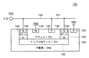
図4は、図1に示した入力バッファ12において、データ入出力端子DQj(j=0〜i)の各々に対応して設けられるクランプ回路100の構成を示す断面図である。
【0136】
クランプ回路100においては、基板電位発生回路30により供給される基板電位Vbbが、P型拡散領域122を介して供給されている。
【0137】
P型基板120の主表面側には、P型ウェル130が設けられ、このP型ウェル130の周囲を取囲むように、N型ウェル140が形成され、P型ウェル150底部の基板中には、トリプルN型ウェル150が設けられている。したがって、P型ウェル130は、N型ウェル140とトリプルN型ウェル150とによりその主表面側を除いて完全に取囲まれる構成となっている。
【0138】
図4に示したクランプ回路100においては、さらに、データ入出力端子DQjからの入力信号(電位レベル:Vin)を伝達する入力信号配線102とN型ウェル140とは、N型ウェル140の主表面側に形成されるN型拡散領域142を介して接続されている。
【0139】
また、入力信号配線102と、P型ウェル130とは、P型ウェルの主表面側に形成されるP型拡散領域132を介して、電気的に接続されている。
【0140】
さらに、P型ウェル130の主表面側には、N型拡散領域134が設けられ、このN型拡散領域134には、外部電源電位Vddが印加される構成となっている。
【0141】
図4に示したクランプ回路100においては、以上のような構成とすることで、入力信号がオーバーシュートして、その電位レベルが電位Vdd+Vbi(VbiはPN接合の立上がり電圧)よりも高くなると、外部電源電位Vddが供給されるN型拡散領域134とP型ウェル130とが順方向にバイアスされることになる。このため、N型拡散領域134から電子がP型ウェルに流入してくる。このようにしてP型ウェル130に注入された電子は、P型ウェル130、もしくはまわりのN型ウェル140またはトリプルN型ウェル150にすべて吸収され、オーバーシュートがクランプされる。
【0142】
また、P型基板120には全く電流が流入しないため、P型基板の電位は基板電位Vbbとすることが可能である。
【0143】
以上のようなクランプ回路100の構成とすることで、入力信号がオーバーシュートしようとする際に、その入力信号を伝達する入力信号配線102の電位レベルをクランプするクランプ回路100を、P型基板120の電位レベルを負電位である基板電位Vbbとしたままで実現することが可能である。
【0144】
したがって、クランプ回路100は、たとえば、図19に示したようなDRAMが形成されるP型基板上に同時に形成することが可能である。
【0145】
[実施の形態2]
図5は、本発明の実施の形態2のクランプ回路200の構成を示す断面図である。
【0146】
図5を参照して、P型基板120は、その主表面側に形成されるP型拡散領域222を介して、基板電位発生回路30から、基板電位Vbbの供給を受けている。
【0147】
P型基板120の主表面側には、P型ウェル230が形成されている。
P型ウェル230の周囲を取囲むように、N型ウェル240が形成され、P型ウェル230の底面と、P型基板220との境界領域には、トリプルN型ウェル250が形成されている。
【0148】
したがって、P型ウェル230は、N型ウェル240およびトリプルN型ウェル250とにより、その主表面側を除いて、完全に取囲まれる構成となっている。
【0149】
N型ウェル240は、その主表面側に形成されたN型拡散領域242を介して、接地電位GNDを受けている。
【0150】
P型ウェル230も、その主表面側に形成されたP型拡散領域232を介して、接地電位GNDを受けている。
【0151】
さらに、P型ウェル230の主表面側には、N型拡散領域234が形成されている。
【0152】
N型拡散領域234は、外部からの信号を受ける端子(たとえば、データ入出力端子DQj)からの入力信号を伝達する入力信号配線102と電気的に結合している。
【0153】
以上のような構成とすることにより、入力信号の電位レベルが−Vbi以下になると、N型拡散領域234とP型ウェル230とが順方向にバイアスされることになる。
【0154】
このため、電子が、N型拡散領域234からP型ウェル230に流入する。これらの電子は、P型ウェル230、N型ウェル240、トリプルN型ウェル250にすべて吸収され、入力信号は接地電位GNDにクランプされる。
【0155】
このような構成では、P型基板120には、クランプ動作中に電流が流れないので、P型基板の電位レベルは基板電位Vbbとすることが可能である。
【0156】
これに対して、もしもトリプルN型ウェル250が存在しない場合は、P型ウェル230の電位レベルは電位Vbbとなる。このため、入力信号のレベルが−|Vbb|−Vbi以下にならないと、N型拡散層234およびP型ウェル230から構成されるPN接合は順方向にならず、クランプ回路200のクランプ特性は劣化してしまう。
【0157】
したがって、図5に示したような構成とすることで、P型基板の電位レベルを基板電位Vbbに維持したまま、入力信号配線102の電位レベルの接地電位側へのクランプ特性も向上させることが可能となる。
【0158】
なお、以上の説明では、N型ウェル240およびトリプルN型ウェル250の電位レベルは接地電位GNDに保持されるものとした。
【0159】
しかしながら、本発明はこのような場合に限定されることなく、たとえば、P型ウェル230の電位レベルを接地電位GNDとし、N型ウェル240およびトリプルN型ウェル250の電位レベルを外部電源電位Vddとすることも可能である。
【0160】
[実施の形態3]
図6は、本発明の実施の形態3のクランプ回路300の構成を示す断面図である。
【0161】
クランプ回路300の構成は、実施の形態1で示した外部電源電位Vdd側に対するクランプ回路100と、接地電位GND側に対するクランプ回路200とを、ともに外部からの信号を受ける端子(たとえば、データ入出力端子DQj)からの信号を伝達する入出信号配線102に接続する構成としたものである。
【0162】
ただし、図6においては、P型ウェル130において、P型拡散領域132は、N型拡散領域134の両側に設けられている。
【0163】
また、P型ウェル230において、N型拡散領域234は、P型拡散領域232の両側に設けられている。
【0164】
その他、実施の形態1のクランプ回路100および実施の形態2のクランプ回路200と同一部分には同一符号を付して、その説明は繰返さない。
【0165】
図6に示したような構成とすることで、クランプ回路300は、入力信号の電位レベルが、外部電源電位Vddに対してオーバーシュートした場合でも、接地電位GNDに対してアンダーシュートした場合にも、入力信号配線102の電位レベルをクランプすることが可能である。
【0166】
しかも、この場合、基板120の電位レベルは、基板電位発生回路30から供給される基板電位Vbbに維持することが可能である。
【0167】
図7は、図6に示したクランプ回路の構成の平面パターンの一例を示す図である。
【0168】
図7中のBB’断面が、図6に示したクランプ回路300の断面構造に対応する。
【0169】
図7においては、P型ウェル130を取囲むように、N型ウェル140が形成されている。
【0170】
P型ウェル130には、その長辺方向に沿って、長方形形状を有するP型拡散領域132が2つ設けられている。
【0171】
さらに、この2つのP型拡散領域132に挟まれるように、P型ウェル130の長辺方向に沿って、N型拡散領域134が形成されている。
【0172】
N型ウェル140においても、P型ウェルを取囲むように、N型拡散領域142が形成されている。
【0173】
一方、P型ウェル230を取囲むように、N型ウェル240が形成されている。
【0174】
P型ウェル領域230中には、その長辺方向に沿って、長方形形状を有するN型拡散領域234が2本形成されている。
【0175】
N型拡散領域234に挟まれるように、P型ウェル230の長辺方向に沿って、P型拡散領域232が設けられている。
【0176】
また、N型ウェル240には、P型ウェル230を取囲むように、N型拡散領域242が設けられている。
【0177】
図7に示した構成においては、N型拡散領域134に対して、メタル配線402により外部電源電位Vddが供給されている。
【0178】
一方、N型ウェル240に対しては、拡散領域242を介して、メタル配線404から接地電位GNDが供給されている。
【0179】
P型ウェル230に対しては、P型拡散領域232を介して、メタル配線404から接地電位GNDが供給されている。
【0180】
また、入力信号配線102は、N型拡散領域142を介して、N型ウェル140と、P型拡散領域132を介して、P型ウェル130と接続されている。
【0181】
さらに、入力信号配線102は、N型拡散領域234と接続されている。
このような構成とすることで、図6に示した断面構造を有するクランプ回路300を実現することが可能となる。
【0182】
[実施の形態3の変形例1]
図8は、図6に示したクランプ回路と同様の機能を有する構成を実現する他の配線パターンを示す図である。
【0183】
図8においては、P型ウェル130を取囲むように、N型ウェル140が形成されている。
【0184】
P型ウェル130には、その長辺方向に沿って、長方形形状を有するN型拡散領域134が2つ設けられている。
【0185】
さらに、この2つのN型拡散領域134に挟まれるように、P型ウェル130の長辺方向に沿って、P型拡散領域132が形成されている。
【0186】
N型ウェル140においても、P型ウェルを取囲むように、N型拡散領域142が形成されている。
【0187】
入力信号配線102は、N型拡散領域142を介してN型ウェル140と、P型拡散領域132を介してP型ウェル130と、それぞれ接続されている。
【0188】
N型拡散領域134には、メタル配線402から電源電位Vddが供給される。
【0189】
一方、P型ウェル230およびN型ウェル240部分の構成は、図7に示した構成と同様であるので、同一部分には同一符号を付して説明は繰り返さない。
【0190】
このような構成とすることで、図6に示した断面構造を有するクランプ回路300と同様の機能を有するクランプ回路を実現することが可能となる。
【0191】
[実施の形態3の変形例2]
図9は、図6に示したクランプ回路と同様の機能を有するクランプ回路の平面パターンの他の例を示す平面図である。
【0192】
図9においては、P型ウェル230を取囲むように、N型ウェル240が形成されている。
【0193】
P型ウェル230には、その長辺方向に沿って、長方形形状を有するP型拡散領域232が2つ設けられている。
【0194】
さらに、この2つのP型拡散領域232に挟まれるように、P型ウェル230の長辺方向に沿って、N型拡散領域234が形成されている。
【0195】
N型ウェル240においても、P型ウェル230を取囲むように、N型拡散領域242が形成されている。
【0196】
N型拡散領域234は、入力信号配線102と接続している。
さらに、P型ウェル230はP型拡散領域232を介して、N型ウェル240はN型拡散領域242を介して、それぞれメタル配線404から接地電位GNDが供給される。
【0197】
一方、P型ウェル130およびN型ウェル140部分の構成は、図7に示した構成と同様であるので、同一部分には同一符号を付して説明は繰り返さない。
【0198】
このような構成とすることで、図6に示した断面構造を有するクランプ回路300と同様の機能を有するクランプ回路を実現することが可能となる。
【0199】
[実施の形態3の変形例3]
図10は、図6に示したクランプ回路300と同様の機能を有するクランプ回路の平面パターンの他の例を示す平面図である。
【0200】
図10においては、P型ウェル130を取囲むように、N型ウェル140が形成されている。
【0201】
P型ウェル130には、その長辺方向に沿って、長方形形状を有するN型拡散領域134が2つ設けられている。
【0202】
さらに、この2つのN型拡散領域134に挟まれるように、P型ウェル130の長辺方向に沿って、P型拡散領域132が形成されている。
【0203】
N型ウェル140においても、P型ウェルを取囲むように、N型拡散領域142が形成されている。
【0204】
入力信号配線102は、N型拡散領域142を介してN型ウェル140と、P型拡散領域132を介してP型ウェル130と、それぞれ接続されている。
【0205】
N型拡散領域134は、メタル配線402から電源電位Vddが供給される。
一方、P型ウェル230およびN型ウェル240部分の構成は、図9に示した構成と同様であるので、同一部分には同一符号を付して説明は繰り返さない。
【0206】
このような構成とすることで、図6に示した断面構造を有するクランプ回路300と同様の機能を有するクランプ回路を実現することが可能となる。
【0207】
図11は、図6に示したクランプ回路300を、図19に示したようなDRAM回路と同一基板上に形成した場合の構成を示す断面図である。
【0208】
図19に示したDRAMおよび図6に示したクランプ回路300の構成と同一部分には同一符号を付してその説明は繰返さない。
【0209】
以上のような構成とすることで、DRAMを形成している基板上に、PN接合を用いて、電源電位側に対するオーバーシュートおよび接地電位側に対するアンダーシュートのいずれをもクランプすることが可能なクランプ回路を搭載することが可能となる。
【0210】
したがって、入力サージ等に対する耐性が強く、クランプ能力の大きなクランプ回路をDRAMと同一基板上に形成することが可能となる。
【0211】
【発明の効果】
請求項1の半導体記憶装置は、第2の電源電位以上の入力信号が入力パッドに与えられた場合、第1の不純物ドーピング領域と、第2のウェル領域とで形成されるPN接合が順方向にバイアスされ、入力信号配線の電位レベルはクランプされる。PN接合を用いたクランプ回路であるため、電流吸収能力は高く、かつサージ入力に対しての耐性が高い。
【0212】
請求項2記載の半導体記憶装置は、請求項1記載の半導体記憶装置の構成に加えて、メモリセルアレイが形成される第3のウェル領域と、第2のウェル領域とが、第1のウェル領域により電気的に分離されているので、メモリセルアレイ部の基板電位を負電位に維持することが可能である。
【0213】
請求項3ないし5記載の半導体記憶装置は、第1の電源電位以下の入力信号が入力パッドに与えられた場合、第2の不純物ドーピング領域と、第2のウェル領域とで形成されるPN接合が順方向にバイアスされ、入力信号配線の電位レベルはクランプされる。PN接合を用いたクランプ回路であるため、電流吸収能力は高く、かつサージ入力に対しての耐性が高い。
【0214】
請求項6記載の半導体記憶装置は、請求項3記載の半導体記憶装置の構成に加えて、メモリセルアレイが形成される第3のウェル領域と、第2のウェル領域とが、第1のウェル領域により電気的に分離されているので、メモリセルアレイ部の基板電位を負電位に維持することが可能である。
【図面の簡単な説明】
【図1】 本発明の実施の形態1の半導体記憶装置1000の構成を示す概略ブロック図である。
【図2】 図1に示す1つのメモリセルプレーンの構成を具体的に示す図である。
【図3】 図2に示すセンスアンプ帯の配置を具体的に示す図である。
【図4】 本発明の実施の形態1のクランプ回路100の構成を示す断面図である。
【図5】 本発明の実施の形態2のクランプ回路200の構成を示す断面図である。
【図6】 本発明の実施の形態3のクランプ回路300の構成を示す断面図である。
【図7】 図6に示したクランプ回路300の構成を示す平面図である。
【図8】 実施の形態3の第1の変形例の平面パターンを示す図である。
【図9】 実施の形態3の第2の変形例の平面パターンを示す図である。
【図10】 実施の形態3の第3の変形例の平面パターンを示す図である。
【図11】 実施の形態3のクランプ回路とDRAMを同一基板上に形成した場合の断面構造を示す図である。
【図12】 入力信号の時間変化を示すタイミングチャートである。
【図13】 従来のクランプ回路700の構成を示す回路図である。
【図14】 図13に示したクランプ回路700の構成を示す断面図である。
【図15】 従来のクランプ回路800の構成を示す回路図である。
【図16】 図15に示したクランプ回路800の構成を示す断面図である。
【図17】 従来のクランプ回路900の構成を示す回路図である。
【図18】 図17に示したクランプ回路900の構成を示す断面図である。
【図19】 従来のDRAMの構成を示す断面図である。
【図20】 従来のDRAMのメモリセルの平面パターンを示す図である。
【図21】 従来のDRAMの他の構成を示す断面図である。
【図22】 従来のDRAMの他の例を示す断面図である。
【符号の説明】
3 アドレスバッファ、4 ATD発生回路、5 PAE発生回路、6 IOEQ発生回路、7,8 読出ドライバ、10 制御回路、11 ドライバ、12入力バッファ、13 出力バッファ、16 行選択回路、18 列選択回路、GIOa、GIOb、GIOc、GIOd グローバルIO線対、LIOa、LIOb、LIOc、LIOd ローカルIO線対、SABN、SABN+1 センスアンプ帯、MRBN 行ブロック、CSL 列選択線、100,200,300 クランプ回路、120,220,320 P型基板、130,230 P型ウェル、140,240 N型ウェル、150,250 トリプルN型ウェル、122,222 P型拡散層、132,232 P型拡散層、134,234N型拡散層、142,242 N型拡散層、1000 半導体記憶装置。[0001]
BACKGROUND OF THE INVENTION
The present invention relates to a semiconductor memory device, and more particularly to a configuration of a semiconductor memory device capable of operating in accordance with a signal applied from outside at high speed.
[0002]
[Prior art]
In order to operate the semiconductor memory device at high speed, it is necessary to sharply change the rise and fall of a signal input to the semiconductor memory device from the outside.
[0003]
For this reason, the driving power of the signal driver circuit of the external device that supplies data to the semiconductor memory device is set high.
[0004]
However, for example, an inductance component is parasitically equivalent as a distributed constant in the wiring on the board on which the semiconductor memory device is actually mounted. For this reason, the larger the time change rate of the input signal, the greater the disturbance of the signal waveform taken into the semiconductor memory device.
[0005]
FIG. 12 is a diagram showing the time change of the input signal waveform in the semiconductor memory device. In the figure, the “H” level of the input signal is assumed to be the level of the potential VIH, and the “L” level of the input signal is assumed to have the level of the potential VIL.
[0006]
It is assumed that the input signal starts to rise from “L” level toward “H” level at time t1. In this case, as described above, the signal waveform taken into the semiconductor memory device becomes a so-called overshoot waveform exceeding the potential level VIH.
[0007]
Similarly, at time t2, the input signal is assumed to fall from the “H” level to the “L” level. Also at this time, an undershoot exists in the input signal waveform due to the parasitic inductance component existing in the wiring on the board.
[0008]
However, if such an overshoot or undershoot exists in the input signal waveform, the operation of the semiconductor memory device becomes unstable, and the operation of the system itself configured on the board on which the semiconductor memory device is mounted is reduced. Stability is also impaired.
[0009]
Therefore, generally, on the semiconductor memory device side, the input signal waveform is shaped to suppress the occurrence of overshoot or undershoot of the input signal.
[0010]
FIG. 13 is a circuit diagram showing a configuration of a
[0011]
Referring to FIG. 13, an N channel MOS transistor Q1 is provided between
[0012]
Similarly, the gate of N channel MOS transistor Q2 is coupled to ground potential GND, and is diode-connected such that the direction from ground potential GND to
[0013]
FIG. 14 is a cross-sectional view for explaining a cross-sectional structure of the
[0014]
N channel MOS transistors Q1 and Q2 are both provided in P type well 722 formed on the main surface side of
[0015]
P-
[0016]
In the configuration of
[0017]
At this time, since the back bias of N channel MOS transistor Q1 is potential Vbb, when a clamping operation is performed, potential Vsb between the source substrates of N channel MOS transistor Q1 is Vsb = Vdd + | Vbb |. Therefore, the N channel MOS transistor receives a large substrate effect. Here, | Vbb | is the absolute value of the substrate potential Vbb.
[0018]
Therefore, if the threshold voltage Vth of the N-channel MOS transistor is 0.8 V in a normal substrate bias state, this threshold voltage rises to, for example, about Vth = 1.2 V due to a large substrate effect. To do.
[0019]
For this reason, the configuration of the
[0020]
Further, the configurations shown in FIG. 13 and FIG. 14 have a drawback that the tolerance against an input surge is poor. This is because both of the clamp elements are formed of N-channel MOS transistors, so that the oxide film destruction of the N-channel MOS transistors occurs due to an input surge. For this reason, the configuration of the
[0021]
FIG. 15 is a circuit diagram showing a configuration of a
[0022]
In
[0023]
The gate of P channel MOS transistor Q3 is coupled to power supply potential Vdd, and is therefore diode-connected so that the direction from
[0024]
The other points are similar to the configuration of
[0025]
16 is a cross-sectional view for explaining a cross-sectional structure of
[0026]
P-channel MOS transistor Q3 is provided in N-type well 820 formed on the main surface side of P-
[0027]
N-
[0028]
At this time, the P-
This is due to the reason explained below.
[0029]
That is, in the configuration of the
[0030]
In this way, the clamp current flows from the P-
[0031]
When such a clamp current flows into the substrate, the substrate becomes a positive potential. This induces a latch-up phenomenon of the CMOS circuit, which is fatal for normal operation of the DRAM.
[0032]
Therefore, the
[0033]
On the other hand, when operating as a clamp element, the PN junction has the advantage of having a larger current absorption capability than the MOS transistor.
[0034]
Therefore, it can be said that the configuration of the
[0035]
FIG. 17 is a circuit diagram showing a configuration of a
[0036]
In the
[0037]
FIG. 18 is a cross-sectional view for explaining a cross-sectional structure of the
[0038]
In FIG. 18, a power supply potential Vdd is supplied to an N well 820 formed on the main surface side of a P-
[0039]
On the other hand, a ground potential GND is supplied to a P well 922 provided adjacent to the N well 920.
[0040]
The
[0041]
With such a configuration, as in the
[0042]
Therefore, as in the case of FIG. 16, the clamp current flows from the P-
[0043]
In this case, since the clamp element is a PN junction diode, the current absorption capability is greater than when a MOS transistor is used. Further, when a PN junction diode is used, there is an advantage that the oxide film is not destroyed by the input surge because there is no oxide film in the clamp element.
[0044]
Therefore, the advantage of configuring the clamp circuit by using a PN junction diode is great.
[0045]
[Problems to be solved by the invention]
FIG. 19 is a diagram showing a cross-sectional structure of a memory cell array portion in a semiconductor memory device, particularly a dynamic random access memory (hereinafter referred to as DRAM), and FIG. 20 is a plan view showing a configuration of the memory cell array.
[0046]
Referring to FIG. 19, first, P-
[0047]
In general, each memory cell includes one N
[0048]
Here, N
[0049]
P-
[0050]
In P-
[0051]
An N-
[0052]
Further, another N-
[0053]
N-
[0054]
Referring to FIG. 20, the memory cell array is divided into a plurality of memory cell blocks, and sense amplifier bands SAB are arranged corresponding to the memory cell blocks. Further, corresponding to each memory cell block, a word driver band WDB provided with the word driver circuit shown in FIG. 19 is provided in a direction crossing the sense amplifier band.
[0055]
FIG. 21 is a cross-sectional view showing another example of a memory cell array configuration of a conventionally used DRAM.
[0056]
The planar configuration of the memory cell array shown in FIG. 21 is the same as that of the memory cell array shown in FIG.
[0057]
Also in the configuration shown in FIG. 21, the N-
[0058]
This P-
[0059]
Further, an N-
[0060]
Here, the configuration shown in FIG. 21 is different from the configuration shown in FIG. 19 in that a word driver circuit for driving a word line is configured only by an N-
[0061]
Therefore, in the configuration shown in FIG. 21, a so-called self-boost type circuit is used for the word driver.
[0062]
Therefore, in the configuration shown in FIG. 21, in order to drive the potential level of the word line, the word driver circuit needs an order sequence in which the boost operation is performed after the precharge operation.
[0063]
Therefore, there is a disadvantage that it takes more time to activate the word line than the configuration shown in FIG. 19 and the access speed is delayed.
[0064]
Here, in both FIG. 19 and FIG. 21, the potential level of the P-type substrate is maintained at the potential level of the P-type well, that is, the substrate potential Vbb.
[0065]
Therefore, if the
[0066]
That is, in both the
[0067]
On the other hand, in both the configuration shown in FIG. 19 and the configuration shown in FIG. 21, the potential level of the P-type substrate must be the substrate potential Vbb. Therefore, the
[0068]
In order to solve such problems, it is possible to use a DRAM structure having a cross-sectional structure as shown in FIG.
[0069]
That is, the cross-sectional structure of the DRAM shown in FIG. 22 differs from the cross-sectional structure of the DRAM shown in FIG. 19 in the following points.
[0070]
That is, in the DRAM configuration shown in FIG. 22, the P-
[0071]
That is, with the configuration shown in FIG. 22, the potential level of P-
[0072]
However, the configuration as shown in FIG. 22 has the following problems.
[0073]
That is, in the configuration shown in FIG. 22, the P-
[0074]
At this time, N-
[0075]
On the other hand, the N-type well 742 provided with the P-channel
[0076]
Providing such an isolation band causes an increase in the area of the memory cell array when a plurality of sense amplifier bands are provided in the memory cell array, as shown in FIG. Will increase.
[0077]
In order to set the potential level of the P-type well 740 to the substrate potential Vbb and the potential level of the P-type substrate to the ground potential GND, for example, there is a method of fixing the potential level of the triple N-type well 746 to Vcc.
[0078]
In this case, the P-
[0079]
In this case, an isolation band is required between the N-type well 744 where the P-
[0080]
Accordingly, in this case as well, as shown in FIG. 20, when a plurality of word drivers are provided in the memory cell array, the area of the memory cell array is increased, and consequently the chip area is increased.
[0081]
The present invention has been made to solve the above-described problems, and an object thereof is to provide a DRAM capable of mounting a clamp circuit using a PN junction.
[0082]
Still another object of the present invention is to provide a DRAM capable of suppressing an increase in chip area even when a clamp circuit using a PN junction is mounted.
[0083]
[Means for Solving the Problems]
2. The semiconductor memory device according to
[0084]
In addition to the configuration of the semiconductor memory device according to
[0085]
4. The semiconductor memory device according to
[0086]
According to a fourth aspect of the present invention, in the semiconductor memory device according to the third aspect, the predetermined potential is the first power supply potential.
[0087]
According to a fifth aspect of the present invention, in the semiconductor memory device according to the third aspect, the predetermined potential is the second power supply potential.
[0088]
In addition to the configuration of the semiconductor memory device according to
[0089]
DETAILED DESCRIPTION OF THE INVENTION
[Embodiment 1]
FIG. 1 is a schematic block diagram showing the configuration of the
[0090]
Referring to FIG. 1,
[0091]
Each of memory cell planes M # 0 to
[0092]
The
[0093]
As will be described later, in FIG. 1, the word line driver or the like is assumed to exist only on one side of the long side of the memory cell plane, but in reality, a plurality of strips are formed in the memory cell plane. Is arranged.
[0094]
Each of memory cell planes M # 0-
[0095]
[0096]
Preamplifier / write buffer 7 transmits memory cell data of a selected column group onto corresponding read data buses RDABa to RDABd via read driver 8 in each of memory cell planes M # 0 to
[0097]
A write buffer of preamplifier / write buffer 7 is coupled to input
[0098]
[0099]
Here, the global IO line pair GIOP is composed of complementary signal line pairs, and transmits mutually complementary data signals. The potentials of the global IO lines of the global IO line pair GIOP are made equal by the equalize signal IOEQ.
[0100]
[0101]
Internal power supply potential Vcc is applied to a circuit for driving memory cell planes M # 0 to M # 3 (a sense amplifier for charging / discharging bit lines) and a well in which p channel MOS transistors in the array are formed.
[0102]
The
[0103]
Further, a
[0104]
Specifically, the
[0105]
However, for the sake of simplicity, the following description will be made by taking the
[0106]
FIG. 2 is a diagram showing in more detail the configuration of a portion related to one memory cell plane M # (hereinafter referred to as M # when generically referred to as M # 0 to M # 3).
[0107]
In FIG. 2, memory cell plane M # is divided into 16 row blocks MRB0-MRB15 along the column direction. Memory cell plane M # is further divided into 16 column blocks MCB0 to MCB15 along the row direction.
[0108]
That is, memory cell plane M # includes memory cell block MCnn for each region where row block MRBn (n = 0-15) and column block MCBn (n = 0-15) intersect. In each memory cell block MCnn, 64K-bit memory cells are arranged in a matrix of rows and columns.
[0109]
Sense amplifier bands SAB1 to SAB15 having sense amplifiers for detecting and amplifying data of memory cells selected according to the external address signal are arranged in regions between row blocks MRB0 to MRB15.
[0110]
Sense amplifier bands SAB0 and SAB16 are further arranged outside row blocks MRB0 to MRB15, respectively.
[0111]
One row block MRBn (n = 0 to 15) includes data of memory cells connected to one selected row by sense amplifiers included in sense amplifier bands SABn and SAB (n + 1) arranged on both sides thereof. Detection and amplification are performed.
[0112]
Therefore, sense amplifier bands SAB1 to SAB15 are configured to be shared by two row blocks.
[0113]
In the region between column blocks MCB0-MCB15, word driver bands WD1-WD15 having word drivers for activating word lines selected according to the external address signal are arranged.
[0114]
Word driver bands WD0 and WD16 are further arranged outside column blocks MCB0 to MCB15, respectively.
[0115]
In one column block MCBn (n = 0-15), the word driver corresponding to the selected row is activated by the word drivers included in word driver bands WDn and WD (n + 1) arranged on both sides thereof. It is.
[0116]
Therefore, the word driver bands WD1 to WD15 are shared by the two column blocks.
[0117]
FIG. 3 is a circuit diagram more specifically showing the configuration of sense amplifier bands SABN and SABN + 1 shown in FIG.
[0118]
FIG. 3 representatively shows a configuration of a portion related to one column selection line CSL.
[0119]
Only the column selection line CSL in the column block selected according to the address signal from the outside is selected, that is, its potential level is set to the “H” level.
[0120]
For example, four bit line pairs BLP0 to BLP3 are arranged for one column selection line CSL. Bit line pairs BLP0 to BLP3 each include bit lines BL and / BL transmitting mutually complementary signals. Corresponding memory cells MC are arranged at intersections between the bit line pairs BLP0 to BLP3 and the word line WL.
[0121]
FIG. 3 shows, as an example, a state in which memory cells MC are arranged corresponding to intersections between bit lines BL and specific word lines WL.
[0122]
Memory cell MC includes an access transistor rendered conductive by word line WL, and a memory cell capacitor to which a corresponding bit line and one electrode are connected by the access transistor.
[0123]
The other electrode of the memory cell capacitor is supplied with a cell plate potential Vcp (generally, a potential that is half the potential Vcc).
[0124]
Bit line pair BLP0 and BLP2 are connected to sense amplifiers SA0 and SA2 included in sense amplifier band SABN through isolation gates TGa0 and TGa2 which are turned on in response to bit line isolation control signal BRIb, respectively.
[0125]
Bit line pair BLP1 and BLP3 are connected to sense amplifiers SA1 and SA3 included in sense amplifier band SABN + 1 through isolation gates TGa1 and TGa3 which are turned on in response to bit line isolation control signal BLIa, respectively.
[0126]
Sense amplifier SA included in sense amplifier band SABN is connected to a bit line pair included in row block MRB (N−1) via isolation gates TGb0 and TGb2 that are turned on in response to isolation control signal BLIb. .
[0127]
Sense amplifier SA included in sense amplifier band SABN + 1 is connected to a bit line pair included in row block MRBN + 1 through isolation gates TGb1 and TGb3 which are turned on in response to isolation control signal BRRI.
[0128]
Sense amplifier SA is provided corresponding to each bit line pair and is shared by bit line pairs in adjacent row blocks. In one row block MRBN, the sense amplifiers SA are alternately arranged on both sides of the bit line pair and have a so-called alternately arranged shared sense amplifier arrangement.
[0129]
In sense amplifier band SABN, local IO line pairs LIOa and LIOb are arranged in parallel to word line WL and exist over one column block.
[0130]
In sense amplifier band SABN + 1, local IO line pairs LIOc and LIOd are similarly arranged.
[0131]
For each of sense amplifiers SA0-SA3, column selection gates IG0-IG3 that are turned on in response to a signal potential on column selection line CSL are provided. These column selection gates IG0 to IG3 are rendered conductive when the signal potential on the corresponding column selection line CSL is at "H" level indicating the selected state, and the sense amplifiers SA0 to SA3 are connected to the local IO line pairs LIOa to LIOd, respectively. Connect to.
When row block MRBN is selected, bit line isolation control signals BLIa and BRIb are set to “H” level, and bit line isolation control signals BRIa and BLIb are set to “L” level. Thereby, the bit line pairs BLP0 to BLP3 are connected to the sense amplifiers SA0 to SA3, respectively.
[0132]
In the standby state, bit line isolation control signals BLIa, BLIb, BRIa and BRIb are all set to the “H” level, and isolation control gates TGa0 to TGa3 and TGb0 to TGb3 are all turned on.
[0133]
On the other hand, in the read operation or the like, only the selected row block is connected to the sense amplifier SA, thereby reducing the capacity of the bit line pair connected to the sense amplifier SA, and sufficient for high-speed sense operation and sense node. Thus, it is possible to transmit a read voltage (read data of a memory cell).
[0134]
Local IO line pairs LIOa to LIOd are connected to global IO line pairs GIOa to GIOd arranged in corresponding column groups (not shown).
[0135]
FIG. 4 is a cross-sectional view showing a configuration of
[0136]
In the
[0137]
A P-
[0138]
In the
[0139]
Further, the
[0140]
Further, an N-
[0141]
In the
[0142]
Further, since no current flows into the P-
[0143]
With the configuration of the
[0144]
Therefore, for example, the
[0145]
[Embodiment 2]
FIG. 5 is a cross-sectional view showing the configuration of the
[0146]
Referring to FIG. 5,
[0147]
A P-
An N-
[0148]
Therefore, the P-
[0149]
N-
[0150]
P-type well 230 also receives ground potential GND via P-
[0151]
Further, an N-
[0152]
N-
[0153]
With the above configuration, when the potential level of the input signal becomes −Vbi or less, the N-
[0154]
For this reason, electrons flow from the N-
[0155]
In such a configuration, since no current flows through the P-
[0156]
On the other hand, if the triple N-
[0157]
Therefore, with the configuration as shown in FIG. 5, it is possible to improve the clamping characteristic of the potential level of the
[0158]
In the above description, the potential levels of the N-
[0159]
However, the present invention is not limited to such a case. For example, the potential level of P-
[0160]
[Embodiment 3]
FIG. 6 is a cross-sectional view showing the configuration of the
[0161]
The configuration of the
[0162]
However, in FIG. 6, in the P-
[0163]
In the P-
[0164]
In addition, the same reference numerals are given to the same portions as those of
[0165]
With the configuration as shown in FIG. 6, the
[0166]
In this case, the potential level of the
[0167]
FIG. 7 is a diagram showing an example of a planar pattern of the configuration of the clamp circuit shown in FIG.
[0168]
The BB ′ cross section in FIG. 7 corresponds to the cross sectional structure of the
[0169]
In FIG. 7, an N-
[0170]
The P-
[0171]
Further, an N-
[0172]
Also in the N-
[0173]
On the other hand, an N-
[0174]
In the P-
[0175]
A P-
[0176]
The N-
[0177]
In the configuration shown in FIG. 7, external power supply potential Vdd is supplied to N
[0178]
On the other hand, the ground potential GND is supplied from the
[0179]
A ground potential GND is supplied from the
[0180]
The
[0181]
Further, the
With such a configuration, the
[0182]
[
FIG. 8 is a diagram showing another wiring pattern that realizes a configuration having the same function as the clamp circuit shown in FIG.
[0183]
In FIG. 8, an N-
[0184]
Two N-
[0185]
Further, a P-
[0186]
Also in the N-
[0187]
The
[0188]
The power supply potential Vdd is supplied from the
[0189]
On the other hand, the configuration of the P-
[0190]
With such a configuration, a clamp circuit having the same function as the
[0191]
[
FIG. 9 is a plan view showing another example of a plane pattern of a clamp circuit having the same function as the clamp circuit shown in FIG.
[0192]
In FIG. 9, an N-
[0193]
The P-
[0194]
Further, an N-
[0195]
Also in the N-
[0196]
The N-
Further, the ground potential GND is supplied from the
[0197]
On the other hand, the configuration of the P-
[0198]
With such a configuration, a clamp circuit having the same function as the
[0199]
[
FIG. 10 is a plan view showing another example of a plane pattern of a clamp circuit having the same function as that of the
[0200]
In FIG. 10, an N-
[0201]
Two N-
[0202]
Further, a P-
[0203]
Also in the N-
[0204]
The
[0205]
N-
On the other hand, the structure of the P-
[0206]
With such a configuration, a clamp circuit having the same function as the
[0207]
FIG. 11 is a cross-sectional view showing a configuration when the
[0208]
The same parts as those of the DRAM shown in FIG. 19 and the
[0209]
With the above configuration, a clamp that can clamp both overshoots on the power supply potential side and undershoots on the ground potential side using a PN junction on the substrate on which the DRAM is formed. A circuit can be mounted.
[0210]
Therefore, it is possible to form a clamp circuit having a high resistance against an input surge or the like and having a large clamping capability on the same substrate as the DRAM.
[0211]
【The invention's effect】
According to another aspect of the semiconductor memory device of the present invention, when an input signal having a second power supply potential or higher is applied to the input pad, the PN junction formed by the first impurity doping region and the second well region is forward. And the potential level of the input signal wiring is clamped. Since it is a clamp circuit using a PN junction, the current absorption capability is high and the resistance against surge input is high.
[0212]
According to a second aspect of the present invention, in addition to the configuration of the first semiconductor memory device, the third well region in which the memory cell array is formed and the second well region include the first well region. Therefore, the substrate potential of the memory cell array portion can be maintained at a negative potential.
[0213]
6. The semiconductor memory device according to
[0214]
According to a sixth aspect of the present invention, in addition to the configuration of the third aspect, the third well region in which the memory cell array is formed and the second well region include the first well region. Therefore, the substrate potential of the memory cell array portion can be maintained at a negative potential.
[Brief description of the drawings]
FIG. 1 is a schematic block diagram showing a configuration of a
2 is a diagram specifically showing a configuration of one memory cell plane shown in FIG. 1; FIG.
3 is a diagram specifically showing an arrangement of sense amplifier bands shown in FIG. 2. FIG.
FIG. 4 is a cross-sectional view showing a configuration of a
FIG. 5 is a cross-sectional view showing a configuration of a
FIG. 6 is a sectional view showing a configuration of a
7 is a plan view showing a configuration of the
FIG. 8 is a diagram showing a planar pattern of a first modification of the third embodiment.
FIG. 9 is a diagram showing a planar pattern of a second modified example of the third embodiment.
FIG. 10 is a diagram showing a planar pattern of a third modification of the third embodiment.
FIG. 11 is a diagram showing a cross-sectional structure when the clamp circuit and the DRAM of the third embodiment are formed on the same substrate.
FIG. 12 is a timing chart showing a time change of an input signal.
13 is a circuit diagram showing a configuration of a
14 is a cross-sectional view showing a configuration of a
15 is a circuit diagram showing a configuration of a
16 is a cross-sectional view showing a configuration of a
17 is a circuit diagram showing a configuration of a
18 is a cross-sectional view showing a configuration of the
FIG. 19 is a cross-sectional view showing a configuration of a conventional DRAM.
FIG. 20 is a diagram showing a plane pattern of a memory cell of a conventional DRAM.
FIG. 21 is a cross-sectional view showing another configuration of a conventional DRAM.
FIG. 22 is a cross-sectional view showing another example of a conventional DRAM.
[Explanation of symbols]
3 address buffer, 4 ATD generation circuit, 5 PAE generation circuit, 6 IOEQ generation circuit, 7, 8 read driver, 10 control circuit, 11 driver, 12 input buffer, 13 output buffer, 16 row selection circuit, 18 column selection circuit, GIOa, GIOb, GIOc, GIOd Global IO line pair, LIOa, LIOb, LIOc, LIOd Local IO line pair, SABN, SABN + 1 sense amplifier band, MRBN row block, CSL column selection line, 100, 200, 300 Clamp circuit, 120, 220,320 P-type substrate, 130,230 P-type well, 140,240 N-type well, 150,250 Triple N-type well, 122,222 P-type diffusion layer, 132,232 P-type diffusion layer, 134,234 N-type diffusion Layer, 142,242 N-type diffusion layer, 1000 semiconductor Storage device.
Claims (2)
前記外部からの信号を受ける入力パッドと、
第1の電源電位を受ける第1の電源パッドと、
前記第1の電源電位よりも高い第2の電源電位を受ける第2の電源パッドと、
前記入力パッドに与えられた信号を伝達する入力信号配線と、
前記半導体基板の主表面に形成され、前記入力信号配線の電位レベルを受けるN型の第2のウェル領域と、
前記第2のウェル領域内に、前記第2のウェル領域に前記主表面以外を取囲まれるように形成され、前記入力信号配線の電位レベルを受けるP型の第3のウェル領域と、
前記第3のウェル領域の主表面側に形成され、前記第2の電源電位を受けるN型の第1の不純物ドーピング領域とを備える、半導体記憶装置。 A DRAM memory cell that holds data corresponding to an external signal is formed in a P-type first well region provided on the main surface side of a P-type semiconductor substrate to which a negative substrate potential is supplied. A semiconductor memory device,
An input pad for receiving the external signal;
A first power supply pad receiving a first power supply potential;
A second power supply pad receiving a second power supply potential higher than the first power supply potential;
An input signal wiring for transmitting a signal given to the input pad;
An N-type second well region formed on the main surface of the semiconductor substrate and receiving a potential level of the input signal wiring;
In the second well region, and wherein the formed so as to be surrounded except major surface to the second well region, a third well region of the P type which receives the potential level of the input signal lines,
A semiconductor memory device comprising: an N-type first impurity doping region formed on a main surface side of the third well region and receiving the second power supply potential.
外部からの信号を受ける入力パッドと、
第1の電源電位を受ける第1の電源パッドと、
前記第1の電源電位よりも高い第2の電源電位を受ける第2の電源パッドと、
前記第1の電源電位および前記第2の電源電位を受けて、負電位の基板電位を生成し、前記半導体基板に供給する基板電位生成手段と、
前記第1および第2の電源電位を受けて、前記第1および第2の電源電位の中間の値を有する内部電源電位を発生する降圧手段と、
前記入力パッドに与えられた信号を伝達する入力信号配線と、
前記半導体基板の主表面に形成され、前記入力信号配線の電位レベルを受けるN型の第1のウェル領域と、
前記第1のウェル領域内に、前記第1のウェル領域に前記主表面以外を取囲まれるように形成され、前記入力信号配線の電位レベルを受けるP型の第2のウェル領域と、
前記第2のウェル領域の主表面側に形成され、前記第2の電源電位を受けるN型の第1の不純物ドーピング領域と、
前記入力信号配線に与えられた信号に応じて、書込まれたデータを保持する内部回路とを備え、
前記内部回路は、
前記半導体基板の主表面に形成されるP型の第3のウェル領域と、
前記半導体基板の主表面に前記第3のウェル領域に隣接して形成され、前記内部電源電位が供給されるN型の第4のウェル領域と、
前記第3のウェル領域に形成されるメモリセルアレイとを含み、
前記メモリセルアレイは、
前記メモリセルアレイの行方向に配置される複数のワード線と、
前記メモリセルアレイの列方向に配置される複数のビット線対と、
前記ワード線と前記ビット線対との交点に配置されるメモリセルと、
読出動作において、前記ビット線対の電位差を選択されたメモリセルに保持されるデータに応じて、増幅するN型チャネルセンスアンプとを有し、
前記第4のウェル領域に形成され、読出動作において、前記ビット線対の電位差を選択されたメモリセルに保持されるデータに応じて、増幅するP型チャネルセンスアンプとを含む、半導体記憶装置。 A semiconductor memory device formed on a P-type semiconductor substrate,
An input pad for receiving an external signal;
A first power supply pad receiving a first power supply potential;
A second power supply pad receiving a second power supply potential higher than the first power supply potential;
Substrate potential generation means for receiving the first power supply potential and the second power supply potential, generating a negative substrate potential, and supplying the negative substrate potential to the semiconductor substrate;
Step-down means for receiving the first and second power supply potentials and generating an internal power supply potential having an intermediate value between the first and second power supply potentials;
An input signal wiring for transmitting a signal given to the input pad;
An N-type first well region formed on a main surface of the semiconductor substrate and receiving a potential level of the input signal wiring;
A P-type second well region that is formed in the first well region so as to be surrounded by the first well region except for the main surface, and receives a potential level of the input signal wiring;
An N-type first impurity doping region formed on the main surface side of the second well region and receiving the second power supply potential;
Depending on the signal applied to the input signal lines, and an internal circuit for holding the written data,
The internal circuit is
A P-type third well region formed on the main surface of the semiconductor substrate;
An N-type fourth well region formed on the main surface of the semiconductor substrate adjacent to the third well region and supplied with the internal power supply potential;
A memory cell array formed in the third well region,
The memory cell array includes:
A plurality of word lines arranged in a row direction of the memory cell array;
A plurality of bit line pairs arranged in the column direction of the memory cell array;
A memory cell disposed at an intersection of the word line and the bit line pair;
An N-type channel sense amplifier that amplifies the potential difference of the bit line pair in accordance with data held in a selected memory cell in a read operation;
Wherein formed in the fourth well region, in the reading operation, in accordance with the data held in the bit line pair of the memory cell selected potential difference, and a P-type channel sense amplifier for amplifying, semiconductors memory device .
Priority Applications (5)
| Application Number | Priority Date | Filing Date | Title |
|---|---|---|---|
| JP26605797A JP4330183B2 (en) | 1997-09-30 | 1997-09-30 | Semiconductor memory device |
| US09/045,567 US5905679A (en) | 1997-09-30 | 1998-03-23 | Semiconductor memory device clamping the overshoot and undershoot of input signal by circuit with PN junction |
| DE19819039A DE19819039B4 (en) | 1997-09-30 | 1998-04-28 | Semiconductor memory device |
| TW087106489A TW392160B (en) | 1997-09-30 | 1998-04-28 | Semiconductor memory device |
| KR1019980020815A KR100283542B1 (en) | 1997-09-30 | 1998-06-05 | Semiconductor memory device clamping the overshoot and undershoot of input signal by circuit with pn junction |
Applications Claiming Priority (1)
| Application Number | Priority Date | Filing Date | Title |
|---|---|---|---|
| JP26605797A JP4330183B2 (en) | 1997-09-30 | 1997-09-30 | Semiconductor memory device |
Publications (2)
| Publication Number | Publication Date |
|---|---|
| JPH11111943A JPH11111943A (en) | 1999-04-23 |
| JP4330183B2 true JP4330183B2 (en) | 2009-09-16 |
Family
ID=17425790
Family Applications (1)
| Application Number | Title | Priority Date | Filing Date |
|---|---|---|---|
| JP26605797A Expired - Fee Related JP4330183B2 (en) | 1997-09-30 | 1997-09-30 | Semiconductor memory device |
Country Status (5)
| Country | Link |
|---|---|
| US (1) | US5905679A (en) |
| JP (1) | JP4330183B2 (en) |
| KR (1) | KR100283542B1 (en) |
| DE (1) | DE19819039B4 (en) |
| TW (1) | TW392160B (en) |
Families Citing this family (14)
| Publication number | Priority date | Publication date | Assignee | Title |
|---|---|---|---|---|
| US6144221A (en) * | 1998-07-02 | 2000-11-07 | Seiko Epson Corporation | Voltage tolerant interface circuit |
| JP3506633B2 (en) * | 1999-04-09 | 2004-03-15 | 沖電気工業株式会社 | Semiconductor device |
| JP2002124580A (en) * | 2000-10-18 | 2002-04-26 | Yamaha Corp | Input protective circuit |
| US6909659B2 (en) * | 2001-08-30 | 2005-06-21 | Micron Technology, Inc. | Zero power chip standby mode |
| US6930930B2 (en) * | 2002-11-06 | 2005-08-16 | Infineon Technologies Ag | Using isolated p-well transistor arrangements to avoid leakage caused by word line/bit line shorts |
| US6891207B2 (en) * | 2003-01-09 | 2005-05-10 | International Business Machines Corporation | Electrostatic discharge protection networks for triple well semiconductor devices |
| JP5315604B2 (en) * | 2006-09-29 | 2013-10-16 | 富士通セミコンダクター株式会社 | Semiconductor integrated circuit |
| US8139697B2 (en) * | 2008-01-29 | 2012-03-20 | United Microelectronics Corp. | Sampling method and data recovery circuit using the same |
| CN102893398B (en) * | 2010-05-18 | 2016-01-20 | 飞思卡尔半导体公司 | Integrated circuit, electronic device and esd protection thereof |
| US8729951B1 (en) | 2012-11-27 | 2014-05-20 | Freescale Semiconductor, Inc. | Voltage ramp-up protection |
| DK3095944T3 (en) * | 2015-05-18 | 2021-03-01 | Iso Chemie Gmbh | Building section with a window frame |
| US10395035B2 (en) * | 2016-09-27 | 2019-08-27 | Intel Corporation | Photon emission attack resistance driver circuits |
| US9793258B1 (en) * | 2016-11-04 | 2017-10-17 | United Microelectronics Corp. | Electrostatic discharge device |
| JP2021027060A (en) * | 2019-07-31 | 2021-02-22 | セイコーエプソン株式会社 | Circuit device, light source device and electronic apparatus |
Family Cites Families (7)
| Publication number | Priority date | Publication date | Assignee | Title |
|---|---|---|---|---|
| US5181091A (en) * | 1988-04-29 | 1993-01-19 | Dallas Semiconductor Corp. | Integrated circuit with improved protection against negative transients |
| JP2633746B2 (en) * | 1991-05-27 | 1997-07-23 | 株式会社東芝 | Semiconductor device |
| JPH05121670A (en) * | 1991-10-25 | 1993-05-18 | Nec Corp | Semiconductor input protective device |
| JP2830630B2 (en) * | 1992-07-23 | 1998-12-02 | 日本電気株式会社 | Semiconductor device and manufacturing method thereof |
| JP3246807B2 (en) * | 1993-07-07 | 2002-01-15 | 株式会社東芝 | Semiconductor integrated circuit device |
| JPH0951078A (en) * | 1995-05-29 | 1997-02-18 | Mitsubishi Electric Corp | Semiconductor memory and semiconductor device |
| JPH0955483A (en) * | 1995-06-09 | 1997-02-25 | Mitsubishi Electric Corp | Semiconductor memory device |
-
1997
- 1997-09-30 JP JP26605797A patent/JP4330183B2/en not_active Expired - Fee Related
-
1998
- 1998-03-23 US US09/045,567 patent/US5905679A/en not_active Expired - Lifetime
- 1998-04-28 TW TW087106489A patent/TW392160B/en not_active IP Right Cessation
- 1998-04-28 DE DE19819039A patent/DE19819039B4/en not_active Expired - Fee Related
- 1998-06-05 KR KR1019980020815A patent/KR100283542B1/en not_active IP Right Cessation
Also Published As
| Publication number | Publication date |
|---|---|
| KR19990029217A (en) | 1999-04-26 |
| JPH11111943A (en) | 1999-04-23 |
| KR100283542B1 (en) | 2001-03-02 |
| TW392160B (en) | 2000-06-01 |
| DE19819039B4 (en) | 2004-02-12 |
| US5905679A (en) | 1999-05-18 |
| DE19819039A1 (en) | 1999-04-08 |
Similar Documents
| Publication | Publication Date | Title |
|---|---|---|
| JP3853513B2 (en) | Dynamic RAM | |
| JP4110115B2 (en) | Semiconductor memory device | |
| US6031779A (en) | Dynamic memory | |
| JP4037470B2 (en) | Semiconductor device | |
| US7230867B2 (en) | Semiconductor device | |
| US7995405B2 (en) | Semiconductor memory device having a sense amplifier circuit with decreased offset | |
| KR100452322B1 (en) | method for supplying power supply voltage in semiconductor memory device and circuit for supplying cell array power supply voltage | |
| JP4330183B2 (en) | Semiconductor memory device | |
| US4791616A (en) | Semiconductor memory device | |
| JP3970396B2 (en) | Semiconductor memory device | |
| US5966340A (en) | Semiconductor memory device having hierarchical word line structure | |
| JP4079522B2 (en) | Semiconductor integrated circuit device | |
| JPH11330410A (en) | Semiconductor memory device | |
| US7085187B2 (en) | Semiconductor storage device | |
| WO2017145312A1 (en) | Semiconductor storage device | |
| JP4767390B2 (en) | DRAM | |
| US6973002B2 (en) | Semiconductor integrated circuit comprising sense amplifier activating circuit for activating sense amplifier circuit | |
| US6674112B1 (en) | Semiconductor integrated circuit device | |
| JP3856249B2 (en) | Semiconductor integrated circuit device | |
| US7403408B2 (en) | Semiconductor memory device and semiconductor device | |
| JPH06326272A (en) | Semiconductor memory | |
| US6744658B2 (en) | Semiconductor memory device capable of holding write data for long time | |
| KR100395876B1 (en) | Ground voltage supply line structure of a dram device | |
| TW202038231A (en) | Semiconductor device | |
| JPH09199682A (en) | Dynamic memory and its driving method |
Legal Events
| Date | Code | Title | Description |
|---|---|---|---|
| A621 | Written request for application examination |
Free format text: JAPANESE INTERMEDIATE CODE: A621 Effective date: 20040922 |
|
| A977 | Report on retrieval |
Free format text: JAPANESE INTERMEDIATE CODE: A971007 Effective date: 20061227 |
|
| A131 | Notification of reasons for refusal |
Free format text: JAPANESE INTERMEDIATE CODE: A131 Effective date: 20071120 |
|
| A521 | Request for written amendment filed |
Free format text: JAPANESE INTERMEDIATE CODE: A523 Effective date: 20080118 |
|
| TRDD | Decision of grant or rejection written | ||
| A01 | Written decision to grant a patent or to grant a registration (utility model) |
Free format text: JAPANESE INTERMEDIATE CODE: A01 Effective date: 20090609 |
|
| A01 | Written decision to grant a patent or to grant a registration (utility model) |
Free format text: JAPANESE INTERMEDIATE CODE: A01 |
|
| A61 | First payment of annual fees (during grant procedure) |
Free format text: JAPANESE INTERMEDIATE CODE: A61 Effective date: 20090616 |
|
| R150 | Certificate of patent or registration of utility model |
Free format text: JAPANESE INTERMEDIATE CODE: R150 |
|
| FPAY | Renewal fee payment (event date is renewal date of database) |
Free format text: PAYMENT UNTIL: 20120626 Year of fee payment: 3 |
|
| FPAY | Renewal fee payment (event date is renewal date of database) |
Free format text: PAYMENT UNTIL: 20120626 Year of fee payment: 3 |
|
| S111 | Request for change of ownership or part of ownership |
Free format text: JAPANESE INTERMEDIATE CODE: R313111 |
|
| FPAY | Renewal fee payment (event date is renewal date of database) |
Free format text: PAYMENT UNTIL: 20120626 Year of fee payment: 3 |
|
| R350 | Written notification of registration of transfer |
Free format text: JAPANESE INTERMEDIATE CODE: R350 |
|
| FPAY | Renewal fee payment (event date is renewal date of database) |
Free format text: PAYMENT UNTIL: 20120626 Year of fee payment: 3 |
|
| FPAY | Renewal fee payment (event date is renewal date of database) |
Free format text: PAYMENT UNTIL: 20130626 Year of fee payment: 4 |
|
| FPAY | Renewal fee payment (event date is renewal date of database) |
Free format text: PAYMENT UNTIL: 20130626 Year of fee payment: 4 |
|
| FPAY | Renewal fee payment (event date is renewal date of database) |
Free format text: PAYMENT UNTIL: 20140626 Year of fee payment: 5 |
|
| LAPS | Cancellation because of no payment of annual fees |