EP0535403B1 - Empfang eines digitalen TDMA-Datensignals mit Kompensation von Kanaländerungen - Google Patents
Empfang eines digitalen TDMA-Datensignals mit Kompensation von Kanaländerungen Download PDFInfo
- Publication number
- EP0535403B1 EP0535403B1 EP92115284A EP92115284A EP0535403B1 EP 0535403 B1 EP0535403 B1 EP 0535403B1 EP 92115284 A EP92115284 A EP 92115284A EP 92115284 A EP92115284 A EP 92115284A EP 0535403 B1 EP0535403 B1 EP 0535403B1
- Authority
- EP
- European Patent Office
- Prior art keywords
- channel impulse
- impulse response
- symbols
- time slot
- digital data
- Prior art date
- Legal status (The legal status is an assumption and is not a legal conclusion. Google has not performed a legal analysis and makes no representation as to the accuracy of the status listed.)
- Expired - Lifetime
Links
Images




Classifications
-
- H—ELECTRICITY
- H04—ELECTRIC COMMUNICATION TECHNIQUE
- H04L—TRANSMISSION OF DIGITAL INFORMATION, e.g. TELEGRAPHIC COMMUNICATION
- H04L25/00—Baseband systems
- H04L25/02—Details ; arrangements for supplying electrical power along data transmission lines
- H04L25/0202—Channel estimation
- H04L25/0224—Channel estimation using sounding signals
- H04L25/0228—Channel estimation using sounding signals with direct estimation from sounding signals
- H04L25/023—Channel estimation using sounding signals with direct estimation from sounding signals with extension to other symbols
- H04L25/0232—Channel estimation using sounding signals with direct estimation from sounding signals with extension to other symbols by interpolation between sounding signals
Definitions
- the present invention relates to a method of and an apparatus for successively receiving digital data signals using the time-division multiplex access (TDMA) technique and automatically equalizing and demodulating the received digital data signals into output signals based on channel impulse response extracted from the received digital data signals.
- TDMA time-division multiplex access
- data transmission in a TDMA system involves the successive transmission of N-channel data signals in a frame format 32 that are allocated respectively to N time slots 30, 31, each composed of N symbols.
- the first symbol Np of the frame in each of the time slots 30, 31 comprises a training sequence.
- data receivers in such a TDMA system extract channel impulse response using the training sequences in the received time slots for initializing equalizers and demodulate the received data signal in each of the time slots.
- the system includes an input terminal 70, an output terminal 71, a channel estimator 72, and a demodulator 73.
- the channel estimator 72 estimates channel impulse response using a received signal from the input terminal 70 and a decision result from the demodulator 73 to compensate for channel variations (see, for example, K. Okanoue, Improvements on Tracking Performances of Adaptive Viterbi MLSE Receiver, trans. of 1991 Spring National Conference, Institute of Electronics, Information and Communication Engineers, Tokyo, SB-4-4, pp. 2 - 624, 625, Mar. 1991).
- FIG. 3 of the accompanying drawings Another proposed system, which is shown in FIG. 3 of the accompanying drawings, has an input terminal 80, an output terminal 81, a channel estimator 82, and a demodulator 83.
- the channel estimator 82 establishes an equalizer using only received signals from the input terminal 80 and not a priori channel impulse response to compensate for channel variations (see, for example, A. Ushirokawa et al., Viterbi Equalization on Time-varying Channel, 2nd Makuhari Int. Conf. on High Tech., Chiba, A-2-2, pp. 101 - 104, Jan. 1991).
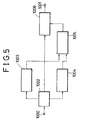
- FIGs. 4 and 5 of the accompanying drawings show still another proposed system.
- the system employs a signal format including at least two training sequences 91, 92 in one time slot 90 and interpolates a plurality of results estimated from the training sequence signals into channel information.
- An equalizer is established using the channel impulse response thus created to compensate for channel variations.
- the system includes a memory 1002 for storing a signal received in one time slot 90 from an input terminal 1000.
- Channel estimators 1003, 1004 are supplied with respective training sequence signals 91, 92 from the memory 1002, and estimate channel impulse response at the times the respective training sequence signals 91, 92 are received.
- the system also has a channel information generator 1005 for combining the estimated channel impulse response from the channel estimators 1003, 1004 into channel information over all the times in the time slot 90.
- the channel information generator 1005 outputs the produced channel impulse response to a demodulator 1006.
- the demodulator 1006 demodulates the signal in the time slot 90 stored in the memory 1002, based on the channel impulse response supplied from the channel information generator 1005.
- the demodulated signal is sent to an output terminal 1001.
- S. Sampei Complexity Reduction of RSL-Decision Feedback Equalizer using Interpolation, trans. of 1991 Spring National Conference, Institute of Electronics, Information and Communication Engineers, Tokyo, B-386, pp. 2 - 386, 1991.
- the system shown in FIG. 2 controls the demodulator 73 using the decision result from the demodulator 73. If the decision result contains an error, the system will fail to compensate for channel variations, and the error will be transmitted, greatly degrading the characteristics of the received signal.
- the system shown in FIG. 3 does not produce such an error and is capable of effectively compensating for channel variations.
- the system shown in FIGs. 4 and 5 is not large in scale and has a high capability to compensate for channel variations. However, it requires a plurality of training sequences in one time slot, resulting in a reduction in transmission efficiency. As the speed of channel variations increases, the system fails to compensate for the channel variations with sufficient accuracy based only on estimated values from the conventional training sequences and requires more training sequences, which in turn further reduces transmission efficiency.
- the demodulating means receives the digital data signal that is received in the first time slot as three signal groups, i.e., the Np symbols of the training sequence and N1 symbols following the Np symbols in said first time slot, the last N2 symbols in said first time slot, and the remaining symbols therebetween, individually equalizes these signal groups with the first, second, and third channel information, respectively, and combines the equalized symbols into a demodulated signal in the first time slot.
- the first and second channel information output means may extract channel information from only the respective training sequences, and the demodulating means may equalize and demodulate all the symbols in the time slot with the information produced by the third channel information output means.
- the memory means stores not only the digital data signal received in the first time slot, but also stores at least the training sequence of the digital data signal received in the second time slot following the first time slot.
- the first, second, and third channel impulse response output means extract channel impulse response from portions of the stored signals, estimate channel impulse response with respect to signal portions which are not extracted, and output the estimated channel impulse response to the demodulating means.
- the demodulating means demodulates the digital data signal received in the time slot with the supplied channel impulse response.
- the digital data signal received in one time slot cannot be equalized with sufficient accuracy based only on channel impulse response extracted from one training sequence in the time slot. According to the present invention, however, it is possible to follow or compensate for frequent channel variations with sufficient accuracy without the need for a large-scale system and without reducing signal transmission efficiency.
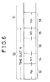
- FIG. 6 shows a frame format for digital data signals used in the present invention.
- the digital data signals are transmitted in successive time slots 50, 51 each composed of N symbols.
- the digital data signals in the time slots 50, 51 include training sequences 52, 53 each composed of Np symbols.
- Each of the digital data signals in the time slots 50, 51 also includes data 54 composed of N1 symbols, data 55 composed of N2 symbols, and data 56 composed of ⁇ N-(N1+N2+Np) ⁇ symbols.
- FIG. 7 shows a system for receiving a digital data signal according to an embodiment of the present invention.
- the system has a memory 201, two channel estimators 202, 203, a channel information generator 204, three adaptive maximum likelihood channel estimators 205, 206, 207, and a demodulated signal generator 208.
- the memory 201 stores all N symbols of a digital data signal to be demodulated which is supplied in one time slot 50 from an input terminal 200, and also Np symbols of the training sequence 53 of a next digital data signal supplied in a next time slot 51.
- Each of the channel estimators 202, 203 extracts channel impulse response from the Np symbols of the training sequence 52 in the time slot 50 and the N1 symbols of the data 54 in the time slot 50, or channel impulse response from the Np symbols of the training sequence 53 in the time slot 51, based on the symbols stored in the memory 201.
- the channel estimators 202, 203 output first and second channel impulse response, respectively, as primary estimated values of channel impulse responses.
- the channel impulse response generator 204 receives the first and second channel impulse response from the channel estimators 202, 203 and generates and outputs third channel impulse response, which is a combination of the first and second channel impulse response, as an estimated value of a channel impulse response for the data 56.
- the adaptive maximum likelihood channel estimators 205, 206, 207 receive the first, second, and third channel impulse response, respectively, from the channel estimators 202, 203 and the channel impulse response generator 204, and also receive the training sequence 52, the data 54, the data 55, or the data 56, and partially equalize and demodulate the digital data signal in the time slot 50.
- the demodulated signal generator 208 combines partially equalized and demodulated signals from the adaptive maximum likelihood channel estimators 205, 206, 207 into a demodulated signal for the time slot 50, and supplies the demodulated signal to an output terminal 209.
- the adaptive maximum likelihood channel estimators 205, 206, 207 may be uniquely constructed given the type of modulation for transmitted signals and the channel impulse response, for example, as shown in J. G. Proakis, Digital Communications, 1983, McGraw-Hill, pp. 394 - 400. Accordingly, the channel impulse response is used as the channel information in the present invention.
- the system in the embodiment shown in FIG. 7 has a plurality of channel estimators and a plurality of adaptive maximum likelihood channel estimators, the system may have only one channel estimator and only one adaptive maximum likelihood channel estimator, and they may perform a plurality of processing operations according to time-division multiplexing.
- adaptive maximum likelihood channel estimators are used as demodulating means in the system shown in FIG. 7, decision-feedback equalizers or linear equalizers may also be used for this purpose.
- FIG. 8 shows a system for receiving a digital data signal according to another embodiment of the present invention.
- the system shown in FIG. 8 is a simplified modification of the system shown in FIG. 7 for receiving digital data signals whose N symbols in each time slot are subject to relatively infrequent variations, and channel impulse response therefore has little estimated error.
- the system has a memory 101 comprising two memories 101A, 101B, two channel estimators 102, 103, a channel information generator 104, and a demodulator 105.
- the memory 101A stores all N symbols of a digital data signal in the time slot 50 supplied from an input terminal 100, and the memory 101B stores Np symbols of the training sequence 53 of a digital data signal in the next time slot 51 supplied from the input terminal 100.
- the channel estimators 102, 103 extract channel impulse response from the Np symbols of the training sequences 52, 53 supplied from the memories 101A, 101B, respectively, and output respective first and second channel impulse response to the channel information generator 104.
- the channel information generator 104 combines the first and second channel impulse response into third channel impulse response as a channel impulse response with respect to the N symbols in the time slot 50, and outputs the third channel impulse response to the demodulator 105.
- the demodulator 105 receives the signal in the time slot 50 from the memory 101A, and equalizes and demodulates the supplied signal with the third channel impulse response from the channel impulse response generator 104.
- the demodulator 105 outputs the demodulated signal to an output terminal 106.
- the channel estimators 202, 203 and 102, 103 may be the same as the conventional channel estimators 72, 82, 1003, 1004 shown in FIGs. 2, 3, and 5. If maximum-period sequences are successively transmitted as training sequences, a system disclosed in EP Patent Laid-Open No. A2-0396101 (K. Okanoue) published Nov. 7, 1990 may also be employed. After being initialized by the information extracted from the training sequence 52, the channel estimator 202 then estimates and outputs a channel impulse response based on the data 54 composed of N1 symbols.
- the channel information generators 204, 104 generate a channel impulse response as third channel information from two, i.e., the first and second, channel impulse response, according to an algorithm which produces an intermediate channel impulse response between the two channel impulse responses according to linear interpolation.
- FIG. 9 shows, by way of example, the manner in which the channel information generator 104 generates third channel impulse response.
- FIG. 9 illustrates a two-wave model including a main wave h 0 and a wave h 1 that is delayed by a one-symbol time Ts with respect to the main wave h 0 .
- channel impulses h 0 (O), h 1 (O) estimated from a training sequence 62 in a time slot 60 are regarded as channel impulses 64 at a time O
- channel impulse responses h 0 (N), h 1 (N) estimated from a training sequence 63 in a time slot 61 are regarded as channel impulses 65 at a time N.
Landscapes
- Engineering & Computer Science (AREA)
- Power Engineering (AREA)
- Computer Networks & Wireless Communication (AREA)
- Signal Processing (AREA)
- Time-Division Multiplex Systems (AREA)
- Cable Transmission Systems, Equalization Of Radio And Reduction Of Echo (AREA)
- Filters That Use Time-Delay Elements (AREA)
- Dc Digital Transmission (AREA)
Claims (4)
- Verfahren zum aufeinanderfolgenden Empfang von digitalen Zeitmultiplex-Datensignalen, die jeweils aus mehreren Symbolen einschließlich einer Trainingssequenz von Symbolen in einem Zeitschlitz bestehen, wobei das Verfahren den folgenden Schritt aufweist:Speichern von empfangenen digitalen Datensignalen , Extrahieren der Kanalimpulsantwort aus den gespeicherten digitalen Datensignalen und Entzerren und Demodulieren aller Symbole des digitalen Datensignals durch die extrahierte Kanalimpulsantwort, gekennzeichnet durch die folgenden Schritte:Speichern von mindestens N Symbolen eines Zeitschlitzes (50, 60) und von Np Symbolen einer Trainingssequenz (53, 63) des folgenden Zeitschlitzes (51, 61) der empfangenen digitalen Datensignale,Extrahieren einer ersten Kanalimpulsantwort (h(O)) aus einem Teil eines gespeicherten, in einem ersten Zeitschlitz (50, 60) empfangenen digitalen Datensignals, wobei der Teil eine Trainingssequenz enthält, und einer zweiten Kanalimpulsantwort ((h(N)) aus einem Teil eines gespeicherten digitalen Datensignals, das in einem auf den ersten Zeitschlitz (50, 60) folgenden zweiten Zeitschlitz (51, 61) empfangen wird, wobei der Teil eine Trainingssequenz enthält,Kombinieren der ersten und zweiten Kanalimpulsantworten zu einem Schätzwert (h(k)) einer Kanalimpulsantwort bezüglich aller Symbole des digitalen Datensignals in dem ersten Zeitschlitz (50, 60), undEntzerren und Demodulieren aller Symbole des digitalen Datensignals in dem ersten Zeitschlitz (50, 60) mit dem Schätzwert einer Kanalimpulsantwort.
- Vorrichtung zum aufeinanderfolgenden Empfang von digitalen Zeitmultiplex-Datensignalen die jeweils aus einer Vielzahl von N Symbolen einschließlich einer Trainingssequenz von Np Symbolen in einem Zeitschlitz bestehen, gekennzeichnet durch:eine Speichereinrichtung (101, 201) zum Speichern von N Symbolen eines in einem ersten Zeitschlitz (50, 60) empfangenen digitalen Datensignals und von mindestens einer Trainingssequenz (53, 63) von Np Symbolen eines digitalen Datensignals, das in einem auf den ersten Zeitschlitz folgenden zweiten Zeitschlitz (51, 61) empfangen wird,eine erste Kanalimpulsantwort-Ausgabeeinrichtung (101A, 202) zum Extrahieren einer ersten Kanalimpulsantwort aus einem Teil des gespeicherten digitalen Datensignals, das eine Trainingssequenz (52, 62) von Np Symbolen im ersten Zeitschlitz (50, 60) aufweist, und zur Ausgabe der ersten Kanalimpulsantwort,eine zweite Kanalimpulsantwort-Ausgabeeinrichtung (101B, 203) zum Extrahieren einer zweiten Kanalimpulsantwort aus einem Teil des gespeicherten digitalen Datensignals, das die Trainingssequenz (53, 63) von Np Symbolen im zweiten Zeitschlitz (51, 61) aufweist, und zur Ausgabe der zweiten Kanalimpulsantwort,eine dritte Kanalimpulsantwort-Ausgabeeinrichtung (104, 204) zum Kombinieren der ersten und der zweiten Kanalimpulsantwort von der ersten und der zweiten Kanalimpulsantwort-Ausgabeeinrichtung (101A, 202, 101B, 203) zu einer dritten Kanalimpulsantwort bezüglich des ersten Zeitschlitzes (50, 60) und zur Ausgabe der dritten Kanalimpulsantwort, undeine Demodulationseinrichtung (105, 208) zum Entzerrern und Demodulieren der N Symbole des digitalen Datensignals im ersten Zeitschlitz (50, 60) mit den ersten bis dritten Kanalimpulsantworten.
- Vorrichtung nach Anspruch 2, wobei die erste Kanalimpulsantwort-Ausgabeeinrichtung (101A, 202) eine Einrichtung zum Extrahieren der ersten Kanalimpulsantwort aus den Np Symbolen der Trainingssequenz (52, 62) und den auf die Np Symbole (52, 62) folgenden N1 Symbolen (54) im ersten Zeitschlitz (50, 60) aufweist, wobei die zweite Kanalimpulsantwort-Ausgabeeinrichtung (101B, 203) eine Einrichtung zum Extrahieren der zweiten Kanalimpulsantwort aus den Np Symbolen der Trainingssequenz (53, 63) im zweiten Zeitschlitz (51, 61) aufweist, und wobei die Demodulationseinrichtung (105, 208) eine Einrichtung zum Entzerren der Trainingssequenz und der N1 Symbole (54) im ersten Zeitschlitz (50, 60) mit der ersten Kanalimpulsantwort, zum Entzerren der letzten N2 Symbole (55) im ersten Zeitschlitz (50, 60) mit der zweiten Kanalimpulsantwort, zum Entzerren der übrigen Symbole (56) mit Ausnahme der Np, N1 und N2 Symbole (52, 54, 55) im ersten Zeitschlitz (50, 60) mit der dritten Kanalimpulsantwort und zum Kombinieren der entzerrten Symbole zur Demodulation und Ausgabe aller Symbole im ersten Zeitschlitz (50, 60) aufweist.
- Vorrichtung nach Anspruch 2, wobei die erste Kanalimpulsantwort-Ausgabeeinrichtung (101A, 202) eine Einrichtung zum Extrahieren der ersten Kanalimpulsantwort aus den Np Symbolen der Trainingssequenz (52, 62) im ersten Zeitschlitz (50, 60) aufweist, wobei die zweite Kanalimpulsantwort-Ausgabeeinrichtung (101B, 203) eine Einrichtung zum Extrahieren der zweiten Kanalimpulsantwort aus den Np Symbolen der Trainingssequenz (53, 63) im zweiten Zeitschlitz (51, 61) aufweist, wobei die dritte Kanalimpulsantwort-Ausgabeeinrichtung (104, 204) eine Einrichtung zum Erzeugen und zur Ausgabe der dritten Kanalimpulsantwort bezüglich aller N Symbole im ersten Zeitschlitz (50, 60) aus den ersten und zweiten Kanalimpulsantworten aufweist, und wobei die Demodulationseinrichtung (105, 208) eine Einrichtung zum Entzerren und Demodulieren aller N Symbole im ersten Zeitschlitz (50, 60) allein mit der dritten Kanalimpulsantwort und zur Ausgabe der entzerrten Symbole aufweist.
Applications Claiming Priority (2)
| Application Number | Priority Date | Filing Date | Title |
|---|---|---|---|
| JP253261/91 | 1991-10-01 | ||
| JP3253261A JP2748743B2 (ja) | 1991-10-01 | 1991-10-01 | データ受信方式 |
Publications (2)
| Publication Number | Publication Date |
|---|---|
| EP0535403A1 EP0535403A1 (de) | 1993-04-07 |
| EP0535403B1 true EP0535403B1 (de) | 1997-04-16 |
Family
ID=17248819
Family Applications (1)
| Application Number | Title | Priority Date | Filing Date |
|---|---|---|---|
| EP92115284A Expired - Lifetime EP0535403B1 (de) | 1991-10-01 | 1992-09-07 | Empfang eines digitalen TDMA-Datensignals mit Kompensation von Kanaländerungen |
Country Status (5)
| Country | Link |
|---|---|
| US (1) | US5303226A (de) |
| EP (1) | EP0535403B1 (de) |
| JP (1) | JP2748743B2 (de) |
| CA (1) | CA2077104C (de) |
| DE (1) | DE69219048T2 (de) |
Families Citing this family (37)
| Publication number | Priority date | Publication date | Assignee | Title |
|---|---|---|---|---|
| US5583886A (en) * | 1992-12-03 | 1996-12-10 | Motorola, Inc. | Method for determining a plurality of channel responses and modifying a received signal therewith |
| FR2700086B1 (fr) * | 1992-12-30 | 1995-04-28 | Alcatel Radiotelephone | Procédé de transmission d'informations à débit élevé par allocation multiple de blocs, procédé de réception associé et dispositif de réception pour sa mise en Óoeuvre. |
| US5414734A (en) * | 1993-01-06 | 1995-05-09 | Glenayre Electronics, Inc. | Compensation for multi-path interference using pilot symbols |
| FI108975B (fi) * | 1993-03-09 | 2002-04-30 | Nokia Corp | Opetusjakso digitaalisessa solukkopuhelinjärjestelmässä |
| DE4311604C1 (de) * | 1993-04-08 | 1994-07-28 | Ant Nachrichtentech | Zuverlässigkeitsgesteuerte Datendetektion in Empfängern für TDMA-Mobilfunksysteme |
| US5502713A (en) * | 1993-12-07 | 1996-03-26 | Telefonaktiebolaget Lm Ericsson | Soft error concealment in a TDMA radio system |
| US5553074A (en) * | 1994-03-04 | 1996-09-03 | Trustees Of Columbia University In The City Of New York | Transmission format in packet based communications |
| US5917853A (en) * | 1994-06-30 | 1999-06-29 | Academy Of Applied Science | Method of and apparatus for training high speed digital telephonic modems to obviate imperfections in the telephone channel, while simultaneously allowing conversation |
| FI102797B (fi) * | 1994-10-07 | 1999-02-15 | Nokia Mobile Phones Ltd | Signaalin ilmaisumenetelmä TDMA-matkaviestinjärjestelmän vastaanottime ssa sekä menetelmän toteuttava vastaanotin |
| SE503522C2 (sv) * | 1994-10-31 | 1996-07-01 | Ericsson Telefon Ab L M | Förfarande och anordning för kanalestimering |
| US5742640A (en) * | 1995-03-07 | 1998-04-21 | Diva Communications, Inc. | Method and apparatus to improve PSTN access to wireless subscribers using a low bit rate system |
| FI101256B1 (fi) * | 1995-10-03 | 1998-05-15 | Nokia Mobile Phones Ltd | Menetelmä vastaanotetun signaalin ajoituksen mittaamiseksi tiedonsiirtojärjestelmässä ja menetelmän toteuttava matkaviestin |
| FI962140A7 (fi) | 1996-05-21 | 1997-11-22 | Nokia Corp | Menetelmä impulssivasteen estimoimiseksi sekä vastaanotin |
| FR2751815B1 (fr) * | 1996-07-24 | 1998-10-02 | Matra Communication | Procede de demodulation numerique d'un segment de signal |
| FR2751811B1 (fr) * | 1996-07-24 | 1998-10-09 | Matra Communication | Procede de demodulation numerique |
| GB2321832B (en) * | 1997-01-30 | 1999-01-06 | Motorola Israel Ltd | Method to train a radio |
| US6243428B1 (en) * | 1997-06-11 | 2001-06-05 | Ericsson Inc. | Method and apparatus for band-adaptive demodulation |
| IT1293447B1 (it) * | 1997-07-14 | 1999-03-01 | Cselt Centro Studi Lab Telecom | Procedimento e sistema per la ricezione di segnali digitali |
| DE19747457C2 (de) | 1997-10-27 | 2000-04-06 | Siemens Ag | Verfahren und Anordnung zur Übertragung von Daten über eine Funkschnittstelle in einem Funk-Kommunikationssystem |
| DE19747369A1 (de) * | 1997-10-27 | 1999-05-06 | Siemens Ag | Übertragungskanalschätzung in Telekommunikationssystemen mit drahtloser Telekommunikation |
| GB9810686D0 (en) * | 1998-05-19 | 1998-07-15 | King S College London | Dual direction estimator |
| US6263030B1 (en) * | 1998-07-01 | 2001-07-17 | Ericsson Inc. | Equalizer with channel tracker switching |
| JP3029031B2 (ja) | 1998-09-03 | 2000-04-04 | 日本電気株式会社 | 内挿同期検波方法と無線通信システム |
| JP3680592B2 (ja) * | 1998-10-30 | 2005-08-10 | 株式会社日立製作所 | 通信装置 |
| JP2001060894A (ja) * | 1999-07-13 | 2001-03-06 | Texas Instr Inc <Ti> | 局通信信号内のユニークなセルビットシーケンスを周期化した無線通信システム |
| US7372825B1 (en) | 1999-07-13 | 2008-05-13 | Texas Instruments Incorporated | Wireless communications system with cycling of unique cell bit sequences in station communications |
| EP1100211A1 (de) | 1999-11-09 | 2001-05-16 | Lucent Technologies Inc. | Filter für ein Telekommunikationssystem |
| US6717985B1 (en) | 2000-03-08 | 2004-04-06 | Telefonaktiebolaget Lm Ericsson (Publ) | Technique for efficiently equalizing a transmission channel in a data transmission system |
| US6870858B1 (en) * | 2000-05-12 | 2005-03-22 | Nokia Corporation | Training sequence based signalling for enhanced general packet radio service (EGPRS) |
| US20020172166A1 (en) * | 2001-03-22 | 2002-11-21 | Huseyin Arslan | Communications system and method for measuring short-term and long-term channel characteristics |
| KR100879942B1 (ko) * | 2002-02-16 | 2009-01-22 | 엘지전자 주식회사 | 채널품질지시자 코딩을 위한 기저수열 생성방법 |
| US7862571B2 (en) * | 2003-07-25 | 2011-01-04 | Microline Surgical, Inc. | Occlusion clip and method of applying same |
| TWI252647B (en) * | 2004-09-03 | 2006-04-01 | Benq Corp | Method for channel estimation |
| WO2008010284A1 (fr) * | 2006-07-20 | 2008-01-24 | Fujitsu Limited | Démodulateur mimo et procédé |
| IL203785A (en) | 2007-09-12 | 2014-07-31 | Qualcomm Inc | Devices to increase capacitance and methods for wireless communication |
| US8781037B2 (en) * | 2012-06-27 | 2014-07-15 | Intel Mobile Communications GmbH | Method and a processing unit for processing a data signal |
| RU2565014C2 (ru) * | 2013-11-19 | 2015-10-10 | Открытое акционерное общество "Камчатский гидрофизический институт" (ОАО "КГФИ") | Способ декодирования сигналов связи |
Family Cites Families (3)
| Publication number | Priority date | Publication date | Assignee | Title |
|---|---|---|---|---|
| US4852090A (en) * | 1987-02-02 | 1989-07-25 | Motorola, Inc. | TDMA communications system with adaptive equalization |
| US5127051A (en) * | 1988-06-13 | 1992-06-30 | Itt Corporation | Adaptive modem for varying communication channel |
| US5047859A (en) * | 1990-10-09 | 1991-09-10 | North American Philips Corporation | Method and apparatus for communication channel identification and signal restoration |
-
1991
- 1991-10-01 JP JP3253261A patent/JP2748743B2/ja not_active Expired - Lifetime
-
1992
- 1992-08-28 CA CA002077104A patent/CA2077104C/en not_active Expired - Fee Related
- 1992-09-07 DE DE69219048T patent/DE69219048T2/de not_active Expired - Fee Related
- 1992-09-07 EP EP92115284A patent/EP0535403B1/de not_active Expired - Lifetime
- 1992-10-01 US US07/955,320 patent/US5303226A/en not_active Expired - Fee Related
Also Published As
| Publication number | Publication date |
|---|---|
| JP2748743B2 (ja) | 1998-05-13 |
| CA2077104A1 (en) | 1993-04-02 |
| US5303226A (en) | 1994-04-12 |
| JPH0595378A (ja) | 1993-04-16 |
| CA2077104C (en) | 1998-08-18 |
| DE69219048D1 (de) | 1997-05-22 |
| DE69219048T2 (de) | 1997-07-24 |
| EP0535403A1 (de) | 1993-04-07 |
Similar Documents
| Publication | Publication Date | Title |
|---|---|---|
| US5303226A (en) | Reception of TDMA digital data signal with compensation for channel variations | |
| AU695989B2 (en) | Method and apparatus for channel estimation | |
| JP4421682B2 (ja) | ディジタル伝送システムにおける受信機のための拡張されたチャンネル推定等化器 | |
| AU637166B2 (en) | Soft decision decoding with channel equalization | |
| US5353307A (en) | Automatic simulcast alignment | |
| US5694437A (en) | Device and method for data signal detection in the presence of distortion and interference in communication systems | |
| JP4555403B2 (ja) | ディジタル伝送装置の受信機のための状態削減シーケンス推定法によるイコライザ | |
| US5285482A (en) | Timing recovery device for receiver installation using adaptive equalization and oversampling associated with differentially coherent demodulation | |
| KR100852012B1 (ko) | Tdma 및/또는 fdma 전송 중 간섭을 제거하는 방법 | |
| EP1016251B1 (de) | Verfahren und einrichtung zur demodulierung von datensymbolen | |
| EP0496677B1 (de) | Adaptive Entzerrer | |
| CN1315100A (zh) | 使用接收信号的多采样定时减小同信道干扰的方法和系统 | |
| WO1995008889B1 (en) | High speed simulcast system using adaptive compensation | |
| US6707850B1 (en) | Decision-feedback equalizer with maximum-likelihood sequence estimation and associated methods | |
| JPH1056406A (ja) | 等化装置における波形等化処理方法 | |
| JP2002232390A (ja) | Ofdm復調装置 | |
| US6292510B1 (en) | Automatic equalization method and automatic equalizer | |
| KR100218671B1 (ko) | 주파수 선택적 레일레이 페이딩 보상 시스템 | |
| Lee et al. | Separation and equalization of cochannel GSM signals | |
| JPH06252810A (ja) | 等化器 |
Legal Events
| Date | Code | Title | Description |
|---|---|---|---|
| PUAI | Public reference made under article 153(3) epc to a published international application that has entered the european phase |
Free format text: ORIGINAL CODE: 0009012 |
|
| 17P | Request for examination filed |
Effective date: 19930120 |
|
| AK | Designated contracting states |
Kind code of ref document: A1 Designated state(s): DE GB SE |
|
| 17Q | First examination report despatched |
Effective date: 19950822 |
|
| GRAG | Despatch of communication of intention to grant |
Free format text: ORIGINAL CODE: EPIDOS AGRA |
|
| GRAH | Despatch of communication of intention to grant a patent |
Free format text: ORIGINAL CODE: EPIDOS IGRA |
|
| GRAH | Despatch of communication of intention to grant a patent |
Free format text: ORIGINAL CODE: EPIDOS IGRA |
|
| GRAA | (expected) grant |
Free format text: ORIGINAL CODE: 0009210 |
|
| AK | Designated contracting states |
Kind code of ref document: B1 Designated state(s): DE GB SE |
|
| REF | Corresponds to: |
Ref document number: 69219048 Country of ref document: DE Date of ref document: 19970522 |
|
| PLBE | No opposition filed within time limit |
Free format text: ORIGINAL CODE: 0009261 |
|
| 26N | No opposition filed | ||
| REG | Reference to a national code |
Ref country code: GB Ref legal event code: IF02 |
|
| PGFP | Annual fee paid to national office [announced via postgrant information from national office to epo] |
Ref country code: GB Payment date: 20020904 Year of fee payment: 11 |
|
| PGFP | Annual fee paid to national office [announced via postgrant information from national office to epo] |
Ref country code: DE Payment date: 20020911 Year of fee payment: 11 |
|
| PGFP | Annual fee paid to national office [announced via postgrant information from national office to epo] |
Ref country code: SE Payment date: 20020919 Year of fee payment: 11 |
|
| PG25 | Lapsed in a contracting state [announced via postgrant information from national office to epo] |
Ref country code: GB Free format text: LAPSE BECAUSE OF NON-PAYMENT OF DUE FEES Effective date: 20030907 |
|
| PG25 | Lapsed in a contracting state [announced via postgrant information from national office to epo] |
Ref country code: SE Free format text: LAPSE BECAUSE OF NON-PAYMENT OF DUE FEES Effective date: 20030908 |
|
| PG25 | Lapsed in a contracting state [announced via postgrant information from national office to epo] |
Ref country code: DE Free format text: LAPSE BECAUSE OF NON-PAYMENT OF DUE FEES Effective date: 20040401 |
|
| GBPC | Gb: european patent ceased through non-payment of renewal fee |
Effective date: 20030907 |
|
| EUG | Se: european patent has lapsed |