EP0533757B1 - Raumklang-prozessor - Google Patents
Raumklang-prozessor Download PDFInfo
- Publication number
- EP0533757B1 EP0533757B1 EP91910951A EP91910951A EP0533757B1 EP 0533757 B1 EP0533757 B1 EP 0533757B1 EP 91910951 A EP91910951 A EP 91910951A EP 91910951 A EP91910951 A EP 91910951A EP 0533757 B1 EP0533757 B1 EP 0533757B1
- Authority
- EP
- European Patent Office
- Prior art keywords
- signals
- signal
- input
- voltage
- amplifier
- Prior art date
- Legal status (The legal status is an assumption and is not a legal conclusion. Google has not performed a legal analysis and makes no representation as to the accuracy of the status listed.)
- Expired - Lifetime
Links
- 239000003990 capacitor Substances 0.000 claims description 83
- 239000011159 matrix material Substances 0.000 claims description 73
- 230000005236 sound signal Effects 0.000 claims description 26
- 230000004044 response Effects 0.000 claims description 22
- 238000001914 filtration Methods 0.000 claims description 12
- 230000008859 change Effects 0.000 claims description 11
- 238000009499 grossing Methods 0.000 claims description 10
- 239000000872 buffer Substances 0.000 claims description 9
- 230000007423 decrease Effects 0.000 claims description 8
- 230000009977 dual effect Effects 0.000 claims description 6
- 230000005669 field effect Effects 0.000 claims description 6
- 238000002156 mixing Methods 0.000 claims description 6
- 230000003139 buffering effect Effects 0.000 claims description 3
- 230000003247 decreasing effect Effects 0.000 claims 2
- 238000012545 processing Methods 0.000 description 27
- 238000010586 diagram Methods 0.000 description 20
- 238000000034 method Methods 0.000 description 17
- 230000000694 effects Effects 0.000 description 16
- 238000000926 separation method Methods 0.000 description 16
- 239000000203 mixture Substances 0.000 description 13
- 230000006870 function Effects 0.000 description 11
- 230000008901 benefit Effects 0.000 description 9
- 230000003750 conditioning effect Effects 0.000 description 9
- 230000009471 action Effects 0.000 description 6
- 230000006872 improvement Effects 0.000 description 4
- 230000001143 conditioned effect Effects 0.000 description 3
- 238000012986 modification Methods 0.000 description 3
- 230000004048 modification Effects 0.000 description 3
- 230000008569 process Effects 0.000 description 3
- 230000002238 attenuated effect Effects 0.000 description 2
- 230000001419 dependent effect Effects 0.000 description 2
- 238000005562 fading Methods 0.000 description 2
- 230000004807 localization Effects 0.000 description 2
- 230000013707 sensory perception of sound Effects 0.000 description 2
- 238000004904 shortening Methods 0.000 description 2
- 238000001228 spectrum Methods 0.000 description 2
- 230000003321 amplification Effects 0.000 description 1
- 230000005540 biological transmission Effects 0.000 description 1
- 239000003985 ceramic capacitor Substances 0.000 description 1
- 230000000295 complement effect Effects 0.000 description 1
- 238000013461 design Methods 0.000 description 1
- 230000006866 deterioration Effects 0.000 description 1
- 238000009434 installation Methods 0.000 description 1
- 238000003199 nucleic acid amplification method Methods 0.000 description 1
- 230000010355 oscillation Effects 0.000 description 1
- 238000005086 pumping Methods 0.000 description 1
- 238000012827 research and development Methods 0.000 description 1
- -1 resistor R23 Substances 0.000 description 1
- 230000029058 respiratory gaseous exchange Effects 0.000 description 1
- 238000005096 rolling process Methods 0.000 description 1
- 230000035945 sensitivity Effects 0.000 description 1
- 238000010561 standard procedure Methods 0.000 description 1
- 238000006467 substitution reaction Methods 0.000 description 1
- 230000009466 transformation Effects 0.000 description 1
- 238000009966 trimming Methods 0.000 description 1
- 230000001755 vocal effect Effects 0.000 description 1
Images







Classifications
-
- H—ELECTRICITY
- H04—ELECTRIC COMMUNICATION TECHNIQUE
- H04S—STEREOPHONIC SYSTEMS
- H04S5/00—Pseudo-stereo systems, e.g. in which additional channel signals are derived from monophonic signals by means of phase shifting, time delay or reverberation
- H04S5/005—Pseudo-stereo systems, e.g. in which additional channel signals are derived from monophonic signals by means of phase shifting, time delay or reverberation of the pseudo five- or more-channel type, e.g. virtual surround
-
- H—ELECTRICITY
- H04—ELECTRIC COMMUNICATION TECHNIQUE
- H04S—STEREOPHONIC SYSTEMS
- H04S3/00—Systems employing more than two channels, e.g. quadraphonic
-
- H—ELECTRICITY
- H04—ELECTRIC COMMUNICATION TECHNIQUE
- H04S—STEREOPHONIC SYSTEMS
- H04S3/00—Systems employing more than two channels, e.g. quadraphonic
- H04S3/02—Systems employing more than two channels, e.g. quadraphonic of the matrix type, i.e. in which input signals are combined algebraically, e.g. after having been phase shifted with respect to each other
-
- H—ELECTRICITY
- H04—ELECTRIC COMMUNICATION TECHNIQUE
- H04S—STEREOPHONIC SYSTEMS
- H04S7/00—Indicating arrangements; Control arrangements, e.g. balance control
- H04S7/30—Control circuits for electronic adaptation of the sound field
- H04S7/307—Frequency adjustment, e.g. tone control
-
- H—ELECTRICITY
- H04—ELECTRIC COMMUNICATION TECHNIQUE
- H04H—BROADCAST COMMUNICATION
- H04H20/00—Arrangements for broadcast or for distribution combined with broadcast
- H04H20/86—Arrangements characterised by the broadcast information itself
- H04H20/88—Stereophonic broadcast systems
- H04H20/89—Stereophonic broadcast systems using three or more audio channels, e.g. triphonic or quadraphonic
Definitions
- the present invention relates in general to processors for the periphonic reproduction of sound. More specifically, the invention relates to an improved variable matrix decoder for multichannel redistribution of audio signals.
- so-called surround processors The basic principle of so-called surround processors is to enhance a two-channel stereophonic source signal so as to drive a multiplicity of loudspeakers arranged to surround the listener, in a manner to provide a high-definition soundfield directly comparable to discrete multitrack sources in perceived performance. An illusion of space may thus be created enabling the listener to experience the fullness, directional quality and aural dimension or "spaciousness" of the original sound environment.
- periphonic reproduction of sound can be distinguished from the operation of conventional soundfield processors which rely on digitally generated time delay of audio signals to simulate reverberation or "ambience" associated with live sound events. These conventional systems do not directionally localize sounds based on information from the original performance space and the resulting reverberation characteristics are noticeably artificial.
- Fixed matrix decoders are those in which a plurality of input signals containing encoded information relating to the directions of sound sources are summed in appropriate proportions and phases to yield a plurality of output signals suitable, after amplification, for driving a corresponding plurality of surrounding loudspeakers in a room, the process being describable in terms of a matrix transformation in which the matrix coefficients are fixed and time-invariant.
- the optimum performance of such decoders occurs when the decoding matrix is the pseudo-inverse of the encoding matrix, and no further improvement in performance is possible unless the coefficients can be varied dynamically.
- Variable matrix decoders also matrix a plurality of encoded input signals to produce a plurality of output signals suitable for driving a multichannel loudspeaker system, but the decoding matrix coefficients do not remain fixed. Instead, they are varied by means of a directionally sensing and control system, which continually monitors the correlations in phase and amplitude ratios between the input signals and adjusts the decoding coefficients to provide the maximum possible enhancement of directional cues for the most prominent sound sources at any instant in time.
- So-called "logic steering" or dynamic separation enhancement techniques typical of variable matrix decoders are described in Scheiber, U.S. Patent No. 3,632,886; Bauer, U.S. Patent No. 3,708,631; Ito and Takahashi, U.S. Patent No.
- control signals and their sum generally behave to provide correct separation, localization and placement of individual predominant sound sources.
- careful attention must also be paid to psychoacoustic performance where the control signals and their corresponding matrix coefficients vary, to ensure a natural perception of sound by the ear-brain combination.
- the resulting presentation can suffer from an anomaly known as "pumping" or "breathing”, since it is clearly obvious when a channel is turned on or off.
- Other audible problems known by those skilled in the art to occur include intermodulation distortion, mislocalization or apparent wandering of sound sources and modulation of noise or rumble associated with the signals.
- attack and decay time constants which are continuously variable over a wide range, and varied in response to both the strength of the individual control signal and the rate of change of the control signals occurring prior to the generation of these time constants.
- the effect would be that audio signal attacks are detected and responded to with very brief periods of shortening of time constants, with longer and smoother time constants restored as soon as the attack demand has been met.
- split-band processing allows for improved audio separation and thus improved directional effects since the separation occurs over a smaller audio signal frequency range, as opposed to being averaged over the entire frequency band.
- the noise and distortion at lower frequencies caused by imperfections in the presentation are also effectively eliminated by band-specific processing techniques.
- known split-band surround processors typically employ a filter network for first receiving input signals in the direct audio path and splitting the signals into high and low-frequency bands, which are then processed by two separate decoders, one for the high and one for the low-frequency band.
- the provision of multiple decoders and associated circuitry complicates these arrangements and adds significantly to their cost.
- the placement of filters in the audio path has a tendency to degrade the audio signal because of the added stages and summing techniques.
- the present invention is directed to an apparatus for the periphonic reproduction of sound on a plurality of loudspeakers derived from audio input signals containing varying directional information said apparatus comprising:
- FIG. 1 there is shown a block diagram of a surround processor 1 embodying features of the present invention having signal input terminals 2 and 4.
- the processor 1 includes an input conditioning and matrix means 6, a variable matrixing means 8 and a servo logic control voltage generator (CVG) 10.
- the input terminals 2 and 4 are connected to the input conditioning and matrix means 6 for receiving left (L) and right (R) channel signals, respectively, from a stereophonic source. It is understood that the left and right signals may or may not be encoded in a conventional manner for surround processing.
- variable matrixing means 8 Six output terminals 12, 14, 16, 18, 20 and 22 are connected to the variable matrixing means 8 for passing directionally enhanced signals processed in accordance with the present invention to respective loudspeakers 24, 26, 28, 30, 32 and 34.
- the loudspeakers 24-34 may be disposed to surround a listener at left front, right front, center front, left back, right back and center back positions, respectively.
- the processed output signals received by the loudspeakers 24-34 are designated by the references LF, RF, CF, LB, RB and CB, respectively.
- the center back (CB) signal path, the output 22 and the loudspeaker 34 are shown in dashed-line form to indicate that they may be omitted, the center back signal derived in the variable matrixing means 8 then being applied equally to the LB and RB signal channels and the loudspeakers 30 and 32, thus producing a "phantom" center back sound image.
- the center front (CF) signal path, the terminal 16 and the loudspeaker 28 may also be omitted, with the CF signal being applied equally to the left front and right front loudspeakers 24 and 26.
- suitable power amplifiers may be applied between the low level output terminals 12-22 and the loudspeakers 24-34, either as a portion of the processor 1 or as one or more separate units, as can be appreciated by those skilled in the art.
- the input conditioning and matrix means 6 conditions the input signals L and R as will be discussed and provides a plurality of combinations of the resulting signals which are designated by the output signal references L', R', -L', and -R' to the variable matrixing means 8 and the CVG 10.
- the input conditioning and matrix means 6 includes at least a pair of inverters and other conditioning and matrixing means.
- the input conditioning may include processing by means of a panorama control to be described later as well as processing by automatic input balancing and other techniques known to those skilled in the art. For this reason, the output signals are shown with primes (') to indicate that the signals L' and R' may differ from the signals L and R.
- the CVG 10 receiving the L' and R' signals conditioned by the matrix means 6 generates control voltage signals labeled Vcf, Vcb, Vcl and Vcr in a manner to be described. These signals are applied to the variable matrixing means 8.
- the bandwidth of the input signals L' and R' from which the control voltages Vcf, Vcb, Vcl and Vcr are derived are limited within the servo logic control voltage generator 10 by means of band-pass filters, as will be described. Further, signals responsive to the ratios of front-to-back information and left-to-right information are derived within the CVG 10, and are then smoothed and conditioned by a special servo logic variable time constant circuit, all as will be described below.
- the variable matrixing means 8 includes fixed and variable gain elements to be described in greater detail for processing the L', R', -L' and -R' signals from the input conditioning and matrix means 6.
- the variable gain elements included in the variable matrixing means 8 are controlled by the externally applied control voltages Vcf, Vcb, Vcl and Vcr for generating the directionally enhanced output signals LF, RF, CF, LB, RB and CB for the respective loudspeakers 24-34.
- Additional outputs for the left side and right side loudspeakers 24, 30 and 26, 32, for example, may also be developed in the variable matrixing means 8.
- One or more subwoofer outputs may also be developed by incorporating an electronic crossover into the means 8 or following it.
- an improved bass equalizer may also be provided, typically for the left front and right front channels. Other modifications as will be apparent to those skilled in the art may also be made.
- the input conditioning and matrix means 6 includes a panorama control 40, a low pass filter block 42 and an input matrix 44.
- the panorama control 40 functions to modify the input signals L and R by application of in-phase or antiphase cross-blending to produce the output signals L' and R' having a wider or narrower stereophonic spread than the input signals L and R.
- the panorama control 40 is optional and is discussed subsequently in detail with reference to FIG. 13.
- the output signals L' and R' from the panorama control 40 are applied to identical low pass filters in the low pass filter block 42 to provide output signals L" and R", which include only the low-frequency components of the signals L' and R'.
- the low pass filters within the block 42 are accurately matched in frequency and phase response.
- the signals L" and R" are subtracted from the L' and R' signals to provide signals containing only the mid- and upper-frequency components of the signals L' and R', for processing by the variable gain elements of the variable matrixing means 8, so that split-band processing may be carried out as will be described.
- the input matrix 44 also contains at least a set of inverting amplifiers (not shown) for providing the -L', -R', -L" and -R" signals and means for combining the signals as required for application to variable gain amplifiers within a voltage controlled amplifier (VCA) block 46 as will be discussed. Since the details of the input matrix 44 are conventional, it will not be described further.
- VCA voltage controlled amplifier
- the variable matrixing means 8 contains the voltage-controlled amplifier (VCA) block 46, an output matrix 48 and a bass equalizer circuit 50.
- the VCA block 46 includes a plurality of voltage-controlled amplifiers each of which is provided with one of the control voltages Vcf, Vcb, Vcl or Vcr, respectively.
- the purpose of the voltage-controlled amplifiers of the VCA block 46 is to provide variable gain paths for their respective input signals, controlled by the aforementioned control voltages, for application of these signals to the output matrix 48, thereby causing variation of the matrixing coefficients in accordance with signal directional information sensed by the CVG 10. As shown in FIG.
- the four control voltages Vcf, Vcb, Vcl and Vcr provide dual-axis control, the front-back axis being provided by Vcf and Vcb, and the left-right axis being provided by Vcl and Vcr. It will be appreciated that in some embodiments of the invention, where single-axis control is required for economy, the control voltages Vcl and Vcr may not be generated and corresponding VCAs will not be provided in the VCA block 46. Equally, it may be appreciated that additional control axes and, hence, control voltages may be provided and corresponding additional VCAs may be included in the VCA block 46.
- the voltage-controlled amplifiers of the block 46 will be described in more detail later, with reference to FIGS. 11 and 12.
- Each of these VCAs typically has summing input circuits for both main and cancellation paths.
- the input matrix 44 may include the summing resistors for these inputs, generating L', R', L' + R', L' - R' signals and combining these subtractively with the corresponding low-frequency signals L", R", L" + R", and L" - R" to produce combined signals containing only mid and upper frequencies, one for each VCA of the block 46.
- the output signals from the VCAs of the VCA block 46 are designated with the references FC, BC, LC and RC, being the signals used for signal-dependent cancellation of front, back, left and right components, respectively, when applied to the output matrix box 48.
- the output matrix 48 receives the signals L', R' and their inverses -L' and -R' from the input matrix 44, and may also receive the signals L" and R" and their inverses, which are combined with the output signals FC, BC, LC and RC, respectively, from the VCA block 46. Accordingly, differing proportions of the direct signals from the input matrix 44 and the cancellation signals from the VCAs of the VCA block 46 are combined in a conventional manner by the output matrix 48 to produce appropriate loudspeaker feed signals, which in the preferred embodiment are the LF, RF, CF, LB, RB and CB signals for the six outputs 12-22, for application by suitable power amplifiers (not shown) to the six loudspeakers 24-34.
- cancellation techniques may be employed such that when a center front (CF) signal would be predominant, the voltage-control signal Vcf will cause signals to be applied to the LF and RF channel loudspeakers 24, 26 to cancel out the signals normally applied thereto by the direct signal paths. Cancellation in the rear loudspeakers may be similarly applied. Also, it will be apparent that a proportion of antiphase blend may be applied in the left and right front loudspeakers 24, 26, which is appropriately cancelled out at the opposite loudspeaker when pure left or right signals are present. As previously mentioned, the number of VCAs in the VCA block 46 may be changed to provide different specific directional characteristics of the input signals for single, dual or multiple axis sensing. According to a feature of the present invention as will be subsequently described, the cancellation techniques will typically be applied only at higher frequencies with the bass frequencies being passed without cancellation.
- the bass equalizer circuit 50 shown in FIG. 2 is typically applied only to the left front and right front channels of the processor 1, but could be applied to any desired channels.
- the purpose of the circuit is to extend the effective frequency range of these two loudspeakers 34, 36 to more effectively reproduce low bass therein, and is especially useful when there is no subwoofer in the system. As mentioned previously, additional subwoofer output may be provided for improved bass response.
- the bass equalizer circuit 56 is discussed subsequently in greater detail.
- the CVG 10 includes a band-pass filter block 52, a log-ratio detector block 54 and a servo logic circuit 56.
- a plurality of band-pass filters are provided in the block 52.
- One or more log-ratio detectors are provided in the block 54 and one or more servo logic circuits in the block 56, for applying variable time constants to output signals from the log-ratio detectors and generating the control signals Vcf, Vcb, Vcl and Vcr.
- the conditioned signals L' and R' received from the panorama control 40 are filtered by matched band-pass filters within the band-pass filter block 52, described in greater detail below with reference to FIG. 10. These filtered signals designated by the references L''', R''' and their inverses -L''' and - R''' are applied to the log-ratio detectors in the log-ratio detector block 54. Typically, only R''' is inverted following the filter, but L''' may also be inverted and in general also applied to the log-ratio detectors as required by a specific embodiment.
- the log-ratio detectors within the block 54 determine or "sense" the ratio of front to back and left to right information contained in the stereo input to the processor 1.
- a log-ratio detector pair within the block 54 receives the inputs L''' + R''' and L'''' - R''' (or R''' - L''') which are derived by means of summing resistors or otherwise and generates signals proportional to the logarithms of the absolute values of these signals.
- signals are smoothed with a short time constant on the order of three milliseconds to eliminate "ripple" from the log-ratio detector circuitry and are differenced to generate a signal corresponding to the logarithm of the ratio of front to back information in the input signals. Strictly, the signals are first differenced, the difference signal then being smoothed, as shown in FIG. 5, where the 3ms time constant is provided by capacitor C105 and resistor R116. But capacitors C103 and C104 also provide some smoothing, and are for the purpose of removing ripple.
- a second log-ratio detector pair within the block 54 receives inputs L''' and R''' and generates a signal corresponding to the logarithm of the ratio between left and right information from the stereo input signals received by the processor.
- the ratios generated by the log-ratio detectors of the block 54 are of the signals as weighted by the filtering and therefore represent these log ratios only for the specific bandwidth in which variable matrix processing will occur. For a typical audio application, this bandwidth is between 200 Hz and 10 kHz, approximately, as shown in FIG. 4.
- the detector outputs from the block 54 are designated by the references Vfb and Vlr and are applied to the servo logic circuit 56, as described in detail later.
- the purpose of the servo logic circuit 56 is to "smooth" the output voltages Vfb and Vlr obtained from the log-ratio detector block 54 and to split these respective voltages each into a pair of control voltages moving in opposite senses for driving the voltage-controlled amplifiers (VCAs) of the block 46.
- VCAs voltage-controlled amplifiers
- the output voltage Vfb is split into the pair of control voltages Vcf and Vcb which move in opposite senses for driving the front and back voltage-controlled amplifiers, respectively.
- the output Vlr is applied to a second servo logic circuit of the block 56 for generating the control voltages Vcl and Vcr which move in opposite senses for driving the left and right VCAs of the block 46, respectively. It is understood that in an alternative embodiment, the output voltage Vlr may be eliminated from the circuitry control voltage generator 16, thus resulting in single axis sensing of the front and back directions only.
- control voltages Vcf, Vcb, Vcl and Vcr operate to vary the gains of the VCAs in the VCA block 46, thereby varying the separation of the audio signals received by the processor 1 dynamically so as to increase the directionally of the sound reproduced by the loudspeakers 24-32.
- control voltages Vcf-Vcr for the VCAs in the VCA block 46 are provided by a detector system which must be preceded by a filter to eliminate low frequencies, since these are not to undergo cancellation.
- this filter should reduce extremely high frequencies since the ear does not use them for direction estimation.
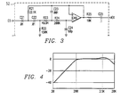
- FIG. 3 illustrates the circuitry for one of typically two filters contained within the band-pass filter block 52 which implements a band-pass characteristic complementary to the Fletcher-Munson curve which relates to the sensitivity of human hearing across the frequency spectrum.
- the circuit comprises a two-pole low-pass network with capacitor C21, resistor R21, capacitor C22 and resistor R22, and a two-pole high pass network, consisting of capacitor C23, resistor R23, capacitor C24 and resistor R24 in cascade, around an op-amp OA6.
- the op-amp OA6 is configured as a voltage follower, and is followed by an additional high-pass pole comprising resistor R25 and capacitor C25, which are connected to a virtual ground input of the following log-ratio detector block 54.
- FIG. 4 illustrates the approximate frequency response characteristic of a filter within the block 52 described above, empirically optimized to yield the values shown in FIG. 3.
- the last pole comprising the resistor R25 and capacitor C25 has not been included in this curve but yields additional low-frequency attenuation.
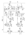
- FIG. 5 there is shown a log-ratio detector circuit contained within the log-ratio detector block 54, it being understood that two of such circuits are to be provided, one for generating the signal Vfb and the other for generating the signal Vlr.
- amplifiers U1A and U1D which may be of industry type TLO84, for example, employ matched diodes U2 in antiparallel arrangement as their feedback impedances, to perform a logarithmic amplifier function.
- the diodes U2 in both the amplifiers U1A and U1D should preferably be closely matched and are typically on the same diode array, which may be an industry type CA3141E, for example.
- the amplifier U1A has inputs L''' and R''' taken from the outputs of the band-pass filter block 52 (FIG. 2).
- the amplifier U1D has inputs L''' and -R''' from the band-pass filter block 52, and is otherwise identical to the amplifier U1A.
- Resistors R101 and R102, and a capacitor C101 form the last time constant of the band-pass filter, functionally equivalent to the resistor R25 and the capacitor C25 discussed previously with reference to FIG. 3 and similarly for the network comprising resistors R103 and R104 and a capacitor C102.
- Amplifiers U1B and U1C with surrounding resistors R105, R106, R107 and R108, form fast inverters.
- the outputs of the amplifiers U1A and U1B pass through a pair of matched diodes U3 to a capacitor C103, which effectively peak-rectify the logarithmic amplifier output with a positive output voltage.
- a resistor R109 serves to bias these matched diodes and forms a discharge path for the capacitor C103.
- the outputs of the amplifiers U1D and U1C are applied to matched diodes U3 and then to a capacitor C104, on which a negative voltage is developed, and a resistor R110 provides a bias for these diodes to the positive supply rail and a discharge path for the capacitor C104.
- the main discharge path for the capacitor C103 is via a resistor R111 and that for the capacitor C104 is via a resistor R112, yielding time constants of about three milliseconds. It is understood that all four of the diodes U2 and U3 form part of a diode array of industry type CA3141E for accurate matching.
- the two output voltages appearing on the capacitors C103 and C104, respectively are proportional to the logarithms of the amplitudes of the L''' +R''' and the L'''' - R'' signals, corresponding to center front and center back components of the stereo inputs to the processor 1.
- the output voltage in such a circuit typically increases by about 60mV for a tenfold increase in current through the diodes, corresponding to a tenfold or 20dB increase in the output current through the capacitor C101 or C102.
- both output voltages should have the same magnitude, but the polarities are opposite, so that the currents through the resistors R111 and R112 cancel out at the input of summing amplifier U4.
- the amplifier U4 is typically supplied from +7.5 V and -6.8 V rails, the latter being dropped from the -7.5 V supply by means of a diode D101 and decoupled by a capacitor C106.
- a limiting function is performed by the amplifier U4, allowing a maximum swing in each direction of approximately 6 volts peak.
- This output swing is achieved for an input voltage difference of about 80 mV, which corresponds to an approximate 21:1 ratio in the input currents applied to the log amplifiers, or approximately 13.3dB.
- a feedback capacitor C105 provides an approximate 3.3 millisecond smoothing time constant around this stage.
- Other op-amps in this quad are used in the servo logic circuit block 56, described subsequently in detail.
- a resistor R115 is an additional feedback resistor which may be electronically switched in parallel with the resistor R116, reducing the detector gain by approximately 36% or 3.8dB for use in some modes of processor operation selected by the function switching controls of the processor 1 (not shown), which apply a control voltage to the input labeled DET.GAIN.
- the output voltage Vfb generated by this circuit is applied to the servo logic circuit of the block 56, and in the circuit shown, goes negative for front signals and positive for back signals.
- a servo logic circuit of the block 56 will now be described with reference to FIGS. 6 and 7.
- the purpose of this circuit is to vary the rate at which the control voltages Vcf, Vcb, Vcl and Vcr respond to changes in predominant signal source direction, while maintaining very smooth operation so that the changes in processor operation are not noticeable to the listener.
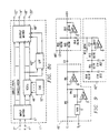
- FIG. 6 shows a simplified schematic of a servo logic circuit of the block 56 for generating the control voltage signals Vcb and Vcf, it being understood that a similar circuit may be contained within the block 56 for generating the control voltages Vcl and Vcr.
- a log-ratio detector output such as Vfb is applied to the input where it is passed into two R-C time constants.
- An upper time constant is formed by resistors R201 and R202 in series, and a capacitor C201.
- a lower time constant is formed by a resistor R203 and a capacitor C202.
- An amplifier A201 is a unity gain buffer, the output of which follows the voltage on the capacitor C201.
- An amplifier A202 is a differential amplifier and receives both the buffered voltage from the capacitor C201 and that on the capacitor C202 and compares these voltages, producing an error voltage at its output.
- This error voltage is rectified by a full-wave rectifier 58 which therefore produces an output proportional to the absolute value of the error.
- This error signal is applied via a resistor R204 to the inverting input of an amplifier A203, which applies and inverts it with gain determined by resistors R205 and R206 in parallel, if a CMOS switch S202 is on, and otherwise by a resistor R205 alone. It is understood that the switch S202 is normally on.
- the resulting output voltage from the amplifier A203 is applied to a PWM oscillator 60, which produces a train of pulses at its output with a duty cycle proportional to the error signal. These pulses are applied to a CMOS switch S201, which short circuits the resistor R201, thereby shortening the upper time constant. This time constant can be varied between 3.5 milliseconds and 50 milliseconds with the component values shown subsequently in FIG. 7.
- the switch S201 When the switch S201 is open, the upper time constant is substantially longer than the lower time constant. When the switch S201 is closed, it is made much shorter, typically shorter than the lower time constant.
- the error voltage produced will be proportional to the rate of change of the input signal Vfb and to the difference between the upper and lower time constants.
- the PWM oscillator For a given rate of change, the PWM oscillator generates a train of pulses of constant width, shorting out the resistor R201 for such a proportion of time that the upper time constant nearly matches the lower one. The faster the rate of change, the closer the matching will become.
- the upper time constant is always longer than the lower one, the response speed of the circuit increases in proportion to the rate of change of the detector output voltage applied to its input.
- the switch S201 At intermediate levels of control, the switch S201 is on for a proportion of time, having the effect of reducing the apparent resistance in series with the capacitor C201 and thereby reducing the upper time constant to some value between the longest and the shortest
- an off-balance detector 62 is provided in the servo logic circuit. Whenever the absolute value of the input signal Vfb exceeds a certain threshold, the off-balance detector 62 switches off a CMOS switch S202, having the effect of increasing the loop gain of the servo logic circuit by raising the gain of the amplifier A203. This enables the circuitry to reach the maximum speed as defined by the resistor R202 and the capacitor C201, while when the switch S202 is off, slower and smoother performance results.
- the switch S202 may be held off by means of a switch S206 (described with reference to FIG. 7) to which an input labeled LOGIC SPEED is applied. This mode is typically used for classical music reproduction.
- the effect of the servo logic circuit just described is twofold.
- the control voltage signal Vfb varies relatively slowly, the time constant applied to it remains long, and the output voltage across the capacitor C201 is varied very smoothly. This voltage becomes the Vcb control voltage after buffering by the amplifier A201.
- the inverter A204 inverts this signal and its output is the voltage-control signal Vcf.
- the servo logic error voltage increases and the upper time constant is forced to match that of the lower R-C network. If the error voltage is large enough, the closeness of this matching is further enhanced by raising the gain of the amplifier A203.
- the PWM oscillator 60 will cease to generate a pulse train and hold the switch S201 on, thereby making the upper time constant that of the resistor R202 and the capacitor C201. It has been found that if this time constant is shorter than the lower time constant, the lower time constant will then dominate the performance of the circuit. Consequently, it is possible to omit the capacitor C202 altogether, and make the resistor R202 and the capacitor C201 determine the minimum time constant instead.
- the servo logic circuit of block 56 thus provides means for smoothing the directional information signals Vfb and Vlr received from the detector block 54 with continuously variable time constants to generate the control voltage signals Vcf-Vcr.
- the circuits are responsive to both the rate of change and amplitude of the detector signals Vfb and Vlr, such that as the difference between the control voltage signals and the detector signals increases, the value of the time constants decreases to permit the control voltage signals to follow closely the detector signals.
- the value of the time constants increases so that variations in the control voltage signals are smooth.
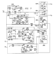
- FIG. 7 there is shown a detailed schematic of the servo logic circuit 56 in a preferred embodiment of the processor 1.
- the voltage Vfb is applied to the resistors R201 and R202 in series, via the switch S203 to the capacitor C201.
- the longest time constant is about 50 milliseconds and the shortest about 3.5 milliseconds.
- the amplifier A201 is one amplifier U6A of a TLO84 quad op-amp, connected as a source follower, which buffers the voltage developed across the capacitor C201.
- the voltage Vfb is also applied to the resistor R203, and then to the capacitor C202, it being understood that the capacitor C202 may be omitted according to the particular embodiment.
- Resistors R203, R207, R208, R209 and amplifier U6D form the differential amplifier A202.
- the effective time constant here is five milliseconds, as the resistors R203 and R207 are effectively in parallel to the capacitor C202. With the capacitor C202 removed, the time constant is then zero, and the maximum speed is determined by the 3.5 millisecond time constant of the resistor R202 and the capacitor C201. Overall, the effective time constant is about five milliseconds, because of the three millisecond time constant of the preceding detector amplifier shown in FIG. 5.
- Amplifier U6C with its associated components forms the full-wave rectifier and is in a standard configuration.
- the resistor R204 transmits a current to amplifier U4C while diode D201 conducts and diode D202 is shut off.
- the amplifier U6C has a unity gain (with a diode drop inside the feedback loop) and drives an opposing current via the resistor R211 which is twice that through the resistor R204, so that on each input polarity the circuit produces a positive input current to the amplifier U4C.
- the output of the amplifier U4C thus goes negative proportionally to the difference between the voltages applied to the amplifier U6D via the resistors R203 and R208, and independently of the sense of the difference.
- a resistor R210 provides offset current compensation for the amplifier U4C, which is typically part of an MC3403 quad op-amp shared with the circuit of FIG. 5. This op-amp U4C is supplied from reduced voltage rails and therefore its output swing is reduced to about +/-6 V.
- the amplifier U4C with its associated resistor R210 equates to the amplifier A203 of FIG. 6, and the resistor R205 with resistor R206 in parallel yields a voltage gain of -0.48 when the switch S202 is on, and this rises to -2.21 when the switch S202 turns off. This is accomplished by the threshold detector 62 as indicated previously.
- the amplifier U4C is a low crossover distortion amplifier such as an industry standard MC3403, and may be in the same package as the amplifier U4 of FIG. 5 in practice, as its output swing is required to be limited because it drives the CMOS switch S202.
- the pulse width modulated (PWM) oscillator 60 is formed from an amplifier U7, which is a TLO84 op-amp, and the associated resistors R212 through R218 and capacitors C203 and C204.
- PWM pulse width modulated
- this circuit When the input voltage goes more negative than the threshold set by the resistors R215 and R216, this circuit begins to oscillate at a rate determined by the capacitor C203 and the effective driving resistance of the resistors R212, R213 and R214 in parallel.
- the duty cycle increases until at a high enough negative input voltage on the capacitor C203 the amplifier output remains positive continuously, keeping the switched S201 turned on.
- the frequency of oscillation is typically well above the audio range, although this is not necessary since the switching signal does not enter the audio signal path.
- the threshold detector circuit 62 comprises two more of the op-amps in the same MC3403 package, U4B and U4D. This package is supplied from reduced voltage rails, so that its output voltage limits are appropriate for driving CMOS switches between +7.5 volts and -7.5 volts supply rails. Resistors R219 and R220 apply the raw control voltage Vfb to capacitors C205 and C206 which are clamped by diodes D203 and D204, respectively. When the voltage at the input of the amplifier U4B is higher than the positive voltage set by resistors R221 and R222, approximately 1.28 volts, the output goes negative, pulling down the input to the switch S202 via diode D205 and thereby increasing the gain of the amplifier U4C.
- This voltage is normally held at +7.5 volts by a resistor R225.
- the output of the amplifier U4D goes negative, pulling down the S202 switch input via diode D206.
- the two clamp diodes D203 and D204 serve an important purpose, in that without them, the capacitors C205 or C206 might be charged to a high voltage in the opposite direction to which they are required to be charged to turn on the appropriate comparator, so that if the control voltage applied changes rapidly from a fully positive state to a fully negative state, a considerable time elapses in which the gain is reduced, because both comparators turn off as the voltage swings through the 2.5 volt window around zero volts.
- the second comparator only has to charge from +0.7 volts to -1.28 volts, reducing its turn-on time by a factor of five. The result is that both comparators may stay on and the logic circuit acts faster.
- the control voltage remains near zero and the loop gain of the servo loop remains low, causing the time constants to remain fairly slow and leading to very smooth decoder action.
- the PWM circuit 60 insures that they are followed with a fastest overall time constant (including the detector time constant) of about five milliseconds, which has been found to give optimum results in conditions of rapidly varying source direction vector.
- the amplifier A204 comprising the amplifier U6B and resistors R226 and R227, inverts the output of the amplifier A201 which is the Vcb control voltage, and thereby generates the control voltage Vcf, which is the other control voltage of this pair.
- Switch S203 is used to turn off the servo logic system by breaking the path through the resistors R201 and R202.
- Switches S204 and S205 are turned on in different user-selected configurations by control means (not shown), and resistors R228 and R229, with capacitors C207, set up some very slow time constants.
- the resistor R208 sets up a twenty-two millisecond time constant with the capacitor C201.
- the resistor R227 and the capacitor C207 set up a 470 millisecond time constant. In these modes, the servo logic is inactive and the processor yields lower dynamic separation but very smooth performance.
- these two logic speeds are used by the Dolby Pro-Logic mode, and the threshold detector 62 is still active, determining when the fast or slow time constants are to be used. If Dolby Pro-Logic is not enabled, both switches stay off. If the logic speed input to the switch S206 is high, the amplifier A203 is switched to high speed and the servo logic stays in the high loop gain mode continuously. However, if Pro-Logic is enabled, the switch S206 is held low and therefore the threshold detector cannot be disabled.
- the threshold detector 62 is also referred to as the off-balance detector in FIG. 6 and as an absolute magnitude comparator, since it compares the signal with a positive voltage in one case and a negative voltage in the other, one or the other comparators pulling down the control terminal of S202 via diodes D205 or D206 if the absolute magnitude of the Vfb control voltage exceeds the threshold voltage.
- a one-shot can be added between the output of the threshold detector 62 and the switch 202, in accordance with Fosgate, U.S. Patent No. 4,932,059, causing the speed up in performance to occur for a limited, defined short period after a short strong center front or back event is detected.
- Fosgate '059 the advantage of such a circuit is to force the control voltages to assume their correct values as soon as possible after sensing a signal attack, while restoring the slower time constants within a period of time short enough to avoid any audible distortion.
- this variation may not be normally be necessary, as the effect of the circuit, of FIG. 7 is already to drive the logic speed to its maximum but only until the voltage on the upper capacitor C201 reaches that on the capacitor C202, which will occur substantially within the time that would be set by such a one-shot.
- FIG. 8B components similar to those previously described will be given the same reference numerals with a prime (') designation, indicating that such represents prior art band splitting arrangements as they would be incorporated into a surround processor 1 of the general form of the present invention as shown in FIG. 8A.
- FIG. 8C the components similar to those previously described will have the same reference numerals with a double prime (") designation, indicating that such represents an alternative embodiment to the processor of the present invention shown in FIG. 2.
- FIG. 8B is a simplified block diagram of a prior art split band processor 1' providing processing only at higher frequencies.
- a conventional input matrix 6' processes the L and R inputs applied to terminals 2' and 4', respectively, to provide direct signals via lines designated DIRECT PATH to an output matrix 48'. It is understood that the input matrix 6' does not include the low-pass filter of the input conditioning and matrix means 6 of the present invention, as shown in FIG. 2.
- Cancellation signals are provided from the input matrix 6' to voltage-controlled amplifiers (VCAs) of block 46'.
- VCAs voltage-controlled amplifiers
- the cancellation signals are varied by signal-dependent control voltages derived from a control voltage generator (CVG) 10'.
- High-pass filters (HPF) within block 47' are placed in series with the VCAs and the block 46' in the cancellation path.
- the output matrix 48' receives the signals from the direct and the cancellation paths and provides output signals to output terminals 12'-20', for application to several amplifiers (not shown) and loudspeakers (as shown in FIGS. 1 and 2).
- the result of placing the high-pass filter block 47' in series with the VCA block 46' cancellation path is that the high-frequency band signals are subtracted out of the full range version of those signals, effectively yielding a low-pass filtered signal.
- the processor 1" includes a low-pass filter block 42" placed in a side chain.
- the outputs from the low-pass filter block 42" are also fed to the output matrix 48".
- the low frequencies are cancelled out in operation of the processor.
- the advantage of using the low-pass filter block 42" over the high-pass filter arrangement of the prior art shown in FIG. 8B, is that the bass frequencies are rolled off more sharply when the signals recombine in the output matrix 48".
- the intention is to process the low frequencies with a fixed matrix, but to pass the upper frequencies through a variable matrix. Cancellation is achieved by subtraction of a signal passed through one of the VCAs from the corresponding signal passed directly to the output matrix 48".
- the low-pass filter and summing circuit 42 of the present invention can be placed ahead of the VCA block 46 and also ahead of the input matrix block 44, as shown in FIG. 2. It is also noted that the filters are typically of the inverting two-pole or three-pole multiple feedback type, three-pole filters being preferred.
- a typical voltage-controlled amplifier of block 46" comprises operational amplifiers OA1 and OA2, and associated components.
- the VCA in block 46" receives an audio signal at terminal E1 and passes it with variable gain to terminal E2. This signal is applied via a resistor R15 to a summing amplifier OA5, which forms part of the output matrix block 48". It is also applied to a resistor R10, with which capacitors C10, C11, C12, resistors R11, R12 and R13, and amplifiers OA4 form a three-pole inverting multiple feedback filter of a standard form known to those skilled in the art.
- a two-pole filter may alternatively be used by omitting the resistor R10 and the capacitor C10 and changing the other component values accordingly.
- the output of the amplifier OA4 is also applied via a resistor R14 to the summing input of an amplifier OA5.
- the two signals via the resistors R15 and R14 are equal and in opposite phase and thus cancel out.
- the output of the amplifier OA4 is negligible, and the signal applied to the amplifier OA5 via the resistor R15 is not cancelled out.
- a third signal is applied via the direct path to an input terminal E3 and then via a resistor R16 to the summing amplifier OA5. Since the VCA shown inverts the signal applied to terminal E1, if the same signal appears at terminal E1 and terminal E3, the result will be that at maximum gain of the VCA, the signals through the resistors R16 and R14 will cancel out, and the output of the summing amplifier OA5, which appears at a terminal E4, will therefore be zero. At low frequencies, however, the cancellation signal via the resistor R15 is itself cancelled out by the signal through the resistor R14, so it can have no effect on the signal passed via the resistor R16, which is therefore only cancelled at mid and upper frequencies.
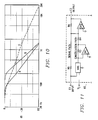
- curve A of FIG. 10 is typical of the attenuation achieved using a two-pole filter, while curve C shows the steeper slope associated with a three-pole filter.
- the cut-off frequencies of these filters may be adjusted for the best audible results, but both filters show attenuation of about 60 decibels at 2 kHz, contrasted with only 30 decibels for the arrangement of FIG. 8B shown by curve B in FIG. 10.
- the components of FIG. 9 may be rearranged so that the high-pass filter comprising the summing amplifier OA4, the resistors R10 through R13 and the capacitors C10 through C12, is driven from the terminal E1 and its output is applied via the resistor R14 to the inverting input of the summing amplifier OA2. Additionally, it would be applied to the variable attenuator network with a second resistor. In this case, the resistor R14 would match the resistor R5, and if the VCA is substantially as shown in FIG. 12, these resistors would be 100K each; and the resistor driving the variable attenuator network would be 200K. The action of this arrangement is to cancel the input to the VCA at low frequencies, while at high frequencies, the VCA behaves normally and its output cancels the signal fed to the summing amplifier OA5 via the terminal E3 and the resistor R16, as previously described.
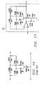
- FIG. 11 wherein a variable gain amplifier circuit according to the present invention is described, forming one of a plurality of such circuits contained within the voltage-controlled amplifier block 46 of FIG. 2.
- a signal voltage applied to an input terminal E1 causes a current to flow through a variable attenuator network (VAN), into the inverting input of an operational amplifier OA1, which is a virtual ground.
- VAN also has a control input designated with the reference VC.
- a feedback resistor R3 determines the voltage which appears at the output of the operation of amplifier OA1. This voltage, which is, of course, inverted relative to that of the terminal E1, is applied via a resistor R4 to the inverting input of a summing amplifier, OA2, which is also a virtual ground. The voltage at the terminal E1 is applied via a resistor R5 to the same point.
- a feedback resistor R6 determines the gain of the amplifier OA2, and hence the output voltage of the amplifier, which appears at a terminal E2.
- the values of the resistors R3 and R4 are chosen such that the current through the resistor R4 is equal and opposite to that through the resistor R4 when the attenuation of the VAN is minimum.
- the output of the amplifier OA2 is nulled.
- the overall gain of the VCA is set by the resistors R5 and R6.
- the output current from the op-amp OA1 via the resistor R4 is subtracted from the direct input current via the resistor R5, and the VGA has an intermediate gain.
- variable attenuation network may be realized with a number of different circuits.
- it may comprise a T-network consisting of two series resistors and a field effect transistor (FET) acting as a voltage-controlled variable resistor shunting their junction to ground, as will be described in FIG. 12.
- FET field effect transistor
- the number of inputs may be expanded to perform signal combining at the VGA input as required for some of the functions detailed below.
- Another method of realizing the attenuator of FIG. 11 may use a two-quadrant multiplier which permits the gain of the amplifier OA1 to vary from zero to some specific maximum value A, where its output through the resistor R4 will cancel the direct input via the resistor R5 to the amplifier OA2.
- FIG. 12 there is depicted a detailed schematic of a VCA according to the present invention.
- the left (L) and the inverted right (-R) signals are each applied to the inverting input of the amplifier OA1 via the resistors R1A and R1B, respectively.
- These resistors may typically have a value of 200K.
- a resistor R2 is typically 1.5K, so that the input voltage is attenuated by about 43 decibels at the junction of the resistors R1A, R1B and R2, when and FET Q1, acting as a variable resistance element, is off. This permits the FET to operate at a low signal voltage for minimum distortion.
- the resistor R3 has a value of 100K in this circuit, and the resistor R4 is 46.4K. If a signal of 1V is applied to either terminal E1A or E1B, corresponding to a pure left or pure right signal at the processor inputs, the output of amplifier OA1 will be 496 mV when FET Q1 is fully cut off. In practice, the potentiometer R9 is adjusted to reduce the gain by about 0.5dB, so the FET Q1 is just turned on. This means that the voltage would be set to about 464 mV at the output of amplifier OA1 under these conditions, so that the current through resistor R4 exactly cancels the current through resistor R5A or R5B.
- the control voltage generator 10 of FIG. 2 will apply the maximum back control voltage to the point labeled Vc, driving the FET Q1 fully on.
- Its minimum resistance is about 330 ohms, typically, so that the current into amplifier OA1 is considerably attenuated, but not completely so.
- the input currents will total 99.8 uA, and of this, about 18 uA will pass through the resistor R2 causing the voltage at the output of the amplifier OA1 to be 180 mV.
- This voltage is applied via the resistor R4 to the inverting input of the amplifier OA2, which is at virtual ground, providing a current of 3.88 uA in antiphase to the total of 20 uA provided through resistors R5A and R5B, so that the net current into the input of amplifier OA2 is 16.12 uA.
- the gain of the amplifier OA2 is adjusted so that its output voltage at terminal E2 is exactly 1V under these conditions, by adjustment of variable resistor R6B, making the total resistance of resistors R6A and R6B about 62K.
- the control path for the FET Q1 comprises operational amplifier OA3, which is a unity-gain buffer, resistors R7 and R8, diode D1 and potentiometer R9.
- the DC voltage at the drain of the FET Q1 is nominally zero, and the AC voltage here is a function of the attenuation produced by the FET Q1.
- This voltage is buffered by the amplifier OA3 and applied to the resistor R7, R8, diode D1 and potentiometer R9.
- the value of the resistor R7 should be equal to the sum of the resistor R8, the AC impedance of diode D1, and the effective impedance of the potentiometer R9.
- the resistor R9 could be 10K, and would be set at its midpoint, yielding an effective resistance of 2.5K.
- the diode current is approximately 75uA, and the effective impedance of the diode is about 400 ohms.
- the resistor R7 is 49.9K
- a suitable value for the resistor R8 is about 3K lower, for example 46.4K, although this value is fairly uncritical.
- the diode D1 is required to avoid forward biasing of the FET Q1 and to compensate for temperature variations.
- the purpose of this resistor chain is to cancel the even-order distortion which would otherwise be introduced by the FET Q1, and to eliminate control voltage feed-through into the audio path and is a standard technique known to those skilled in the art.
- the FET Q1 should have a pinch-off voltage of about -3.5V, for correct operation in this circuit.
- the FET Q1 is typically AC coupled to the junction of resistors R1 and R2, by means of an electrolytic capacitor C1 in parallel with a disc ceramic capacitor C2, which serves to bypass the electrolytic at higher audio frequencies. This prevents offsets from being generated by the control circuitry and passed into the attenuator itself.
- This preprocessor provides a variable panorama control for use with records having varying degrees of left-right separation.
- a fader control is provided to vary the level between front and rear pairs of loudspeakers.
- this fader control is an internal control of the radio or tape source unit.
- An alternative method of control of the surround sound environment is described here as a panorama control and shown in FIG. 13, which corresponds to block 40 of FIG. 2 as indicated by the broken outline.
- a fader control of this type is that in a moving vehicle, FM reception is often subject to "picket-fencing" effects due to rapid fading of the signal as the vehicle passes through regions where standing waves are present through reflections from buildings, mountains, etc.
- this effect is compensated for stereo reception usually by gradually blending the left and right channels down to mono as the signal fades below the desirable minimum level for stereo reception, and then gradually mutes the signal as the signal level falls below the acceptable threshold for monophonic reception.
- the stereophonic signal is wrapped around the listener, and the collapse to monophonic is far more noticeable as it involves a shift of balance towards the front.
- Use of the panorama control in such circumstances can alleviate this effect by reducing the initial separation, if necessary, all the way to monophonic, prior to the processor proper.
- the intermediate range of the panorama control provides an effective front-rear balance control by varying the degree to which the stereo signal is wrapped around the seating position.
- the control is set fully clockwise, the signal again becomes monophonic, but is directed to the rear only. However, this would be of little value in a car, as the difference signal (L-R) is sent to the rear in this case.
- the sound stage can be broadened by this control to undo the effect of reduced separation deliberately introduced in such records. Also, when a record has been produced with inappropriately broad separation, the control can be used to reduce it to an appropriate stage width.
- the panorama control 40 shown in FIG. 2 receives stereo input signals labeled L and R.
- Operational amplifiers A501 and A502 connected as source followers, respectively, buffer these left and right signal inputs.
- the outputs of these amplifiers are applied to the wipers of the dual-ganged panorama control potentiometers R501A and R501B.
- the counterclockwise terminals of these potentiometer elements are connected to terminals identified as LF and RF, respectively, and the clockwise terminals to terminals LB and RB.
- A501 and A502 and the dual potentiometer would be omitted and these four terminals would be driven from the front and rear outputs of the car radio, employing the internal fader therein as the panorama control potentiometer.
- Operational amplifiers A503 and A504 invert the signals appearing at RB and LB terminals respectively, applying their outputs via resistors R506 and R507 to summing amplifiers A505 and A506 respectively.
- the other inputs to A505 are: from terminal LF via resistor R508; from terminal LB via resistor R512; and from terminal RF via resistor R510.
- A506 receives inputs from LF, RF and RB terminals via resistors R511, R509 and R513 respectively. All these resistors have equal values, as do the resistors R502, R504, R503 and R505 which determine the gain and input impedance of inverters A503 and A504.
- amplifier A505 receives the combined signal (LF+RF+LB-RB) and amplifier A506 receives the combined signal (LF+RF+RB-LB).
- equal signals appear at LF and LB, and equal signals are also present at RF and RB.
- the signals applied via resistors R508 and R512 are summed at the inverting input of amplifier A505, while the signal via the resistor R506 cancels that applied via the resistor R510.
- the right channel is thereby cancelled out of amplifier A505 while a unity gain for the left channel is assured by means of the resistor R515 (in the version including amplifiers A501 and A502, and potentiometers R501A and R501B, the value of resistors R515 and R516 may be adjusted to set the overall gain to any desired value).
- the left signal is cancelled from the right channel.
- the left signal will have a gain of 1/2 to the left output L' and the right signal will have a gain of 1/2 to the right output R'.
- Buffer amplifiers A501 and A502 may be made to have a gain of 2 to compensate for this, or resistors R515 and R516 may be made 100K each to increase the gain to unity.
- the left signal is applied as follows: via resistor R508 directly into amplifier A505; via potentiometer R501A into the junction of resistors R512 and R503, half of the current through potentiometer R501A going into each of these resistors.
- the signal at LF will be 1 volt also, and that at LB will be 1/3 volt.
- the output of the left channel L' will be 2/3 volt, and that of the right channel R' will be 1/3 volt, as the signal through the resistor R511 is partially cancelled by that through the resistor R507.
- the right signal of 1 volt appears as 2/3 volt at the right output R' and 1/3 volt at the left output L'. This represents a -6dB blend between the left and right channels.
- the extreme proportion of blend introduced may be changed by choosing the value of dual potentiometer R501A/R501B differently, smaller values giving greater degrees of blend at the extreme positions of the control.
- This position is of benefit when the car is moving through an area of poor FM reception and does not have a manual mono reception switch, as it will alleviate the undesirable phenomenon of "picket-fencing" noise bursts which are particularly offensive when reproduced with a surround-sound system.
- the fader/panorama control As the fader/panorama control is rotated clockwise, the stereo separation will increase, allowing normal stereophonic reception to occur before significant levels are passed to the rear loudspeakers. As the control is further rotated, the normal surround sound presentation will occur at the central position, near which the control will act much like a conventional fader.
- the signals applied to the output amplifiers A505 and A506 will be LB-RB and RB-LB respectively, i.e., the difference of the stereo channels at equal levels in antiphase.
- the decoder will reproduce these in the rear speakers as a monophonic signal, which will, however, have almost complete cancellation of the center front source location, where most vocals are placed in stereophonic music, and a monophonic signal will also be cancelled.
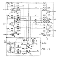
- FIG. 14 shows a variable matrixing means according to the present invention
- this figure also includes certain elements discussed previously, the lower section being identified by the numerals 46, 42 and 44, as this section contains elements of the low-pass filters in block 42, the input matrix block 44 and the voltage controlled amplifiers of block 46 of FIG. 2.
- FIG. 14 In the upper section of FIG. 14 is shown a detailed implementation of the output matrix 48, comprising amplifiers A301 through A306 and associated components therewith.
- variable matrixing means 48 of a surround processor which employs only front-back sensing and control
- the matrix coefficients have been optimized to have 16dB out-of-phase blend between the front channels and 8dB out-of-phase blend in the rear channels. This has proven to give the most satisfactory audible performance with the majority of musical inputs. It helps to reduce center front predominance when there is no significant logic action occurring. In the quiescent state of the logic, as will be explained below, a small residual level of attenuation is provided in the front VCA 74 to provide this blend in the front channels.
- the left and right audio signals are applied to terminals L' and R' respectively.
- Two resistors of typically 200K feed the input summing junction of a two-pole low-pass filter 70 somewhat like that shown in FIG. 9, corresponding with R11 of FIG. 9.
- R10 and C10 of FIG. 9 are not used in the two-pole filter.
- the output of this filter is inverted by inverter 72, corresponding with OA4 in FIG. 9, but the functions of low-pass filtering and inversion are combined in the circuit of FIG. 9 and shown separately here for clarity.
- the output signal of inverter 70 is -0.5(L"+R") being equivalent to summing the outputs of low-pass filters in left and right channels and containing low frequencies only.
- Resistors of 100K each couple left and right inputs into the summing junction of the VCA labeled 74, which receives the front control signal Vcf.
- Another resistor of typically 61.9K, couples the low-pass filtered signal from inverter 72 into this junction, partially cancelling the L'+R' input into this point at low frequencies. If the value of this resistor were 49.9K, this cancellation would be complete, but with the value shown, the low-frequency component is -0.81(L'+R'), so that the net input to this VCA is 0.19(L'+R') at low frequencies, about 15 dB less than at midrange and upper frequencies.
- the filter characteristic used has a slight gain at frequencies just below its cutoff frequency so that the cancellation is complete in this region. This particular configuration of the filter achieves a higher initial slope than for a maximally-flat two-pole filter, although the latter characteristic can also be used and the resistor values adjusted appropriately, as will be apparent to those skilled in the art.
- VCA 74 labeled FC
- This VCA is of the type shown in FIG. 12, but has inputs from L', R' and the low-pass filter 72 as discussed above.
- the three resistors just discussed correspond with R5A, R5B and a third resistor R5C, of 61.9K, not shown in FIG. 12, for the low-pass filter input.
- R1A and R1B there is also a third resistor R1C, of 124K, from the low-pass filter input to the junction of resistors R1A and R1B in this VCA.
- resistor R4 is comprised of a fixed resistor of 56.2K in series with a 10K variable resistor
- the resistor R6A has a value of 52.3K
- the variable resistor R6B is 10K.
- variable resistor R6B is adjusted for complete cancellation of front signal in the left (LF) and right front (RF) outputs when equal in-phase signals are applied to L and R inputs of the decoder; then with a signal applied to L or R only (the detector and both front and back control voltage outputs being zero in this condition) the position of potentiometer R9 is set so that the attenuation of signal through amplifier OA1 is about 0.5dB below the minimum attenuation (the FET Q1 being just turned on) and the value of resistor R4 has been chosen or made adjustable so that the signal at terminal E2 is not quite fully cancelled out.
- the amount of residual signal is chosen to provide the antiphase cross-blending referred to earlier in the LF and RF output channels of the variable matrixing means 48.
- Inputs L' and R' are also applied to inverters 84 and 82 respectively, their output signals being labeled -L' and -R', respectively.
- the L' and -R' signals are applied via two 100K resistors to a VCA labeled 76, which receives the back control voltage Vcb.
- This VCA is substantially as shown in FIG. 12, these resistors being identified with R5A and R5B of FIG. 4.
- the output of VCA 76 is the back cancellation signal labeled BC.
- This is coupled to low-pass filter 78, of similar type to filter 70, and inverter 80, these two components once again comprising an inverting two-pole filter of the type shown in FIG. 9, omitting resistor R10 and capacitor C10.
- resistors R11, R12, R13 all 100K
- capacitor C11, 68 nF capacitor C12, 6.8 nF.
- Other variations of these filter values which will provide the same frequency response can by achieved by multiplying all the resistor values by a constant and dividing the capacitors by the same constant, while varying the resistors or capacitors only will adjust the cut-off frequency, as will be apparent to those skilled in the art. It is important to match the two filter characteristics, however, so that typically these resistors are of 1% tolerance and the capacitors are matched to better than 2%.
- Amplifier A301 receives the L', FC, BC and -BLF signals through resistors of typically 42.2K each. It corresponds in effect to amplifier OA5 of FIG. 6. In this amplifier, the sum of L', FC, BC and -BLF is generated.
- the feedback resistor of typical value 49.9K, provides negative feedback around A301, setting the voltage gain to -1.182 for each of these components.
- the front VCA as having a signal input of 0.5(L'+R'-0.81(L"+R") and a gain kf which varies from 0.308 to 1.
- the back VCA has an input of 0.5(L'-R'), but its gain kb varies from 0 to 1.
- the back VCA output passes through the low-pass filter 78 and inverter 80, as previously mentioned, so that this filter output is 0.405 kb (L"-R").
- amplifier A302 receives the signals R' and FC to its inverting input and signals BC and -BLF via 42.2K resistors to its noninverting input, with a feedback resistor of 49.9K as for the LF channel.
- the balancing resistor from the noninverting input to ground is chosen so that the noninverting input voltage gain will also be 1.182, and has a value of 49.9K for this reason.
- the circuitry surrounding amplifier A303 provides an output labeled CF for application to a center front loudspeaker.
- This amplifier receives input signals L' and R' via 110K resistors to its inverting input, and signal FC via a 49.9K resistor and the parallel network comprising a 4.99K resistor and a 0.0018 uF capacitor in series to its noninverting input.
- the feedback resistor is 49.9K as before.
- the feedback loop also includes a series RC network comprising a 39.2K resistor and a 680 pF capacitor in parallel with this resistor. This has the effect of rolling off the high-frequency portion of the spectrum.
- the voltage gain of amplifier A303 is reduced by about 7dB relative to mid frequencies.
- its voltage gain to L' or R' is 0.454, or about -7dB, and at high frequencies its voltage gain is 0.2.
- the mid-frequency voltage gain of amplifier A303 to the FC signal is 0.625, but this rises to 1.179 at high frequencies.
- Amplifier A304 with its components provides the left back signal LB.
- This amplifier receives input signal L' via a resistor of 56.2K, signal -R' via a 215K resistor and signal FC via 76.8K resistor, to its inverting input. It receives signal BC via an network comprising a 110K resistor in parallel with a 39.2K resistor and a 470pF capacitor in series.
- the -BLF signal is not provided to this point, so that back enhancement operates down to low frequencies.
- the feedback network includes a roll-off at high frequencies, provided by an 82K resistor and a 270pF capacitor in series, in parallel with a 49.9K feedback resistor.
- the balancing resistor at the inverting input is 22.1K.
- this amplifier has a voltage gain of -0.889 to L', -0.232 to -R', and -0.665 to FC. It also has a voltage gain of 0.466 to signal BC.
- This yields the LB signal as: LBmid -0.889(L'-0.261R') + 0.332 kf (L'+R'-0.81(L"+R")) -0.233 kb (L'-R')
- LBmid -0.787(L' + 0.334R' - 0.083(L"+R"
- the RB channel amplifier OA5 receives signal R' via a 56.2K resistor, signal -L' via a 215K resistor, signal FC via a 76.8K resistor, and a signal BC via a 110K resistor and the series network comprising a 49.9K resistor and a 470pF capacitor.
- the feedback network again comprises a 49.9K resistor, in parallel with the series network of an 82K resistor and a 270pF capacitor.
- the mid-frequency voltage gains of this amplifier are -0.889 to signal R', -0.232 to signal -L' and -0.665 to signal FC, and the voltage gain to signal BC is -0.454.
- Amplifier A306 of FIG. 14 with its associated components generates the center back feed signal CB.
- This amplifier receives signal R' via a 100K resistor, signal -L' via a 100K resistor and signal BC via a 121K resistor and the series RC network comprising a 59K resistor and a 390pF capacitor, with feedback again provided by a 49.9K resistor in parallel with the series RC network of an 82K resistor and a 270pF capacitor.
- the voltage gain of amplifier A306 to signals -L' and R' is -0.501, and to signal BC is -0.416 at mid frequencies. At high frequencies, the voltage gains change to -0.31 and -0.784, respectively.
- the signal is predominantly front, however, high frequencies are rolled off, as in the other back channels. The roll-off in these back channels helps to reduce dialog breakthrough into the rear, especially the high-frequency sibilant sounds.
- the matrix of FIG. 14 really provides three-band processing, as the high-frequency region uses different matrixing from the mid-frequency region, and the low-frequency region uses very little logic-derived processing at all. There is a little, only because the FC signal does not completely cancel out at bass frequencies.
- FIG. 15 shows a second embodiment of the variable matrixing means suitable for use with the extended control voltage generator which produces all four of the control signals shown in FIG. 1 and FIG. 2.
- FIG. 15 which describes the midrange processing only, the circuitry is generally similar to that of FIG. 14, but the op-amps have been shown as summing networks with the coefficients indicated, and the active processing includes four VCA circuits instead of two.
- the VCA block 46 and output matrix block 48 and a portion of the input matrix block 44 are indicated by broken outlines. Because some matrixing functions are switched in this processor depending on user-selected options, where negative coefficients are implemented, this is usually done by means of an inverter amplifier, and all of the summation of signals is then done in inverting summing amplifiers configured generally like A301 in FIG. 14.
- inputs L' and R' receive left and right signals, which are inverted by inverting amplifiers 84 and 82, respectively.
- the outputs from these amplifiers, labeled -L' and -R', are processed by VCAs labeled 86 and 88 respectively, which receive and are controlled by control signals Vcl and Vcr, respectively.
- VCAs labeled 86 and 88 receive and are controlled by control signals Vcl and Vcr, respectively.
- two 100K resistors sum L' and R' signals into the input of center front VCA labeled 74, and two 100K resistors sum L' and -R' into the back VCA labeled 76.
- these two VCAs are controlled by control signals Vcf and Vcb respectively.
- Vcl and Vcr are derived from additional detector circuitry similar to that shown in FIGS. 5-7. It will be apparent to those skilled in the art how these circuits are constructed, and therefore no corresponding figure has been included here to demonstrate this aspect of the invention.
- FIG. 14 The low-frequency components of FIG. 14 have been omitted from FIG. 15, but in a practical application, the low-pass filters and inverters would also be present in the circuitry for the reasons stated previously. In this case, the bass filtering is done before the VCAs as indicated in FIG. 2.
- summing amplifiers of FIG. 15 shown as boxes 90 through 100, which correspond respectively with amplifiers A301 through A306 of FIG. 14 and their associated components, only mid-frequency coefficients are shown.
- a difference between FIG. 15 and FIG. 14 is that in the circuit of FIG. 15, both kf and kb are set to zero in the quiescent state, and the out-of-phase blend is therefore provided explicitly by adding 0.16 of -R' to L' at the input of the LF summing amplifier in block 90 and similarly adding 0.16 of -L' to R' in the RF summing amplifier input of block 92. These are cancelled out by tne cancellation signals from VCAs 86 and 88 as required by the left-right sensing circuitry.
- the back VCA 76 has an output of -0.5kb (L'-R') in this embodiment of the processor (resistors in the detailed VCA circuit of FIG. 12. being optimized for this condition). Since the main inputs to LF processing block 90 with this signal total 1.16, the coefficient of 1.16 for signal BC effectively cancels this signal out. For the RF processing block 92, the corresponding BC coefficient has to be -1.16. Similarly, a coefficient of 0.84 for the FC signal out of the front VCA 74, which is -0.5 kf (L'+R'), causes it to cancel in the LF processing circuit 90. The corresponding coefficient in the RF processor 92 is also 0.84. It should be noted that unlike FIG. 14, kf for this embodiment varies from 0 to 1.
- LFmid L' - 0.16R' + 0.16 kr R' - 0.58 kb (L'-R') - 0.42 kf (L'+R')
- RFmid R' - 0.16L' + 0.16 kl L' + 0.58 kb (L'-R') - 0.42 kf (L'+R')
- the center front output and loudspeaker can be switched out of circuit in some embodiments of this surround processor, in which case the cancellation of the FC signal in the left front and right front summing blocks 90 and 92 would be turned off by means of a switch.
- the CF processing in block 94 adds 0.5(L'+R') and then cancels out the L' or R' signal component when it is predominant in the mix by adding -0.5 kl L' and -0.5 kr R'.
- the front signal FC is added in at an increased level, whenever CF is predominant, by adding -0.41 FC, since FC is an inverted output -0.5 kf (L' + R'). This provides a 3dB gain increase for a center front signal, to compensate for its cancellation out of the left front and right front outputs.
- Both channels receive equal proportions of the L' and -R' or -L' and R' signals, so that front dialog is automatically cancelled without an FC cancellation signal being required.
- L' signal alone the -R' signal applied to block 96 is cancelled out, and when R' alone is present, the -L' signal is cancelled in the block 98, so that the opposing channel is removed from the speaker in each case.
- the center back channel processor in block 100 comprises L' and -R' inputs, and a cancellation path from each of the L' and R' signals which cancels out the L' signal when it predominates and vice versa.
- FIG. 17 An improved bass equalizer circuit 50 according to another aspect of the invention is shown in FIG. 17. This employs a twin-T network in the feedback loop of an operational amplifier. The purpose of this equalizer is to improve the apparent low-frequency response of the surround processor when used with loudspeakers of types not having extended low-frequency response.
- FIG. 16 shows a twin-T network according to the applicant's prior art Patent No. 3,883,832, which may, as stated in that patent, be applied in the feedback loop of an operational amplifier to provide a variable bass boost at an adjustable center frequency.
- the twin-T network comprises capacitors C401, C402, C403 and resistors R401, R402 and R403, in a standard configuration known to those skilled in the art.
- Potentiometer R404 varies both the center frequency and the notch depth simultaneously, or when applied in the feedback loop of an operational amplifier R404 varies the center frequency and the amount of bass boost.
- an identical twin-T network comprising resistors R401, R402 and R403 and capacitors C401, C402 and C403 is placed in the feedback loop of an amplifier A401, but instead of using a simple variable resistor as in FIG. 16 to vary the degree of boost and the center frequency, the improved circuit uses a potentiometer R404 from the output of operational amplifier A401 to ground, with a linearizing resistor R406 across the lower section, the wiper of potentiometer R404 being connected via a third resistor R405, to the shunt arm of the twin-T network.
- This circuit applies to block 50 of FIG. 2 as indicated by the broken outline.
- the bass equalizer according to this invention is typically applied to left front and right front outputs, employing a dual-ganged potentiometer, as shown in FIG. 2. It could also be applied to more channels, using a multiple-ganged potentiometer with an appropriate number of sections.
Landscapes
- Physics & Mathematics (AREA)
- Engineering & Computer Science (AREA)
- Acoustics & Sound (AREA)
- Signal Processing (AREA)
- Mathematical Analysis (AREA)
- General Physics & Mathematics (AREA)
- Algebra (AREA)
- Mathematical Optimization (AREA)
- Mathematical Physics (AREA)
- Pure & Applied Mathematics (AREA)
- Theoretical Computer Science (AREA)
- Stereophonic System (AREA)
- Amplifiers (AREA)
- Tone Control, Compression And Expansion, Limiting Amplitude (AREA)
Claims (43)
- Einrichtung zur an mehreren Lautsprechern (24-32) erfolgenden periphonischen Tonwiedergabe, die aus Audio-Eingangssignalen (L, R) gewonnen wird, die veränderliche Richtungsinformationen enthalten, wobei diese Einrichtung umfaßt:ein Eingangsmatrixmittel (6) zum Beschaffen einer Vielzahl von Kombinationssignalen (L'-L'; R'-R') aus den Eingangssignalen (L, R);ein auf ein oder mehrere Steuerspannungssignale (Vcf, Vcr) ansprechendes, variables Matrizierungsmittel (8) zur Matrixdecodierung der Kombinationssignale, um eine Vielzahl von Ausgangssignalen (LF CF RF - LB CB RC) entsprechend der Anzahl von Lautsprechern für die Tonwiedergabe zu erzeugen, wobei die Kombinationssignale mit festen (L'-L'; R'-R') und veränderlichen Anteilen rekombiniert werden, wobei die veränderlichen Anteile in Reaktion auf die Steuerspannungssignale (Vcf---Vcr) verändert werden;ein Detektormittel (54) zum Beschaffen eines oder mehrerer Richtungsinformationssignale (Vfb, Vlr) aus den Eingangssignalen (L, R); undein Mittel (56) zur Erzeugung des einen oder der diversen Steuerspannungssignale (Vcf---Vcr) und zur Glättung des Richtungsinformationssignals (Vfb, Vlr) mit fortlaufend variablen Zeitkonstanten (R201, R202, C201), um das eine oder die diversen Steuerspannungssignale (Vcf---Vcr) zu erzeugen, wobei dieses Mittel (56) sowohl auf die Änderungsrate als auch auf die Amplitude des Richtungsinformationssignal anspricht, so daß in dem Maße, wie der Unterschied zwischen dem Steuerspannungssignal und dem Richtungsinformationssignal ansteigt, der Wert der variablen Zeitkonstanten abnimmt, um es den Steuerspannungssignalen zu ermöglichen, den Richtungsinformationssignalen unmittelbar zu folgen, und in dem Maße, wie der Unterschied zwischen den Steuerspannungssignalen und den Richtungsinformationssignalen abnimmt, der Wert der variablen Zeitkonstanten anwächst, so daß die Änderungen bei den Steuerspannungssignalen gleichmäßig sind.
- Einrichtung nach Anspruch 1, bei der für jedes Richtungsinformationssignal das Glättungsmittel (56) umfaßt:ein variables Tiefpaßfiltermittel (R201, S201, R202, C201) zur Erzeugung einer variablen Zeitkonstante zur Glättung des Richtungsinformationssignals, um eines der Steuerspannungssignale zu beschaffen;ein Differentialverstärkermittel (A202) zum Vergleichen des Ausgangssignals des variablen Tiefpaßfiltermittels (R201, R202, S201, C201) mit dem Richtungsinformationssignal (Vfb, Vlr) und zum Erzeugen eines der Differenz zwischen diesen proportionalen Differenzsignals;ein mit dem Ausgang des Differentialverstärkermittels (A202) verbundenes Absolutwertmittel (58) zur Erzeugung eines zum Absolutwert des Differenzsignals proportionalen Absolutwertsignals; undein zweites Verstärkermittel (A203) zur Verwendung des Absolutwertsignals aus dem Absolutwertmittel (58) zum Steuern des variablen Tiefpaßfiltermittels (R201, R202, C201) zum Abnehmen der Zeitkonstante, wenn das Absolutwertsignal (aus A202) anwächst, und zum Anwachsen der Zeitkonstante, wenn das Absolutwertsignal abnimmt.
- Einrichtung nach Anspruch 2, die darüber hinaus für jedes Richtungsinformationssignal (Vfb, Vlr) einen Absolutgröβenvergleicher (A202) zum Vergleichen des Richtungsinformationssignals mit einer festen Bezugsspannung (Vfb) und zum Steigern der Verstärkung des zweiten Verstärkermittels (A203) immer dann, wenn die Größe des Richtungsinformationssignals die Bezugsspannung übersteigt, wobei dann die Schleifenverstärkung des Glättungsmittels zunimmt, enthält.
- Einrichtung nach Anspruch 2, bei der jedes der variablen Tiefpaßmittel umfaßt:erste und zweite Widerstände (R201, R202), die in Reihe zu einem Kondensator (C201) geschaltet sind, zur Erzeugung einer Zeitkonstanten und zur Verwendung dieser Zeitkonstanten beim Richtungsinformationssignal (Vfb);ein Trennverstärkermittel (A201) zum Zwischenspeichern der Spannung im Kondensator (C201) zum Beschaffen eines der Steuerspannungssignale (Vcf-Vcr);ein elektronisches Schaltmittel (S201), das zum ersten (R201) oder zweiten (R202) der Widerstände zum zeitweiligen Überbrücken dieses einen Widerstandes (R201) parallelgeschaltet ist, so daß, wenn das Schaltmittel (S201) aktiv ist, dieser eine Widerstand überbrückt ist und die Zeitkonstante relativ kurz ist, und wenn das Schaltmittel (S201) inaktiv ist, dieser eine Widerstand nicht überbrückt ist und die Zeitkonstante relativ lang ist; undein pulsdauermoduliertes Oszillatormittel (60) zum Treiben des Schaltmittels zwischen dem aktiven und inaktiven Zustand, so daß der Arbeitszyklus des pulsdauermodulierten Oszillatormittels (60) geändert werden kann, um den Zeitanteil, während dem das Schaltmittel aktiv ist, zu ändern, wobei dann der Wert der Zeitkonstante verändert wird.
- Einrichtung nach Anspruch 3, bei der das zweite Verstärkermittel (A203) wenigstens zwei alternative Verstärkungswerte hat, die mittels eines elektronischen Schaltmittels (S202) ausgewählt werden, das durch das Absolutgrößenvergleichermittel (A202) gesteuert ist.
- Einrichtung nach Anspruch 2, bei der außerdem ein oder mehrere Umkehrverstärker (A204) zum Invertieren eines oder mehrerer der Steuerspannungssignale (Vcf-Vcr) vorgesehen sind, um invertierte Steuerspannungsausgangssignale zu erstellen, die sich in entgegengesetzter Richtung zu den Steuerspannungssignalen (Vcf-Vcr) ändern.
- Einrichtung nach Anspruch 6, bei der die Richtungsinformationen, die in den Audioeingangssignalen entsprechend dem Steuerspannungssignal (Vcf-Vcr) und dem invertierten Steuerspannungssignal (A204) enthalten sind, für Mitte-Hinten (Vcb) bzw. für Mitte-Vorne (Vcf) sind.
- Einrichtung nach Anspruch 6, bei der die Richtungsinformationen (Vfb, Vlr), die im Audioeingangssignal (2, 4) entsprechend dem Steuerspannungssignal (Vcf-Vcr) und dem invertierten Steuerspannungssignal (A204) enthalten sind, für rechts bzw. links sind (Vcl, Vcr), wobei sie von der Servologikschaltung (56) zu den spannungsgesteuerten Verstärkern (46) Anschluß haben.
- Einrichtung nach Anspruch 3, bei der das Absolutgrößenvergleichermittel Schaltungsmittel (R203, C202) einschließt, die dessen Ausgangssignal an einem Umschalten der Verstärkung des zweiten Verstärkermittels (A203) auf einen verringerten Wert hindern, wenn das daran angelegte Richtungsinformationssignal (Vfb, Vlr) von einem großen positiven Wert auf einen großen negativen Wert oder umgekehrt in einer relativ kurzen Zeit wechselt, es jedoch der Verstärkung des zweiten Verstärkermittels (A203) ermöglichen, auf einen niedrigeren Wert vermindert zu werden, wenn sich das Richtungsinformationssignal (Vfb, Vlr) zwischen relativ kleineren Absolutgrößen, die größer als das Festbezugs-Steuersignal ist, ändert.
- Einrichtung nach Anspruch 1, bei der das Glättungsmittel (56) für jedes Richtungsinformationssignal umfaßt:ein variables Tiefpaßfiltermittel (R201, R202, C201) zur Erzeugung einer variablen Zeitkonstanten zum Glätten des Richtungsinformationssignals, um eines der Steuerspannungssignale zu beschaffen;ein Festzeitkonstantenmittel (R203, C202) zur Erzeugung einer festen Zeitkonstanten zum Glätten des Richtungsinformationssignals;ein Differentialverstärkermittel (A202) zum Vergleichen der Ausgangssignale des variablen Tiefpaßfiltermittels und des Festzeitkonstantenmittels und zur Erzeugung eines Differenzsignals, das proportional zu deren Differenz ist;ein Absolutwertmittel (58) zum Erzeugen eines Absolutwertsignals, das proportional zum Absolutwert des Differenzsignals ist; undein zweites Verstärkermittel (A203) zur Verwendung des Absolutwertsignals aus dem Absolutwertmittel (58), um das variable Tiefpaßfiltermittel so zu steuern, daß die Zeitkonstante abnimmt, wenn das Absolutwertsignal zunimmt, und die Zeitkonstante zunimmt, wenn das Absolutwertsignal abnimmt.
- Einrichtung nach Anspruch 1, bei der das Detektormittel (54) eine oder mehrere Log-Ratiodetektorschaltungen (Fig. 5) enthält.
- Einrichtung nach Anspruch 1, die außerdem einen Autobalancemittelblock (6) zur automatischen Balanceeinstellung der Audioeingangssignale enthält.
- Einrichtung nach Anspruch 1, der weiter umfaßt:
ein Bandtrennmittel (42, 48, R14), das Niederfrequenzkomponenten des Audioeingangssignals an einem Durchlaufen durch einen Löschpfad hindert, in dem die Kombinationssignale mit veränderlichen Anteilen rekombiniert werden, wobei die Bandtrennmittel eine Vielzahl von Tiefpaßfiltermitteln (42) mit Eingängen (40) und Ausgängen (48) zum Durchgang eines definierten Bandes niedriger Frequenzen und eine entsprechende Vielzahl von Subtraktionsmitteln (47') einschließen, die jeweils Eingänge und einen Ausgang zum Subtrahieren des Ausgangssignals des Tiefpaßfiltermittels (42) von dessen Eingangssignal haben, um an seinem Ausgang ein entsprechendes Signal zur Verfügung zu stellen, bei dem Niederfrequenzkomponenten entfernt sind. - Einrichtung nach Anspruch 13, das außerdem ein Bandpaßfiltermittel (52) zum Durchgang lediglich von Mittelfrequenzkomponenten des Audioeingangssignals zum Mittel (56) zur Erzeugung der Steuerspannungssignale enthält.
- Einrichtung nach Anspruch 13, bei der die Ausgangssignale aus den Tiefpaßfiltermitteln (42) auch über die Kombinationssignale (44) kombiniert werden, die in festen Anteilen aus einem direkten Signalpfad (L, R) im variablen Matrizierungsmittel rekombiniert (48) werden, so daß ein Teil der tiefpaßgefilterten Signale von einem oder mehreren der Lautsprechersignale subtrahiert wird.
- Einrichtung nach Anspruch 13, bei der das Subtraktionsmittel im Eingangsmatrixmittel (44) enthalten ist.
- Einrichtung nach Anspruch 13, bei der das Subtraktionsmittel im variablen Matrizierungsmittel (8) enthalten ist.
- Einrichtung nach Anspruch 13, bei der das variable Matrizierungsmittel (8) eine Vielzahl spannungsgesteuerter Verstärker (46) entsprechend der Anzahl der Steuerspannungssignale und eine Vielzahl von Summierverstärkern (A301-A306) entsprechend der Anzahl der Ausgangssignale zum Treiben der Lautsprecher enthält.
- Einrichtung nach Anspruch 18, bei der das Tiefpaßfiltermittel (42) nach dem Eingangsmatrixmittel (6) und das Subtraktionsmittel (47') im Löschpfad vor den spannungsgesteuerten Verstärkern (46) vorgesehen sind.
- Einrichtung nach Anspruch 18, bei der das Tiefpaßfiltermittel (42) und das Subtraktionsmittel (47') im Löschpfad nach den spannungsgesteuerten Verstärkern (46) vorgesehen sind.
- Einrichtung nach Anspruch 14, bei der das Bandpaßfiltermittel (52) eine zur Fletcher-Munson-Kurve annähernd inverse Filtercharakteristik aufweist.
- Einrichtung nach Anspruch 1, bei der die Audioeingangssignale ein linkes und ein rechtes Audioeingangssignal umfassen, die linke bzw. rechte Kanalinformationen enthalten, die variable Richtungsinformationen aufweisen, wobei die Einrichtung außerdem umfaßt:ein benutzervariables Steuermittel (46) zum Gewinnen eines ersten und dritten Audiosignals, die linke Kanalinformationen enthalten und eine abstimmbare, vom Benutzer gesteuerte Pegeldifferenz dazwischen haben, sowie eines zweiten und vierten Audiosignals, die rechte Kanalinformationen enthalten und deren Pegeldifferenz jener Pegeldifferenz zwischen den ersten und dritten Audiosignalen entspricht, aus dem linken und rechten Audioeingangssignal; undein Panoramamittel (40) zum Kombinieren des ersten, zweiten, dritten und vierten Audioeingangssignals zum Beschaffen eines ersten und zweiten variabel kreuzgemischten Audiosignals, so daß das erste variabel kreuzgemischte Audiosignal linke Kanalinformationen umfaßt, die zusammen mit einem variablen Anteil der rechten Kanalinformationen gemischt sind, und das zweite variabel kreuzgemischte Audiosignal rechte Kanalinformationen umfaßt, die zusammen mit dem variablen Anteil der linken Kanalinformationen gemischt sind, und so daß sich der variable Anteil durch das benutzervariable Steuermittel (A501, A502) abstimmen läßt, um einen gewünschten Mischungsbetrag entweder in Gleichphase oder in Gegenphase der linken und rechten Kanalinformationen in jedem der ersten und zweiten variabel kreuzgemischten Audiosignale zu beschaffen, wobei dann die darin enthaltenen Richtungsinformationen, gewonnen aus den in den linken und rechten Kanalinformationen enthaltenen, variablen Richtungsinformationen, geändert wird.
- Einrichtung nach Anspruch 22, bei der das Panoramamittel (40) umfaßt:einen ersten, zweiten, dritten und vierten Panoramaeingangssignalanschluß zum Empfangen eines ersten, zweiten, dritten bzw. vierten Audiosignals, LF, LB, RF, RB an R501A, R501B;ein erstes (A505) und zweites (A506) Summiermittel, die das erste bzw. das zweite variabel kreuzgemischte Audiosignal erstellen;wobei das erste Summiermittel (A505) zum Summieren des ersten (LF), zweiten (LB) und dritten (RF) Audiosignals mit gleichen Anteilen und des vierten Audioeingangssignals mit gleichem Anteil, aber mit entgegengesetzter Polarität ausgelegt ist; undwobei das zweite Summiermittel (A506) zum Summieren des ersten, dritten und vierten Audiosignals mit gleichen Anteilen und des zweiten Audiosignals mit gleichem Anteil, aber mit entgegengesetzter Polarität ausgelegt ist.
- Einrichtung nach Anspruch 23, bei der der erste, zweite, dritte und vierte Panoramaeingangssignalanschluß gleiche Impedanzen aufweisen und das benutzervariable Steuermittel umfaßt:einen linken und rechten Stereoeingangssignalanschluß zum Empfang des linken und rechten Audioeingangssignals, die linke bzw. rechte Kanalinformationen enthalten;einen ersten (A501) und zweiten (A502) Trennverstärker zum Zwischenspeichern des linken bzw. rechten Audioeingangssignals;ein duales Potentiometermittel (R501A und R501B) mit einem ersten und einem zweiten Abschnitt, wobei jeder Abschnitt einen Minimumanschluß, einen Maximumanschluß und einen Schleifkontaktanschluß hat (Fig. 13);wobei der Schleifkontaktanschluß des ersten Abschnitts (R501A) des Potentiometermittels am Ausgang des ersten Trennverstärkers (A501), der Minimumanschluß des ersten Abschnitts am ersten Panoramaeingangssignalanschluß (LF) und der Maximumanschluß des ersten Abschnitts des Potentiometermittels (R501A) am zweiten Panoramaeingangssignalanschluß (LB) angeschlossen ist; undwobei der Schleifkontaktanschluß des zweiten Abschnitts (R501B) des Potentiometermittels am Ausgang des zweiten Trennverstärkers (A502), der Minimumanschluß des zweiten Abschnitts am dritten Panoramaeingangssignalanschluß (RF) und der Maximumanschluß des zweiten Abschnitts am vierten Panoramaeingangssignalanschluß (RB) angeschlossen ist;so daß das duale Potentiometermittel die Kreuzmischung der linken und rechten Kanalinformationen im ersten und zweiten variabel kreuzgemischten Signal verändert, um das effektive Stereopanorama von einer schmaleren Abbildung in der Minimumposition zu einer breiteren Abbildung in der Maximumposition zu verändern.
- Einrichtung nach Anspruch 23, bei der das erste (LF) und dritte (RF) Eingangssignal aus den Vorne-Links und Vorne-Rechts-Anschlüssen einer stereophonischen Kopfeinheit (Fig. 1) erhalten werden, die eine Überblendsteuerung
(Fig. 13) enthält, und das zweite und vierte Audiosignal von Ausgangsanschlüssen der Kopfeinheit für Hinten-Links und Hinten-Rechts erhalten werden, um die Überblendsteuerung der Kopfeinheit zu veranlassen, den Grad der Kreuzmischung der linken und rechten Kanalinformationen zu verändern, die in den variabel kreuzgemischten Ausgangssignalen enthalten sind, um somit die Stereoabbildung von schmal auf breit zu ändern, wenn die Überblendsteuerung von einer Extremstellung in die andere geändert wird, wobei die Überblendsteuerung der Kopfeinheit somit die Funktion der benutzervariablen Steuereinrichtung ausübt. - Einrichtung nach Anspruch 1, bei der die Ausgangssignale im variablen Matrizierungsmittel (8) aus einem direkten Pfad (L, R) mit festen Anteilen und aus einem Löschpfad (-L, -R) mit veränderlichen Anteilen rekombiniert (48) werden, wobei sich die veränderlichen Anteile in Reaktion auf die Steuerspannungssignale (Vcf, Vcr) ändern, wobei das variable Matrizierungsmittel (8) eine Vielzahl von Summiermitteln (A505, A506), die gleich der Anzahl der Ausgangssignale ist, und ein oder mehrere spannungsgesteuerte Verstärkermittel (46) enthält, die jedem der Steuerspannungssignale entsprechen;wobei das spannungsgesteuerte Verstärkermittel (46) einen Eingangsanschluß zum Empfangen eines der Kombinationssignale enthält;wobei ein spannungsgesteuertes Dämpfungsnetz (VAN) am Eingangsanschluß angeschlossen ist und einen Ausgangsanschluß sowie einen Steueranschluß hat, wobei der Steueranschluß eines der Steuerspannungssignale (Vcf, Vcr) zum Steuern der Dämpfung dieses Netzes empfängt;wobei ein Umkehrverstärkermittel (OA1) am Ausgangsanschluß (E2) dieses Netzes angeschlossen ist; undwobei ein Summierverstärkermittel (OA2) einen ersten, direkten Eingang und einen zweiten Seitenketteneingang hat, wobei der erste, direkte Eingang am Eingangsanschluß (E1A) zum Empfangen von dessen Kombinationssignal angeschlossen ist und der zweite Seitenketteneingang mit dem Ausgang des Umkehrverstärkermittels (OA1) verbunden ist, wobei der Ausgangsanschluß (E2) des Summierverstärkermittels (OA2) der Ausgangsanschluß (E2) des spannungsgesteuerten Verstärkermittels (46) ist;so daß, wenn dieses Netz unendliche Dämpfung hat, das am Eingangsanschluß und dann an den ersten, direkten Eingang des Summierverstärkermittels (OA4) angelegte Kombinationssignal ungedämpft das Summierverstärkermittel durchläuft, und wenn das Netz eine minimale Dämpfung hat, das an den zweiten Seitenketteneingang des Summierverstärkermittels (OA2) vom Umkehrverstärkermittel (OA1) angelegte Signal das an den ersten, direkten Eingang des Summierverstärkermittels (OA2) vom Eingangsanschluß (E1A) angelegte Signal auslöscht, so daß kein Ausgangssignal am Ausgang (E2) des Summierverstärkermittels (OA2) erscheint.
- Einrichtung nach Anspruch 26, bei der das spannungsgesteuerte Dämpfungsnetz umfaßt:einen ersten Reihenwiderstand (R1), der zwischen dem Eingangsanschluß und einer internen Summierverbindung angeschlossen ist;ein zwischen der Summierverbindung und der Signalmasse eingeschaltetes, spannungsvariables Widerstandsmittel (Q1) zum Steuereingangsanschluß (VC) und zu einem Widerstand (R4); undeinen zwischen der Summierverbindung und dem Ausgangsanschluß eingeschalteten, zweiten Reihenwiderstand (R2), wobei der Ausgangsanschluß mit dem Eingang des Umkehrverstärkers (OA2) verbunden ist, wobei dieser Eingang eine virtuelle Masse ist,so daß die an den Steuereingangsanschluß (VC) angelegte Spannung dazu dient, den Widerstand des spannungsvariablen Widerstandsmittels zu ändern.
- Einrichtung nach Anspruch 27, bei der ein oder mehrere zusätzliche Eingangsanschlüsse (E1B) zum Empfangen zusätzlicher der Kombinationssignale vorgesehen sind, wobei das Summierverstärkermittel (OA2) zum Empfang eines direkten Eingangssignals von jedem der zusätzlichen Eingangsanschlüsse ausgelegt ist und das Netz außerdem einen zusätzlichen Widerstand (R5A, R5B) enthält, der zwischen jedem zusätzlichen Eingangsanschluß und der internen Summierverbindung angeschlossen ist.
- Einrichtung nach Anspruch 27, bei der das spannungsgesteuerte Widerstandsmittel (Q1) ein Feldeffekttransistor ist.
- Einrichtung nach Anspruch 27, bei der ein Kondensator (C1, C2) zwischen der internen Summierverbindung zwischen dem ersten (R1A) und dem zweiten (R1B) Reihenwiderstand und dem spannungsvariablen Widerstandsmittel (Q1) zum Sperren von Gleichspannungskomponenten dazwischen enthalten ist.
- Einrichtung nach Anspruch 29, bei der das Steuereingangssignal zum Feldeffekttransistor durch Anlegen der Hälfte der Drain-Spannung an dessen Gate über einen Widerstand (R7) linearisiert wird und mittels eines Potentiometers (R9) vorgespannt ist, so daß unter Ruhebedingung, wenn die angelegte Steuerspannung (VC) null ist, der Feldeffekttransistor (Q1) gerade auf seine Pinch-off-Spannung vorgespannt ist, so daß das Ausgangssignal des spannungsgesteuerten Verstärkermittels (46) null wird, wobei das durch den Feldeffekttransistor beigesteuerte Rauschen vernachlässigbar ist; und
wenn die Steuerspannung (VC) ihr Maximum erreicht, der Feldeffekttransistor (Q1) einen minimalen Widerstand hat, wobei dann eine hohe Dämpfung durch das spannungsgesteuerte Dämpfungsnetz (VAN) hindurch verursacht wird, so daß das am zweiten Eingang des Summierverstärkermittels (OA2) angelegte Signal relativ klein ist und am Ausgangssignal des Summierverstärkermittels ein sehr geringes Rauschen beteiligt ist. - Einrichtung nach Anspruch 1, die außerdem eine abstimmbare Bandpaß-Equalizereinrichtung (50) zum Erstellen einer variablen Mittenfrequenz und eines variablen Verstärkungsgrades mittels eines einzigen Steuerelements enthält, wobei die abstimmbare Bandpaß-Equalizereinrichtung (50) umfaßt:ein Verstärkermittel (A401) mit einem invertierenden und nichtinvertierenden Eingang und einem Ausgang, wobei der nichtinvertierende Eingang ein Audioeingangssignal für dessen Entzerrung empfängt und der Ausgang eine entzerrte Version des Eingangssignals abgibt;ein parallel aufgebautes T-Netzwerkmittel (C401-C403, R401-R403) mit einem Eingang und Ausgang und einem gemeinsamen Anschluß, wobei der Eingang des parallelen T-Netzwerkmittels mit dem Verstärkerausgangsanschluß und der Netzwerkausgangsanschluß mit dem invertierenden Eingang des Verstärkermittels verbunden ist, um eine frequenzselektive negative Rückkopplung vorzusehen; undein Steuerpotentiometermittel (R404), das zwischen dem Verstärkererausgang und Masse angeschlossen ist, mit einem Schleifkontaktanschluß, wobei der Schleifkontaktanschluß über ein Widerstandsmittel (R405) am gemeinsamen Netzwerkanschluß angeschlossen ist, so daß sich, wenn das Potentiometermittel (R404) von einer Extremstellung in die andere geändert wird, die Entzerrerreaktion von einer flachen Reaktion zu einer mit einer Spitze versehenen Reaktion mit einem Maximumwert bei einer spezifischen Frequenz ändert, die durch das Netzwerkmittel und einen durch die Widerstandsmittel definierten maximalen Verstärkungsgrad bestimmt ist, und so daß sich bei Zwischenstellungen des Steuerpotentiometermittels ein geringerer Verstärkungsgrad bei einer höheren Mittenfrequenz ergibt.
- Einrichtung nach Anspruch 32, die außerdem umfaßt:
ein Widerstandsmittel (R406), das zwischen dem Schleifkontaktanschluß des Potentiometermittels (R404) und Masse angeschlossen ist, zum Abwandeln der Widerstandsänderung des Potentiometermittels (R404), so daß sich der empfundene Verstärkungsgrad linear mit der Drehung des Potentiometermittels ändert. - Einrichtung nach Anspruch 32, bei der das parallele T-Netzwerk umfaßt:ein erstes T-Netzwerk, das zwei Kondensatoren (C401, C402) in Reihe zwischen dem Eingangs- und Ausgangsanschluß und einen Widerstand (R403) enthält, der zwischen der Verbindungsstelle der beiden Kondensatoren und dem gemeinsamen Anschluß angeschlossen ist; undein zweites T-Netzwerk, das zwei in Reihe zwischen dem Netzwerkeingangs- und -ausgangsanschluß geschaltete Widerstände (R401, R402) und einen Kondensator (C403) enthält, der zwischen den beiden Widerständen und dem gemeinsamen Anschluß angeschlossen ist.
- Einrichtung nach Anspruch 34, bei der die parallele Kombination der beiden mit dem Widerstand kombinierten Kondensatoren des ersten Netzwerkes und die parallele Kombination des Widerstands mit dem Kondensator im zweiten Netzwerk gleiche Zeitkonstanten haben.
- Einrichtung nach Anspruch 32, bei der das parallel aufgebaute Netzwerkmittel ein symmetrisches Netzwerk ist.
- Einrichtung nach Anspruch 1, die in sich einschließt, daß:die Kombinationssignale mit festen Anteilen aus einem direkten Signalpfad (Fig. 8C) und in veränderlichen Anteilen aus einem Signallöschpfad (Fig. 8C), wobei die veränderlichen Anteile in Reaktion auf die Steuerspannungssignale verändert werden, rekombiniert werden, wobei das variable Matrizierungsmittel (8) einen linken, rechten, vorderen und hinteren spannungsgesteuerten Verstärker (46) zum Empfangen entsprechender Steuerspannungssignale und Links-Vorne (90)-, Rechts-Vorne (92)-, Mitte-Vorne (94)-, Links-Hinten (96)-, Rechts-Hinten (98)- und Mitte-Hinten (100)-Summierverstärker zum Erzeugen jeweiliger Ausgangssignale zu den Lautsprechern enthält;so daß im direkten Pfad der Links-Vorne-Summierverstärker (90) zum Beschaffen des Links-Vorne-Ausgangssignals das linke Eingangssignal und auch einen kleinen Anteil des rechten Eingangssignals in invertierter Polarität empfängt;das Rechts-Vorne-Summierverstärkermittel (92) zum Beschaffen des Rechts-Vorne-Ausgangssignal das rechte Eingangssignal und auch den gleichen Anteil des linken Eingangssignals in invertierter Form empfängt, so daß im Löschpfad der Links-Vorne-Verstärker (90) auch einen variablen Anteil des rechten Eingangssignals vom rechten spannungsgesteuerten Verstärker zum Zwecke der Löschung des durch den direkten Pfad beschafften, invertierten rechten Signals, wenn lediglich ein rechtes Signal an die Audioeingänge geliefert wird, empfängt; undso daß im Löschpfad der Rechts-Vorne-Verstärker (92) auch einen variablen Anteil des linken Eingangssignals aus dem linken spannungsgesteuerten Verstärker (86) zum Zwecke des Löschens des durch den direkten Pfad beschafften, invertierten linken Signals, wenn lediglich ein linkes Signal den Audioeingängen zugeführt wird, empfängt.
- Einrichtung nach Anspruch 37, bei der der kleine Anteil des invertierten rechten Eingangssignals, das dem Links-Vorne-Summierverstärker (90) zugeführt wird, angenähert 16 Dezibel niedriger als der Anteil des linken Signals ist, das dem Links-Vorne-Summierverstärker zugeführt wird.
- Einrichtung nach Anspruch 37, bei der der Links-Vorne- und der Rechts-Vorne-Summierverstärker auch Löschsignale vom vorderen und hinteren spannungsgesteuerten Verstärker (74, 76) in solchen Anteilen empfangen, daß ihre Ausgangssignale immer dann null sind, wenn gleiche linke und rechte Signale den Audioeingängen entweder in der einen oder der entgegengesetzten Polarität zugeführt werden.
- Einrichtung nach Anspruch 37, bei der der Mitte-Vorne-Summierverstärker (94) Signale vom linken und rechten Eingang in gleichen Anteilen empfängt, so daß die hinteren Signale automatisch gelöscht werden, und Signale im Löschpfad vom linken und rechten spannungsgesteuerten Verstärker (86, 88) zum Löschen des Ausgangssignals empfängt, wenn entweder das linke oder das rechte Eingangssignal allein vorgesehen ist und auch im Löschpfad ein Signal vom vorderen spannungsgesteuerten Verstärker (74) empfängt, um die Verstärkung um 3 Dezibel zu steigern, wenn dem linken und rechten Eingangsanschluß gleiche gleichphasige Signale zugeführt werden.
- Einrichtung nach Anspruch 37, bei der der Links-Hinten- und Rechts-Hinten-Summierverstärker (96, 98) Signale vom linken und rechten Eingang in gleichen Anteilen, aber mit entgegengesetzten Polaritäten empfangen, so daß, wenn den Eingangsanschlüssen gleiche gleichphasige Signale zugeführt werden, ihre Ausgangssignale gelöscht werden, und sie, wenn gleiche gegenphasige Signale zugeführt werden, mit einheitlicher Verstärkung durchlaufen, wobei der Links-Hinten-Summierverstärker (96) auch ein Ausgangssignal vom rechten spannungsgesteuerten Verstärker (88) zum Löschen seines Ausgangssignals empfängt, wenn nur ein rechtes Signal vorhanden ist, und der Rechts-Hinten-Summierverstärker (98) ein Signal vom linken spannungsgesteuerten Verstärker (86) zum Löschen seines Ausgangssignals empfängt, wenn nur ein linkes Signal an den Eingangsanschlüssen vorhanden ist.
- Einrichtung nach Anspruch 37, bei der der Mitte-Hinten-Summierverstärker (100) das rechte Eingangssignal und das invertierte linke Eingangssignal in gleichen Anteilen empfängt, so daß, wenn gleiche gleichphasige Signale an den Eingangsanschlüssen vorliegen, sein Eingangssignal gelöscht wird, und sie, wenn gleiche gegenphasige Signale zugeführt werden, mit einheitlicher Verstärkung durchlaufen, wobei der Mitte-Hinten-Summierverstärker auch Signale vom linken (86) und rechten (88) spannungsgesteuerten Verstärker empfängt, um das Ausgangssignal zu löschen, wenn entweder nur linke oder nur rechte Signale den Eingangsanschlüssen zugeführt werden.
- Einrichtung nach Anspruch 37, bei der der linke (86) und rechte (88) spannungsgesteuerte Verstärker nicht vorgesehen sind und der kleine Anteil des an den rechten Summierverstärker gelieferten, gegenphasigen linken Signals und der kleine Anteil des an den linken Summierverstärker gelieferten, gegenphasigen rechten Signals über den vorderen spannungsgesteuerten Verstärker (74) durch eine Unsymmetrierung des vorderen spannungsgesteuerten Verstärkers (74) beschafft wird, so daß er, wenn sein zugeordnetes Steuerspannungssignal null ist, den kleinen Anteil des vorderen Signals sowohl zum Links-Vorne- (90) als auch zum Rechts-Vorne- (92) Summierverstärker durchläßt.
Applications Claiming Priority (3)
| Application Number | Priority Date | Filing Date | Title |
|---|---|---|---|
| US07/533,091 US5172415A (en) | 1990-06-08 | 1990-06-08 | Surround processor |
| US533091 | 1990-06-08 | ||
| PCT/US1995/016897 WO1997024012A1 (en) | 1990-06-08 | 1995-12-21 | Surround sound processor with improved control voltage generator |
Publications (3)
| Publication Number | Publication Date |
|---|---|
| EP0533757A1 EP0533757A1 (de) | 1993-03-31 |
| EP0533757A4 EP0533757A4 (en) | 1993-08-11 |
| EP0533757B1 true EP0533757B1 (de) | 1998-09-09 |
Family
ID=56289237
Family Applications (1)
| Application Number | Title | Priority Date | Filing Date |
|---|---|---|---|
| EP91910951A Expired - Lifetime EP0533757B1 (de) | 1990-06-08 | 1991-06-05 | Raumklang-prozessor |
Country Status (5)
| Country | Link |
|---|---|
| US (4) | US5172415A (de) |
| EP (1) | EP0533757B1 (de) |
| AU (1) | AU8097291A (de) |
| CA (1) | CA2084512A1 (de) |
| WO (2) | WO1991019407A1 (de) |
Cited By (1)
| Publication number | Priority date | Publication date | Assignee | Title |
|---|---|---|---|---|
| US7107211B2 (en) | 1996-07-19 | 2006-09-12 | Harman International Industries, Incorporated | 5-2-5 matrix encoder and decoder system |
Families Citing this family (101)
| Publication number | Priority date | Publication date | Assignee | Title |
|---|---|---|---|---|
| US6560341B1 (en) * | 1986-04-21 | 2003-05-06 | Jan R Coyle | System for transcription and playback of sonic signals |
| US5625696A (en) * | 1990-06-08 | 1997-04-29 | Harman International Industries, Inc. | Six-axis surround sound processor with improved matrix and cancellation control |
| US5295189A (en) * | 1990-06-08 | 1994-03-15 | Fosgate James W | Control voltage generator for surround sound processor |
| US5504819A (en) * | 1990-06-08 | 1996-04-02 | Harman International Industries, Inc. | Surround sound processor with improved control voltage generator |
| US5666424A (en) * | 1990-06-08 | 1997-09-09 | Harman International Industries, Inc. | Six-axis surround sound processor with automatic balancing and calibration |
| US5428687A (en) * | 1990-06-08 | 1995-06-27 | James W. Fosgate | Control voltage generator multiplier and one-shot for integrated surround sound processor |
| JPH04265569A (ja) * | 1991-02-19 | 1992-09-21 | Canon Inc | 音声信号記録装置及び再生装置 |
| GB9204485D0 (en) * | 1992-03-02 | 1992-04-15 | Trifield Productions Ltd | Surround sound apparatus |
| US5757927A (en) * | 1992-03-02 | 1998-05-26 | Trifield Productions Ltd. | Surround sound apparatus |
| US5333201A (en) * | 1992-11-12 | 1994-07-26 | Rocktron Corporation | Multi dimensional sound circuit |
| US5319713A (en) * | 1992-11-12 | 1994-06-07 | Rocktron Corporation | Multi dimensional sound circuit |
| US5754664A (en) * | 1993-09-09 | 1998-05-19 | Prince Corporation | Vehicle audio system |
| TW247390B (en) * | 1994-04-29 | 1995-05-11 | Audio Products Int Corp | Apparatus and method for adjusting levels between channels of a sound system |
| US6240189B1 (en) * | 1994-06-08 | 2001-05-29 | Bose Corporation | Generating a common bass signal |
| JP2876993B2 (ja) * | 1994-07-07 | 1999-03-31 | ヤマハ株式会社 | 再生特性制御装置 |
| DE4440014C2 (de) * | 1994-11-09 | 2002-02-07 | Deutsche Telekom Ag | Verfahren und Vorrichtung zur mehrkanaligen Tonwiedergabe |
| US5764777A (en) * | 1995-04-21 | 1998-06-09 | Bsg Laboratories, Inc. | Four dimensional acoustical audio system |
| US5661808A (en) | 1995-04-27 | 1997-08-26 | Srs Labs, Inc. | Stereo enhancement system |
| US5850453A (en) * | 1995-07-28 | 1998-12-15 | Srs Labs, Inc. | Acoustic correction apparatus |
| JP2766466B2 (ja) * | 1995-08-02 | 1998-06-18 | 株式会社東芝 | オーディオ方式、その再生方法、並びにその記録媒体及びその記録媒体への記録方法 |
| KR0128064Y1 (ko) * | 1995-08-18 | 1998-11-02 | 김광호 | 서브우퍼신호 합성기능을 가지는 서라운드 음향신호 재생장치 |
| US5771295A (en) | 1995-12-26 | 1998-06-23 | Rocktron Corporation | 5-2-5 matrix system |
| US5841993A (en) * | 1996-01-02 | 1998-11-24 | Ho; Lawrence | Surround sound system for personal computer for interfacing surround sound with personal computer |
| BR9707163A (pt) * | 1996-01-26 | 1999-05-18 | Harman Int Ind | Sistema de som |
| US5970152A (en) * | 1996-04-30 | 1999-10-19 | Srs Labs, Inc. | Audio enhancement system for use in a surround sound environment |
| FR2751828A1 (fr) * | 1996-07-24 | 1998-01-30 | Guisto Marc Albert | Procede et dispositif de decodage, convertissant un signal d'origine stereophonique en signal surround pour les voies arrieres, destine a la reproduction sonore a effet cinema ou home cinema |
| US5912976A (en) | 1996-11-07 | 1999-06-15 | Srs Labs, Inc. | Multi-channel audio enhancement system for use in recording and playback and methods for providing same |
| DE19646055A1 (de) * | 1996-11-07 | 1998-05-14 | Thomson Brandt Gmbh | Verfahren und Vorrichtung zur Abbildung von Schallquellen auf Lautsprecher |
| US6711266B1 (en) * | 1997-02-07 | 2004-03-23 | Bose Corporation | Surround sound channel encoding and decoding |
| JP3663461B2 (ja) | 1997-03-13 | 2005-06-22 | スリーエス テック カンパニー リミテッド | 周波数選択的空間感向上システム |
| JP4347422B2 (ja) * | 1997-06-17 | 2009-10-21 | ブリティッシュ・テレコミュニケーションズ・パブリック・リミテッド・カンパニー | 空間形成されたオーディオの再生 |
| US6281749B1 (en) | 1997-06-17 | 2001-08-28 | Srs Labs, Inc. | Sound enhancement system |
| CN1691841B (zh) * | 1997-09-05 | 2010-09-29 | 雷克西康公司 | 5-2-5矩阵编码器和解码器系统 |
| CN1214690C (zh) * | 1997-09-05 | 2005-08-10 | 雷克西康公司 | 5-2-5矩阵编码器和解码器系统 |
| WO1999033173A1 (en) * | 1997-12-23 | 1999-07-01 | Lexicon | Method and system for driving speakers with a 90 degree phase shift |
| US6683962B1 (en) | 1997-12-23 | 2004-01-27 | Harman International Industries, Incorporated | Method and system for driving speakers with a 90 degree phase shift |
| US7085710B1 (en) * | 1998-01-07 | 2006-08-01 | Microsoft Corporation | Vehicle computer system audio entertainment system |
| US6038330A (en) * | 1998-02-20 | 2000-03-14 | Meucci, Jr.; Robert James | Virtual sound headset and method for simulating spatial sound |
| US7245710B1 (en) | 1998-04-08 | 2007-07-17 | British Telecommunications Public Limited Company | Teleconferencing system |
| EP0950956A1 (de) | 1998-04-17 | 1999-10-20 | BRITISH TELECOMMUNICATIONS public limited company | Computernetzwerk |
| US6555042B1 (en) | 1998-07-24 | 2003-04-29 | Lear Corporation | Method of making a vehicle headliner assembly with integral speakers |
| US6694027B1 (en) | 1999-03-09 | 2004-02-17 | Smart Devices, Inc. | Discrete multi-channel/5-2-5 matrix system |
| US7149313B1 (en) * | 1999-05-17 | 2006-12-12 | Bose Corporation | Audio signal processing |
| US7466829B1 (en) | 1999-08-24 | 2008-12-16 | Logitech Europe S.A. | Dynamic bass equalization with modified sallen-key high pass filter |
| US7031474B1 (en) | 1999-10-04 | 2006-04-18 | Srs Labs, Inc. | Acoustic correction apparatus |
| US6920223B1 (en) | 1999-12-03 | 2005-07-19 | Dolby Laboratories Licensing Corporation | Method for deriving at least three audio signals from two input audio signals |
| US6970567B1 (en) | 1999-12-03 | 2005-11-29 | Dolby Laboratories Licensing Corporation | Method and apparatus for deriving at least one audio signal from two or more input audio signals |
| US7277767B2 (en) | 1999-12-10 | 2007-10-02 | Srs Labs, Inc. | System and method for enhanced streaming audio |
| US7212872B1 (en) * | 2000-05-10 | 2007-05-01 | Dts, Inc. | Discrete multichannel audio with a backward compatible mix |
| JP2004511927A (ja) * | 2000-07-11 | 2004-04-15 | アメリカン・テクノロジー・コーポレーション | パラメトリックスピーカー用電力アンプ |
| US7298852B2 (en) * | 2001-07-11 | 2007-11-20 | American Technology Corporation | Dynamic power sharing in a multi-channel sound system |
| JP4624643B2 (ja) | 2000-08-31 | 2011-02-02 | ドルビー・ラボラトリーズ・ライセンシング・コーポレーション | オーディオ・マトリックス・デコーディング装置に関する方法 |
| JP4716238B2 (ja) * | 2000-09-27 | 2011-07-06 | 日本電気株式会社 | 携帯端末装置の音響再生システム及び方法 |
| US7003467B1 (en) * | 2000-10-06 | 2006-02-21 | Digital Theater Systems, Inc. | Method of decoding two-channel matrix encoded audio to reconstruct multichannel audio |
| DE10110422A1 (de) * | 2001-03-05 | 2002-09-19 | Harman Becker Automotive Sys | Verfahren zur Steuerung eines mehrkanaligen Tonwiedergabesystems und mehrkanaliges Tonwiedergabesystem |
| US6804565B2 (en) | 2001-05-07 | 2004-10-12 | Harman International Industries, Incorporated | Data-driven software architecture for digital sound processing and equalization |
| US7447321B2 (en) | 2001-05-07 | 2008-11-04 | Harman International Industries, Incorporated | Sound processing system for configuration of audio signals in a vehicle |
| US7451006B2 (en) | 2001-05-07 | 2008-11-11 | Harman International Industries, Incorporated | Sound processing system using distortion limiting techniques |
| FR2836571B1 (fr) * | 2002-02-28 | 2004-07-09 | Remy Henri Denis Bruno | Procede et dispositif de pilotage d'un ensemble de restitution d'un champ acoustique |
| BRPI0304541B1 (pt) * | 2002-04-22 | 2017-07-04 | Koninklijke Philips N. V. | Method and arrangement for synthesizing a first and a second output sign from an input sign, and, device for providing a decoded audio signal |
| CA2483609C (en) | 2002-05-03 | 2012-09-18 | Harman International Industries, Incorporated | Sound detection and localization system |
| US20040086130A1 (en) * | 2002-05-03 | 2004-05-06 | Eid Bradley F. | Multi-channel sound processing systems |
| US20040081323A1 (en) * | 2002-10-28 | 2004-04-29 | Charles Sung | Noise-suppression earphone |
| US7218745B2 (en) * | 2002-12-23 | 2007-05-15 | Lear Corporation | Headliner transducer covers |
| US20050185806A1 (en) | 2003-02-14 | 2005-08-25 | Salvador Eduardo T. | Controlling fading and surround signal level |
| GB2410164A (en) * | 2004-01-16 | 2005-07-20 | Anthony John Andrews | Sound feature positioner |
| CA2992065C (en) | 2004-03-01 | 2018-11-20 | Dolby Laboratories Licensing Corporation | Reconstructing audio signals with multiple decorrelation techniques |
| US7106411B2 (en) * | 2004-05-05 | 2006-09-12 | Imax Corporation | Conversion of cinema theatre to a super cinema theatre |
| SG124306A1 (en) * | 2005-01-20 | 2006-08-30 | St Microelectronics Asia | A system and method for expanding multi-speaker playback |
| JP4418774B2 (ja) * | 2005-05-13 | 2010-02-24 | アルパイン株式会社 | オーディオ装置およびサラウンド音生成方法 |
| JP4991194B2 (ja) | 2005-09-12 | 2012-08-01 | 株式会社リコー | 画像形成装置 |
| US8036402B2 (en) | 2005-12-15 | 2011-10-11 | Harman International Industries, Incorporated | Distortion compensation |
| US8619998B2 (en) * | 2006-08-07 | 2013-12-31 | Creative Technology Ltd | Spatial audio enhancement processing method and apparatus |
| US7933324B2 (en) * | 2006-05-31 | 2011-04-26 | Lear Corporation | Power regulator |
| WO2008018012A2 (en) | 2006-08-10 | 2008-02-14 | Koninklijke Philips Electronics N.V. | A device for and a method of processing an audio signal |
| US20080139312A1 (en) * | 2006-12-08 | 2008-06-12 | Aruze Gaming America, Inc. | Gaming machine and volume control method thereof |
| US20080139313A1 (en) * | 2006-12-08 | 2008-06-12 | Aruze Gaming America, Inc. | Gaming machine and volume control method thereof |
| US8050434B1 (en) | 2006-12-21 | 2011-11-01 | Srs Labs, Inc. | Multi-channel audio enhancement system |
| JP5213339B2 (ja) * | 2007-03-12 | 2013-06-19 | アルパイン株式会社 | オーディオ装置 |
| WO2008126382A1 (ja) * | 2007-03-30 | 2008-10-23 | Panasonic Corporation | 符号化装置および符号化方法 |
| US20080305857A1 (en) * | 2007-06-07 | 2008-12-11 | Aruze Gaming America, Inc. | Gaming machine capable of changing the volume level in the predetermined audio range and tone control method |
| US20080305872A1 (en) * | 2007-06-07 | 2008-12-11 | Aruze Gaming America Inc. | Gaming machine adjusting the volume level of background music |
| KR20090043865A (ko) * | 2007-10-30 | 2009-05-07 | 삼성전자주식회사 | 액정 표시 장치 및 그의 구동 방법 |
| TWI559786B (zh) | 2008-09-03 | 2016-11-21 | 杜比實驗室特許公司 | 增進多聲道之再生 |
| TW201025841A (en) * | 2008-12-31 | 2010-07-01 | Princeton Technology Corp | Loudness circuit without operational amplifier |
| US20100310100A1 (en) * | 2009-06-03 | 2010-12-09 | International Truck Intellectual Property Company, Llc | Loudspeaker input switch system to reorient sound in truck |
| US8259960B2 (en) * | 2009-09-11 | 2012-09-04 | BSG Laboratory, LLC | Phase layering apparatus and method for a complete audio signal |
| WO2012078169A1 (en) * | 2010-12-10 | 2012-06-14 | Newport Corporation | Balanced light detector and related method |
| US20120155650A1 (en) * | 2010-12-15 | 2012-06-21 | Harman International Industries, Incorporated | Speaker array for virtual surround rendering |
| WO2012094338A1 (en) | 2011-01-04 | 2012-07-12 | Srs Labs, Inc. | Immersive audio rendering system |
| US9164724B2 (en) | 2011-08-26 | 2015-10-20 | Dts Llc | Audio adjustment system |
| US9349384B2 (en) | 2012-09-19 | 2016-05-24 | Dolby Laboratories Licensing Corporation | Method and system for object-dependent adjustment of levels of audio objects |
| WO2014144968A1 (en) | 2013-03-15 | 2014-09-18 | O'polka Richard | Portable sound system |
| US10149058B2 (en) | 2013-03-15 | 2018-12-04 | Richard O'Polka | Portable sound system |
| US9258664B2 (en) | 2013-05-23 | 2016-02-09 | Comhear, Inc. | Headphone audio enhancement system |
| USD740784S1 (en) | 2014-03-14 | 2015-10-13 | Richard O'Polka | Portable sound device |
| US10078612B2 (en) * | 2014-07-28 | 2018-09-18 | Intel Corporation | Mode selective balanced encoded interconnect |
| FR3032073B1 (fr) * | 2015-01-22 | 2017-02-10 | Continental Automotive France | Dispositif de traitement d'un signal audio |
| US10867620B2 (en) * | 2016-06-22 | 2020-12-15 | Dolby Laboratories Licensing Corporation | Sibilance detection and mitigation |
| US9820073B1 (en) | 2017-05-10 | 2017-11-14 | Tls Corp. | Extracting a common signal from multiple audio signals |
| US10862446B2 (en) * | 2018-04-02 | 2020-12-08 | Sonos, Inc. | Systems and methods of volume limiting |
Family Cites Families (22)
| Publication number | Priority date | Publication date | Assignee | Title |
|---|---|---|---|---|
| US3746792A (en) * | 1968-01-11 | 1973-07-17 | P Scheiber | Multidirectional sound system |
| US3959590A (en) * | 1969-01-11 | 1976-05-25 | Peter Scheiber | Stereophonic sound system |
| US3632886A (en) * | 1969-12-29 | 1972-01-04 | Peter Scheiber | Quadrasonic sound system |
| US3708631A (en) * | 1970-06-08 | 1973-01-02 | Columbia Broadcasting Syst Inc | Quadraphonic reproducing system with gain control |
| GB1402320A (en) * | 1971-10-25 | 1975-08-06 | Sansui Electric Co | Decoder for use in 4-2-4 matrix playback system |
| JPS5240563B2 (de) * | 1972-03-07 | 1977-10-13 | ||
| US3883692A (en) * | 1972-06-16 | 1975-05-13 | Sony Corp | Decoder apparatus with logic circuit for use with a four channel stereo |
| JPS5235282B2 (de) * | 1972-09-09 | 1977-09-08 | ||
| US3883832A (en) * | 1972-11-06 | 1975-05-13 | James Wayne Fosgate | Single element controlled parallel-T audio network |
| JPS5527517B2 (de) * | 1972-12-01 | 1980-07-21 | ||
| JPS5527760B2 (de) * | 1973-05-10 | 1980-07-23 | ||
| GB1514162A (en) * | 1974-03-25 | 1978-06-14 | Ruggles W | Directional enhancement system for quadraphonic decoders |
| US3943287A (en) * | 1974-06-03 | 1976-03-09 | Cbs Inc. | Apparatus and method for decoding four channel sound |
| US3982071A (en) * | 1974-08-20 | 1976-09-21 | Weiss Edward A | Multichannel sound signal processing system employing voltage controlled amplifiers |
| JPS5577213A (en) * | 1978-12-06 | 1980-06-10 | Fujitsu Ten Ltd | Selective amplifier |
| US4706287A (en) * | 1984-10-17 | 1987-11-10 | Kintek, Inc. | Stereo generator |
| US4704728A (en) * | 1984-12-31 | 1987-11-03 | Peter Scheiber | Signal re-distribution, decoding and processing in accordance with amplitude, phase, and other characteristics |
| US4799260A (en) * | 1985-03-07 | 1989-01-17 | Dolby Laboratories Licensing Corporation | Variable matrix decoder |
| US5046098A (en) * | 1985-03-07 | 1991-09-03 | Dolby Laboratories Licensing Corporation | Variable matrix decoder with three output channels |
| US4932059A (en) * | 1988-01-11 | 1990-06-05 | Fosgate Inc. | Variable matrix decoder for periphonic reproduction of sound |
| FR2631505B1 (fr) * | 1988-05-11 | 1990-08-31 | Neiman Sa | Dispositif d'alimentation d'un haut-parleur de signalisation acoustique |
| US5216718A (en) * | 1990-04-26 | 1993-06-01 | Sanyo Electric Co., Ltd. | Method and apparatus for processing audio signals |
-
1990
- 1990-06-08 US US07/533,091 patent/US5172415A/en not_active Expired - Lifetime
-
1991
- 1991-06-05 CA CA002084512A patent/CA2084512A1/en not_active Abandoned
- 1991-06-05 AU AU80972/91A patent/AU8097291A/en not_active Abandoned
- 1991-06-05 WO PCT/US1991/003950 patent/WO1991019407A1/en not_active Ceased
- 1991-06-05 EP EP91910951A patent/EP0533757B1/de not_active Expired - Lifetime
- 1991-11-14 US US07/789,529 patent/US5263087A/en not_active Expired - Lifetime
-
1992
- 1992-10-28 US US07/967,446 patent/US5307415A/en not_active Expired - Lifetime
- 1992-12-01 US US07/983,689 patent/US5280528A/en not_active Expired - Lifetime
-
1995
- 1995-12-21 WO PCT/US1995/016897 patent/WO1997024012A1/en not_active Ceased
Cited By (2)
| Publication number | Priority date | Publication date | Assignee | Title |
|---|---|---|---|---|
| US7107211B2 (en) | 1996-07-19 | 2006-09-12 | Harman International Industries, Incorporated | 5-2-5 matrix encoder and decoder system |
| US7386132B2 (en) | 1996-07-19 | 2008-06-10 | Harman International Industries, Incorporated | 5-2-5 matrix encoder and decoder system |
Also Published As
| Publication number | Publication date |
|---|---|
| CA2084512A1 (en) | 1991-12-09 |
| US5172415A (en) | 1992-12-15 |
| WO1991019407A1 (en) | 1991-12-12 |
| WO1997024012A1 (en) | 1997-07-03 |
| US5307415A (en) | 1994-04-26 |
| US5263087A (en) | 1993-11-16 |
| US5280528A (en) | 1994-01-18 |
| AU8097291A (en) | 1991-12-31 |
| EP0533757A4 (en) | 1993-08-11 |
| EP0533757A1 (de) | 1993-03-31 |
Similar Documents
| Publication | Publication Date | Title |
|---|---|---|
| US5172415A (en) | Surround processor | |
| US5319713A (en) | Multi dimensional sound circuit | |
| US5333201A (en) | Multi dimensional sound circuit | |
| US4799260A (en) | Variable matrix decoder | |
| JP2695888B2 (ja) | 音再生における方向性強化システム | |
| US5046098A (en) | Variable matrix decoder with three output channels | |
| JP3046319B2 (ja) | ステレオの改善及び方向性サーボ | |
| US5530760A (en) | Apparatus and method for adjusting levels between channels of a sound system | |
| US5504819A (en) | Surround sound processor with improved control voltage generator | |
| WO1998020708A1 (en) | Multichannel active matrix encoder and decoder with maximum lateral separation | |
| US5625696A (en) | Six-axis surround sound processor with improved matrix and cancellation control | |
| JPH1051900A (ja) | テーブルルックアップ方式ステレオ再生装置及びその信号処理方法 | |
| US5339363A (en) | Apparatus for enhancing monophonic audio signals using phase shifters | |
| EP0687129B1 (de) | Erzeugung eines gemeinsamen Basssignales | |
| JP3382249B2 (ja) | サラウンド・プロセッサ | |
| US3911220A (en) | Multisound reproducing apparatus | |
| US4685136A (en) | Triphonic sound system | |
| US4615043A (en) | Triphonic sound system | |
| EP0630168A1 (de) | Dolby-Prologic-Dekodierer | |
| JP3588624B2 (ja) | 改良された制御電圧発生器を備えたサラウンドサウンドプロセッサ | |
| KR960006480B1 (ko) | 2채널로 된 오디오 서라운드 시스템 | |
| HK1025868B (en) | Six-axis surround sound processor with improved matrix and cancellation control | |
| HK1002150B (en) | Stereo enhancement and directivity servo |
Legal Events
| Date | Code | Title | Description |
|---|---|---|---|
| PUAI | Public reference made under article 153(3) epc to a published international application that has entered the european phase |
Free format text: ORIGINAL CODE: 0009012 |
|
| 17P | Request for examination filed |
Effective date: 19930107 |
|
| AK | Designated contracting states |
Kind code of ref document: A1 Designated state(s): AT BE CH DE DK ES FR GB GR IT LI LU NL SE |
|
| A4 | Supplementary search report drawn up and despatched |
Effective date: 19930621 |
|
| AK | Designated contracting states |
Kind code of ref document: A4 Designated state(s): AT BE CH DE DK ES FR GB GR IT LI LU NL SE |
|
| 17Q | First examination report despatched |
Effective date: 19950904 |
|
| GRAG | Despatch of communication of intention to grant |
Free format text: ORIGINAL CODE: EPIDOS AGRA |
|
| GRAG | Despatch of communication of intention to grant |
Free format text: ORIGINAL CODE: EPIDOS AGRA |
|
| GRAH | Despatch of communication of intention to grant a patent |
Free format text: ORIGINAL CODE: EPIDOS IGRA |
|
| GRAH | Despatch of communication of intention to grant a patent |
Free format text: ORIGINAL CODE: EPIDOS IGRA |
|
| GRAA | (expected) grant |
Free format text: ORIGINAL CODE: 0009210 |
|
| AK | Designated contracting states |
Kind code of ref document: B1 Designated state(s): AT BE CH DE DK ES FR GB GR IT LI LU NL SE |
|
| PG25 | Lapsed in a contracting state [announced via postgrant information from national office to epo] |
Ref country code: NL Free format text: LAPSE BECAUSE OF FAILURE TO SUBMIT A TRANSLATION OF THE DESCRIPTION OR TO PAY THE FEE WITHIN THE PRESCRIBED TIME-LIMIT Effective date: 19980909 Ref country code: AT Free format text: LAPSE BECAUSE OF FAILURE TO SUBMIT A TRANSLATION OF THE DESCRIPTION OR TO PAY THE FEE WITHIN THE PRESCRIBED TIME-LIMIT Effective date: 19980909 Ref country code: BE Free format text: LAPSE BECAUSE OF FAILURE TO SUBMIT A TRANSLATION OF THE DESCRIPTION OR TO PAY THE FEE WITHIN THE PRESCRIBED TIME-LIMIT Effective date: 19980909 Ref country code: GR Free format text: LAPSE BECAUSE OF NON-PAYMENT OF DUE FEES Effective date: 19980909 Ref country code: LI Free format text: LAPSE BECAUSE OF FAILURE TO SUBMIT A TRANSLATION OF THE DESCRIPTION OR TO PAY THE FEE WITHIN THE PRESCRIBED TIME-LIMIT Effective date: 19980909 Ref country code: CH Free format text: LAPSE BECAUSE OF FAILURE TO SUBMIT A TRANSLATION OF THE DESCRIPTION OR TO PAY THE FEE WITHIN THE PRESCRIBED TIME-LIMIT Effective date: 19980909 |
|
| REF | Corresponds to: |
Ref document number: 171035 Country of ref document: AT Date of ref document: 19980915 Kind code of ref document: T |
|
| REG | Reference to a national code |
Ref country code: CH Ref legal event code: EP |
|
| REF | Corresponds to: |
Ref document number: 69130169 Country of ref document: DE Date of ref document: 19981015 |
|
| ET | Fr: translation filed | ||
| PG25 | Lapsed in a contracting state [announced via postgrant information from national office to epo] |
Ref country code: DK Free format text: LAPSE BECAUSE OF FAILURE TO SUBMIT A TRANSLATION OF THE DESCRIPTION OR TO PAY THE FEE WITHIN THE PRESCRIBED TIME-LIMIT Effective date: 19981209 |
|
| REG | Reference to a national code |
Ref country code: ES Ref legal event code: FG2A Ref document number: 2121783 Country of ref document: ES Kind code of ref document: T3 |
|
| NLV1 | Nl: lapsed or annulled due to failure to fulfill the requirements of art. 29p and 29m of the patents act | ||
| REG | Reference to a national code |
Ref country code: CH Ref legal event code: PL |
|
| PG25 | Lapsed in a contracting state [announced via postgrant information from national office to epo] |
Ref country code: LU Free format text: LAPSE BECAUSE OF NON-PAYMENT OF DUE FEES Effective date: 19990605 |
|
| PLBE | No opposition filed within time limit |
Free format text: ORIGINAL CODE: 0009261 |
|
| STAA | Information on the status of an ep patent application or granted ep patent |
Free format text: STATUS: NO OPPOSITION FILED WITHIN TIME LIMIT |
|
| 26N | No opposition filed | ||
| REG | Reference to a national code |
Ref country code: GB Ref legal event code: IF02 |
|
| PGFP | Annual fee paid to national office [announced via postgrant information from national office to epo] |
Ref country code: FR Payment date: 20100630 Year of fee payment: 20 Ref country code: ES Payment date: 20100628 Year of fee payment: 20 |
|
| PGFP | Annual fee paid to national office [announced via postgrant information from national office to epo] |
Ref country code: IT Payment date: 20100628 Year of fee payment: 20 Ref country code: GB Payment date: 20100625 Year of fee payment: 20 Ref country code: SE Payment date: 20100629 Year of fee payment: 20 Ref country code: DE Payment date: 20100629 Year of fee payment: 20 |
|
| REG | Reference to a national code |
Ref country code: DE Ref legal event code: R071 Ref document number: 69130169 Country of ref document: DE |
|
| REG | Reference to a national code |
Ref country code: DE Ref legal event code: R071 Ref document number: 69130169 Country of ref document: DE |
|
| REG | Reference to a national code |
Ref country code: GB Ref legal event code: PE20 Expiry date: 20110604 |
|
| PG25 | Lapsed in a contracting state [announced via postgrant information from national office to epo] |
Ref country code: GB Free format text: LAPSE BECAUSE OF EXPIRATION OF PROTECTION Effective date: 20110604 |
|
| REG | Reference to a national code |
Ref country code: SE Ref legal event code: EUG |
|
| REG | Reference to a national code |
Ref country code: ES Ref legal event code: FD2A Effective date: 20120206 |
|
| PG25 | Lapsed in a contracting state [announced via postgrant information from national office to epo] |
Ref country code: ES Free format text: LAPSE BECAUSE OF EXPIRATION OF PROTECTION Effective date: 20110606 |
|
| PG25 | Lapsed in a contracting state [announced via postgrant information from national office to epo] |
Ref country code: DE Free format text: LAPSE BECAUSE OF EXPIRATION OF PROTECTION Effective date: 20110606 |