EP0533403B1 - Blanking interval voltage deviation compensator for inverters and converters - Google Patents
Blanking interval voltage deviation compensator for inverters and converters Download PDFInfo
- Publication number
- EP0533403B1 EP0533403B1 EP92308251A EP92308251A EP0533403B1 EP 0533403 B1 EP0533403 B1 EP 0533403B1 EP 92308251 A EP92308251 A EP 92308251A EP 92308251 A EP92308251 A EP 92308251A EP 0533403 B1 EP0533403 B1 EP 0533403B1
- Authority
- EP
- European Patent Office
- Prior art keywords
- reference voltage
- augmented
- voltage signal
- providing
- augmented reference
- Prior art date
- Legal status (The legal status is an assumption and is not a legal conclusion. Google has not performed a legal analysis and makes no representation as to the accuracy of the status listed.)
- Expired - Lifetime
Links
Images


Classifications
-
- H—ELECTRICITY
- H02—GENERATION; CONVERSION OR DISTRIBUTION OF ELECTRIC POWER
- H02M—APPARATUS FOR CONVERSION BETWEEN AC AND AC, BETWEEN AC AND DC, OR BETWEEN DC AND DC, AND FOR USE WITH MAINS OR SIMILAR POWER SUPPLY SYSTEMS; CONVERSION OF DC OR AC INPUT POWER INTO SURGE OUTPUT POWER; CONTROL OR REGULATION THEREOF
- H02M7/00—Conversion of AC power input into DC power output; Conversion of DC power input into AC power output
- H02M7/42—Conversion of DC power input into AC power output without possibility of reversal
- H02M7/44—Conversion of DC power input into AC power output without possibility of reversal by static converters
- H02M7/48—Conversion of DC power input into AC power output without possibility of reversal by static converters using discharge tubes with control electrode or semiconductor devices with control electrode
- H02M7/53—Conversion of DC power input into AC power output without possibility of reversal by static converters using discharge tubes with control electrode or semiconductor devices with control electrode using devices of a triode or transistor type requiring continuous application of a control signal
- H02M7/537—Conversion of DC power input into AC power output without possibility of reversal by static converters using discharge tubes with control electrode or semiconductor devices with control electrode using devices of a triode or transistor type requiring continuous application of a control signal using semiconductor devices only, e.g. single switched pulse inverters
- H02M7/5387—Conversion of DC power input into AC power output without possibility of reversal by static converters using discharge tubes with control electrode or semiconductor devices with control electrode using devices of a triode or transistor type requiring continuous application of a control signal using semiconductor devices only, e.g. single switched pulse inverters in a bridge configuration
- H02M7/53871—Conversion of DC power input into AC power output without possibility of reversal by static converters using discharge tubes with control electrode or semiconductor devices with control electrode using devices of a triode or transistor type requiring continuous application of a control signal using semiconductor devices only, e.g. single switched pulse inverters in a bridge configuration with automatic control of output voltage or current
- H02M7/53875—Conversion of DC power input into AC power output without possibility of reversal by static converters using discharge tubes with control electrode or semiconductor devices with control electrode using devices of a triode or transistor type requiring continuous application of a control signal using semiconductor devices only, e.g. single switched pulse inverters in a bridge configuration with automatic control of output voltage or current with analogue control of three-phase output
-
- H—ELECTRICITY
- H02—GENERATION; CONVERSION OR DISTRIBUTION OF ELECTRIC POWER
- H02M—APPARATUS FOR CONVERSION BETWEEN AC AND AC, BETWEEN AC AND DC, OR BETWEEN DC AND DC, AND FOR USE WITH MAINS OR SIMILAR POWER SUPPLY SYSTEMS; CONVERSION OF DC OR AC INPUT POWER INTO SURGE OUTPUT POWER; CONTROL OR REGULATION THEREOF
- H02M7/00—Conversion of AC power input into DC power output; Conversion of DC power input into AC power output
-
- H—ELECTRICITY
- H02—GENERATION; CONVERSION OR DISTRIBUTION OF ELECTRIC POWER
- H02M—APPARATUS FOR CONVERSION BETWEEN AC AND AC, BETWEEN AC AND DC, OR BETWEEN DC AND DC, AND FOR USE WITH MAINS OR SIMILAR POWER SUPPLY SYSTEMS; CONVERSION OF DC OR AC INPUT POWER INTO SURGE OUTPUT POWER; CONTROL OR REGULATION THEREOF
- H02M1/00—Details of apparatus for conversion
- H02M1/38—Means for preventing simultaneous conduction of switches
- H02M1/385—Means for preventing simultaneous conduction of switches with means for correcting output voltage deviations introduced by the dead time
Definitions
- This invention relates to pulse-width-modulated (PWM) inverters and converters and particularly to the effect of blanking time interval on output voltage of those inverters and converters.
- PWM pulse-width-modulated
- the phase voltage is composed of a series of square pulses of short duration compared to the fundamental frequency. These pulses are of constant magnitude and variable pulse widths.
- the output voltage waveform of an inverter is a pulse train whose polarity reverses periodically to provide the fundamental frequency.
- the repetition rate of the output pulse train is the carrier frequency f c , if a triangle comparison PWM method is used.
- Variation of the width of the pulses that make up each half period controls the RMS voltage magnitude. This variation or modulation is achieved in practice by many techniques.
- a common technique is known as the triangulation or subharmonic method in which the duration of pulses that control switches in power circuit is determined by the crossover points of two reference signals: a high-frequency triangular voltage wave and a sinusoidal voltage varying at fundamental frequency.
- the PWM signal is used to control the switches in a bridge at f c .
- the transistors in each leg of the bridge circuit instantaneously turn off when the PWM signal changes to its inactive state, for example, changes from logic 1 to logic 0.
- instantaneous turn-off of the transistors is not realizable. For example, when a PWM signal supplied to a pair of switches in a bridge leg changes from logic 1 to logic 0, the first transistor does not turn fully off before the second turns on. This is because a finite amount of time is required for a transistor to come out of saturation after the PWM drive signal changes to its inactive state (logic 0). This results in simultaneous conduction of the two transistors in the bridge leg.
- the two transistors form a series connection across the power supply, their simultaneous conduction results in excessive current and the destruction of the transistors.
- an intentional blanking interval is introduced into the PWM signal driving the bridge circuit.
- the turn-on of the second switch in the inverter leg is delayed by a blanking time t ⁇ , to avoid a short circuit through the inverter leg.
- the duration of the time delay t ⁇ is sufficient to ensure that both transistors in the inverter leg are off before allowing a transistor in the pair.in the bridge circuit to turn on.
- the blanking interval time is also known as the dead time.
- This arrangement employs a voltage converting circuit for generating an impressed voltage from an armature voltage U C , a subtracting circuit for calculating the difference between the output voltage of a holding circuit and the output voltage of the voltage converting circuit, and an integrating circuit for integrating the difference generated by the subtracting circuit.
- the output voltage of the inverter circuit is fed back to a pre-stage of the PWM circuit to raise the gain using the feedback loop.
- a microprocessor is used as a portion of the motor control circuit, it is necessary to provide separate analog circuits for these feedback loops. This process must be implemented by fast analog circuits and cannot be performed quickly enough by the microprocessor. The solution is complicated in construction and carried out at high cost.
- a second apparatus for compensating for PWM blanking time is disclosed in European Patent Publication EP-A-121575 of Kurakake et al.
- Kurakake discloses a motor control apparatus including an arithmetic circuit for calculating the current command, a holding circuit for holding the current command, a PWM circuit for pulse-width-modulating an-output signal from the holding circuit and provided with a dead zone with respect to the output signal, and a transistorized amplifier circuit for controlling a motor by a PWM signal.
- the arithmetic circuit adds a compensating signal to the current command to compensate for motor control losses due to the blanking time and delivers the result to the holding circuit.
- a method for compensating a voltage deviation in the output voltage of a pulse-width-modulation voltage inverter or converter said inverter or converter including a bridge having at least three legs, said PWM using a carrier signal, the magnitude of the carrier signal having a positive peak and negative peak, comprising the steps of: providing a plurality of reference current signals, each displaced by a phase angle from the adjacent reference current, one reference current associated with each leg; providing a plurality of first augmented reference voltage signals, each first augmented reference voltage being associated with a single one of said reference current signals; calculating a blanking interval compensation voltage signal in response to a DC bus voltage of said inverter or converter, a blanking interval, and a period of said carrier signal; characterised by adding the blanking interval compensation voltage signal to each of said first augmented reference voltage signals when said inverter or converter is not saturated and said step of adding will not cause said inverter or converter to saturate, thereby providing a plurality of second augmented
- a method for compensating a voltage deviation in the output voltage of a pulse-width-modulation (PWM) inverter or converter said inverter or converter including a bridge having at least three legs, said PWM using a carrier signal, the magnitude of the carrier signal having a positive peak and a negative peak, comprising the steps of: providing a plurality of reference current signals, each displaced by a phase angle from an adjacent reference current, one reference current associated with each leg; providing a plurality of first augmented reference voltage signals to a pulse-width modulation circuit, each first augmented reference voltage being associated with a single one of said reference current signals; calculating a blanking interval compensation voltage signal in response to a DC bus voltage of said inverter, or converter, a blanking interval, and a period of said carrier signal; providing the product of said blanking interval compensation voltage signal and the polarity of the magnitude of one of said reference currents; summing said product with said one of said first augmented reference voltage signal and providing a
- PWM pulse-width-modul
- a device for compensating a voltage deviation in the output voltage of a pulse-width-modulation inverter or converter said inverter or converter including a bridge having at least three legs, said PWM using a carrier signal, the magnitude of the carrier signal having a positive peak and a negative peak, comprising: means for providing a plurality of reference current signals, each displaced by a phase angle from the adjacent reference current, one reference current associated with each leg; means for providing a plurality of first augmented reference voltage signals, each first augmented reference voltage being associated with a single one of said reference current signals; means for calculating a blanking interval compensation voltage signal in response to a DC bus voltage of said inverter or converter, a blanking interval and a period of said carrier signal; means for providing the product of said blanking interval voltage deviation compensation signal and the polarity of the magnitude of one of said reference currents; means for summing said product with said one of said first augmented reference voltage signal and providing a sum; means for providing a plurality of reference current signals, each displaced by
- step (e) provides that voltage deviations caused by the use of a blanking interval are minimized for the two legs that are not in continuous conduction.
- the deviations are in the locally averaged AC output voltage.
- the deviations are in the locally averaged AC input voltage.
- the first object of the invention is to compensate for a PWM inverter output voltage deviation caused by a blanking interval by adding a voltage, equal to the deviation but with the opposite polarity, to the PWM input.
- a second object is to compensate for a PWM inverter output voltage deviation caused by a blanking interval by adding a voltage, equal to the deviation but with the opposite polarity, to the PWM input but only when the PWM circuit is not saturated and the addition would not saturate the PWM circuit.
- the third object is to compensate for a PWM inverter output voltage deviation caused by a blanking interval by adding a voltage, equal to the deviation, to the PWM input but only when the PWM circuit is not saturated and the addition would not saturate the PWM circuit, where each leg of the PWM inverter takes a turn at being in continuous conduction for one third of the switching cycle of the input reference voltage.
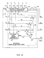
- Fig. 1 shows a block diagram for implementing the invention in an inverter. It consists of a reference modification block (RMB) 1, a PWM block 3, and a semiconductor bridge 5.
- the bridge 5 may be for inversion (Fig. 1), DC to AC, or conversion (Fig. 5), AC to DC.
- the invention compensates voltage deviation in the inverter output.
- the invention compensates voltage deviation in the AC converter input.
- PWM 3 and bridge 5 together comprise a power conversion circuit 7.
- RMB 1 is responsive on lines 2, 4, 6 to three sinusoidal reference voltages U A′ U B′ U C , a triangle voltage U T , and produces three first augmented reference voltages (U A ′and U B ′ and U C ′) on lines 40, 38, 36.
- U A and U B and U C are command reference signals; DC power is obtained from two DC voltage sources U DC /2.
- the three reference voltages (U A and U B and U C ) are spaced 120° apart from one another.
- the first augmented reference voltages (U A ′ and U B ′ and U C ′) are 120° apart.
- RMB 1 consists of three summers 8, 10, and 12, a reference voltage comparator 20, and fourth summer 24 responsive to the magnitude of a triangle peak U TP of the carrier signal U T .
- the magnitude of the carrier signal has a positive peak U TP , and a negative peak -U TP .
- the three reference voltages (U A and U B and U c ) are provided on lines 2, 4, 6 to RMB 1 and to summers 8, 10, 12.
- a reference voltage comparator 20 the magnitudes of each voltage (U A and U B and U C ) are compared and the greatest, U MAX , is produced on a line 22 to a summer 24.
- the reference voltage comparator 20 compares two of the reference voltages and then compares the greater of these two to a third reference voltage to provide U MAX .
- a constant voltage triangle peak value U TP of triangle signal U T is produced in the PWM 3 and provided on line 29 to the summer 24.
- the greatest voltage, U MAX is subtracted from the triangle peak signal U TP on line 29, and the difference U DD provided on lines 34. 32, 30 to summers 8, 10, 12.
- the difference signal U DD is added to each of the reference voltage signals (U A and U B and U C ), thus providing first augmented reference voltage signals (U A ′ and U B ′ and U C ′) which are supplied to a blanking interval voltage deviation compensator 102 over lines 40, 38, and 36.
- a PWM 3 contains three summers 42, 44, 46, three comparators 48, 50, 52, and a triangle signal generator 54.
- Each of the summers 42, 44, and 46 is responsive to second augmented reference voltage signals (U A ⁇ and U B ⁇ and U C ⁇ ) on lines 116, 114, 112 and the triangle signal U T provided by the triangle signal generator 54 onto lines 47, 49, 51.
- the triangle signal generator 54 also provides +U TP on line 29.
- the triangle signal U T has peaks of +U TP and -U TP .
- the summers 42, 44, 46 provide error signals (E A and E B and E C ) to the comparators 48, 50, 52.
- E A , E B or E C is greater than zero (i.e., U X ⁇ is greater than U T )
- the comparators 48, 50, 52 produce switch signals (U SA ⁇ and U SB ⁇ and U SC ⁇ ) on lines 53, 55, 57 and provide them to the bridge 5.
- the bridge 5 includes three legs 56, 58, 60.
- each leg includes two complementary semiconductor switch assemblies.
- the first leg includes a switch S1, a freewheeling diode D1 shunting that switch, and a complementary switching assembly--a NOT gate 62, a switch S1*, and a freewheeling diode D1* shunting that switch.
- the second leg 58 includes a switch S2, a freewheeling diode D2 shunting that switch, and a complementary switching assembly--a switch S2*, a NOT gate 64, and a freewheeling diode D2* shunting that switch.
- the third leg 60 includes a switch S3, a freewheeling diode D3 shunting that switch, and a complementary switching assembly--a switch S3*, a NOT gate 66, and a freewheeling diode D3* shunting that switch.
- An amplitude modulation index m A is defined as a ratio of the peak value of a sinusoidal reference voltage to the peak value U TP .
- m A ⁇ 1 U A and U B and U C , as waveforms 81, 82, 83, are shown in Fig. 2.
- the triangle peak signal U TP is marked on the voltage axis.
- Figs. 2 and 3 are on a common time line and are divided into three sections "A", "B", "C".
- the difference signal (U DD ) produced on line 32 by the summer 24 and equal to the difference between U TP and U MAX is shown by a waveform 80 in Fig. 3.
- U DD causes Uo′o to vary.
- Uo′o is the potential difference between the load midpoint, O′, and the supply midpoint, O.
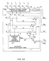
- the microprocessor-based blanking interval voltage deviation compensator 102 is responsive on lines 36, 38, 40 to the first augmented reference voltage U X ′ (where X is A, B, or C) and on lines 103, 105, 107 to reference currents on lines 104, 106, 108, I A ,I B ,I C associated with those reference voltages and to the triangle peak signals ⁇ U TP on line 110. It provides on lines 116, 114, 112 three second augmented reference voltage signals (U A ⁇ and U B ⁇ and U C ⁇ ) for each of the bridge legs 56, 58, 60.
- Fig. 4 shows the logic routine for determining the value of the second augmented reference voltage signals (U A ⁇ and U B ⁇ and U C ⁇ ). For an inverter, voltage deviation in the inverter output is compensated.
- the routine of Fig. 4 provides that if the reference current I X (where X is A, B, or C and I A is associated with U A , I B is associated with U B , etc.) is positive, the blanking interval compensation voltage ⁇ U X is added to the first augmented reference voltage U X ′. On the other hand, if the reference current I X is negative, the same blanking interval compensation voltage ⁇ U X is subtracted from the first augmented reference voltage U X ′.
- An inverter leg 56, 58, 60 is defined as the PWM circuit and the associated bridge leg.
- Fig. 1 there are three inverter legs. Saturation of, for example, the inverter leg 56 occurs when an increase in input reference voltage to the PWM circuit does not yield any greater bridge output voltage. For example, an increase in U A ′ beyond ⁇ U TP will not yield any greater inverter output voltage from that leg 56.
- the routine compensates blanking interval voltage deviation if the inverter leg 56 is not saturated and compensation would not cause the inverter leg to saturate. Because PWM 3 saturates if U X ′ exceeds ⁇ U TP , one can determine if the inverter leg is saturated by determining whether U X ′ is inside or outside ⁇ U TP . One can also determine if compensation is going to cause saturation by determining whether E X is within ⁇ U TP .
- the routine is entered at step 401. If U X ′ is greater than or equal to the triangle peak U TP (a step 404 affirmative), inverter leg is saturated and therefore there is no compensation of a blanking interval voltage, and the input U X ⁇ to PWM 2 is set equal to U TP (a step 406). A similar result is generated if the first augmented reference voltage U X ′ is equal to or less than - U TP (a step 404 negative and step 408 affirmative); U X ⁇ is then set to -U TP (a step 410). If the step 408 is answered negative, the inverter leg 56 is not in saturation.
- the invention does not compensate blanking interval voltage deviation all the time, but only when it is necessary, for example, for a time equivalent to 240° of the reference phase voltage U x .
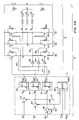
- the invention may be implemented in an inverter circuit as in Fig. 1 or as a converter in Fig. 5.
- the balanced load elements 70 are replaced by inductors and three sinusoidal power sources U D , U E , and U F .
Landscapes
- Engineering & Computer Science (AREA)
- Power Engineering (AREA)
- Inverter Devices (AREA)
- Supply And Distribution Of Alternating Current (AREA)
- Rectifiers (AREA)
Applications Claiming Priority (2)
| Application Number | Priority Date | Filing Date | Title |
|---|---|---|---|
| US07/761,113 US5206802A (en) | 1991-09-17 | 1991-09-17 | Blanking interval voltage deviation compensator for inverters and converters |
| US761113 | 1991-09-17 |
Publications (3)
| Publication Number | Publication Date |
|---|---|
| EP0533403A2 EP0533403A2 (en) | 1993-03-24 |
| EP0533403A3 EP0533403A3 (en) | 1993-08-25 |
| EP0533403B1 true EP0533403B1 (en) | 1995-11-29 |
Family
ID=25061177
Family Applications (1)
| Application Number | Title | Priority Date | Filing Date |
|---|---|---|---|
| EP92308251A Expired - Lifetime EP0533403B1 (en) | 1991-09-17 | 1992-09-10 | Blanking interval voltage deviation compensator for inverters and converters |
Country Status (15)
| Country | Link |
|---|---|
| US (1) | US5206802A (es) |
| EP (1) | EP0533403B1 (es) |
| JP (1) | JPH05227758A (es) |
| KR (1) | KR100268738B1 (es) |
| CN (1) | CN1028943C (es) |
| AU (1) | AU650162B2 (es) |
| BR (1) | BR9203573A (es) |
| CA (1) | CA2077116A1 (es) |
| DE (1) | DE69206371T2 (es) |
| ES (1) | ES2083100T3 (es) |
| FI (1) | FI924083A7 (es) |
| HK (1) | HK63496A (es) |
| MY (1) | MY110333A (es) |
| TW (1) | TW200618B (es) |
| ZA (1) | ZA926459B (es) |
Families Citing this family (13)
| Publication number | Priority date | Publication date | Assignee | Title |
|---|---|---|---|---|
| US5550450A (en) * | 1993-04-28 | 1996-08-27 | Otis Elevator Company | Dead-time effect compensation for pulse-width modulated inverters and converters |
| DE59305367D1 (de) * | 1993-07-26 | 1997-03-13 | Siemens Ag | Verfahren und vorrichtung zur kompensation einer fehlerspannung bei einem pulswechselrichter |
| US5535906A (en) * | 1995-01-30 | 1996-07-16 | Advanced Energy Industries, Inc. | Multi-phase DC plasma processing system |
| US6169334B1 (en) | 1998-10-27 | 2001-01-02 | Capstone Turbine Corporation | Command and control system and method for multiple turbogenerators |
| US6629064B1 (en) | 1999-03-09 | 2003-09-30 | Capstone Turbine Corporation | Apparatus and method for distortion compensation |
| US6603562B1 (en) * | 1999-10-29 | 2003-08-05 | Yokogawa Electric Corporation | Two-dimensional positioning apparatus and method for measuring laser light from the apparatus |
| CN1300922C (zh) * | 2002-07-30 | 2007-02-14 | 台达电子工业股份有限公司 | 同步整流装置 |
| US7397675B2 (en) * | 2006-10-18 | 2008-07-08 | Azure Dynamics, Inc. | Inverter-filter non-linearity blanking time and zero current clamping compensation system and method |
| EP2143196B1 (en) | 2007-03-27 | 2018-08-15 | Danfoss Drives A/S | Method for driving a pulse width modulated controller |
| US7888905B2 (en) * | 2008-01-11 | 2011-02-15 | GM Global Technology Operations LLC | Method and system for controlling a power inverter in electric drives |
| ES2931151T3 (es) * | 2019-06-20 | 2022-12-27 | Toshiba Mitsubishi Elec Ind | Dispositivo de conversión de energía |
| CN115516750A (zh) * | 2020-04-30 | 2022-12-23 | 东芝三菱电机产业系统株式会社 | 电力转换装置及故障解析方法 |
| EP4106178A1 (en) | 2021-06-16 | 2022-12-21 | Goodrich Control Systems | Compensation technique for parallel motor drives |
Family Cites Families (13)
| Publication number | Priority date | Publication date | Assignee | Title |
|---|---|---|---|---|
| JPS58130792A (ja) * | 1982-01-28 | 1983-08-04 | Fanuc Ltd | 同期電動機の駆動装置 |
| JPS5972991A (ja) * | 1982-10-19 | 1984-04-25 | Fanuc Ltd | モ−タの制御装置 |
| US4562386A (en) * | 1984-01-26 | 1985-12-31 | Performance Controls Company | Current sense demodulator |
| US4692854A (en) * | 1986-03-04 | 1987-09-08 | Best Power Technology, Inc | Method and apparatus for modulating inverter pulse width |
| JPH0274192A (ja) * | 1988-09-08 | 1990-03-14 | Toshiba Corp | 電力変換装置 |
| JPH0777516B2 (ja) * | 1989-04-27 | 1995-08-16 | 三菱電機株式会社 | 多相インバータの出力直流分防止装置 |
| GB2238189B (en) * | 1989-05-16 | 1993-12-22 | Mitsubishi Electric Corp | Pulse-width modulation type inverter apparatus |
| JPH078146B2 (ja) * | 1989-05-23 | 1995-01-30 | 春日電機株式会社 | インバータの制御装置 |
| JPH0728537B2 (ja) * | 1989-06-02 | 1995-03-29 | 三菱電機株式会社 | インバータ出力電圧誤差の補正装置 |
| EP0439642B1 (en) * | 1990-01-29 | 1994-08-03 | Kabushiki Kaisha Toshiba | Control apparatus for inverter |
| JP2526700B2 (ja) * | 1990-04-11 | 1996-08-21 | 三菱電機株式会社 | 3相3値レベルインバ―タ |
| US5115386A (en) * | 1990-10-15 | 1992-05-19 | Hitachi, Ltd. | Circuit for controlling an electric power supply apparatus, a method therefor and an uninterruptible power supply |
| US5153821A (en) * | 1991-09-06 | 1992-10-06 | Otis Elevator Company | Pulse-width-modulation method for providing extended linearity, reduced commutation losses and increase in inverter/converter output voltage |
-
1991
- 1991-09-17 US US07/761,113 patent/US5206802A/en not_active Expired - Fee Related
-
1992
- 1992-08-26 TW TW081106742A patent/TW200618B/zh active
- 1992-08-26 ZA ZA926459A patent/ZA926459B/xx unknown
- 1992-08-26 MY MYPI92001536A patent/MY110333A/en unknown
- 1992-08-28 CA CA002077116A patent/CA2077116A1/en not_active Abandoned
- 1992-09-03 AU AU22137/92A patent/AU650162B2/en not_active Ceased
- 1992-09-10 DE DE69206371T patent/DE69206371T2/de not_active Expired - Fee Related
- 1992-09-10 EP EP92308251A patent/EP0533403B1/en not_active Expired - Lifetime
- 1992-09-10 ES ES92308251T patent/ES2083100T3/es not_active Expired - Lifetime
- 1992-09-11 FI FI924083A patent/FI924083A7/fi not_active Application Discontinuation
- 1992-09-14 JP JP4244404A patent/JPH05227758A/ja active Pending
- 1992-09-14 BR BR929203573A patent/BR9203573A/pt not_active Application Discontinuation
- 1992-09-16 KR KR1019920016832A patent/KR100268738B1/ko not_active Expired - Fee Related
- 1992-09-17 CN CN92110724A patent/CN1028943C/zh not_active Expired - Fee Related
-
1996
- 1996-04-11 HK HK63496A patent/HK63496A/en not_active IP Right Cessation
Also Published As
| Publication number | Publication date |
|---|---|
| ZA926459B (en) | 1993-03-04 |
| AU2213792A (en) | 1993-03-25 |
| BR9203573A (pt) | 1993-04-13 |
| KR100268738B1 (en) | 2000-10-16 |
| ES2083100T3 (es) | 1996-04-01 |
| KR930007051A (ko) | 1993-04-22 |
| TW200618B (es) | 1993-02-21 |
| FI924083A0 (fi) | 1992-09-11 |
| US5206802A (en) | 1993-04-27 |
| CA2077116A1 (en) | 1993-03-18 |
| CN1070776A (zh) | 1993-04-07 |
| DE69206371T2 (de) | 1996-05-09 |
| JPH05227758A (ja) | 1993-09-03 |
| MY110333A (en) | 1998-04-30 |
| DE69206371D1 (de) | 1996-01-11 |
| AU650162B2 (en) | 1994-06-09 |
| HK63496A (en) | 1996-04-19 |
| CN1028943C (zh) | 1995-06-14 |
| EP0533403A3 (en) | 1993-08-25 |
| EP0533403A2 (en) | 1993-03-24 |
| FI924083A7 (fi) | 1993-03-18 |
Similar Documents
| Publication | Publication Date | Title |
|---|---|---|
| US5153821A (en) | Pulse-width-modulation method for providing extended linearity, reduced commutation losses and increase in inverter/converter output voltage | |
| EP0533403B1 (en) | Blanking interval voltage deviation compensator for inverters and converters | |
| US5550450A (en) | Dead-time effect compensation for pulse-width modulated inverters and converters | |
| Holtz | Pulsewidth modulation-a survey | |
| JP2577738B2 (ja) | Pwmインバ−タ装置 | |
| Loh et al. | Modular hysteresis current control of hybrid multilevel inverters | |
| Chen et al. | Multiple PR current regulator based dead-time effects compensation for grid-forming single-phase inverter | |
| KR920010235B1 (ko) | 펄스폭 변조승압 변환기의 제어장치 | |
| JP3296425B2 (ja) | 電力変換装置 | |
| JP2527911B2 (ja) | Pwmコンバ―タ | |
| JP4755504B2 (ja) | 電力変換装置 | |
| Fu et al. | Super-twisting sliding mode control for neutral point voltage of three-phase four-wire inverter based on SiC/Si hybrid switch | |
| Ljusev et al. | Safe-commutation principle for direct single-phase ac-ac converters for use in audio power amplification | |
| JP3286046B2 (ja) | 電力変換装置の制御方法 | |
| Jung et al. | A PI-type dead-time compensation method for vector-controlled GTO inverters | |
| JPH077944A (ja) | 電力変換装置の制御方法 | |
| JP4277360B2 (ja) | 3レベルインバータの制御装置 | |
| Bonthagorla et al. | Performance analysis of closed loop controlled single-phase unipolar inverter with fixed switching frequency sliding mode control | |
| JP3133537B2 (ja) | 交流電動機のpwm制御装置 | |
| JPH05146161A (ja) | Pwm変換装置 | |
| JP2006166664A (ja) | 電圧形インバータの制御方法 | |
| JPH05336754A (ja) | 並列多重インバータ装置 | |
| Ben-Brahim et al. | A new PWM control for GTO minimum on-pulse compensation | |
| WO2025059765A1 (en) | Pulse distortion compensation for pulse-width-modulation based converters | |
| JPH05219754A (ja) | 電力変換装置 |
Legal Events
| Date | Code | Title | Description |
|---|---|---|---|
| PUAI | Public reference made under article 153(3) epc to a published international application that has entered the european phase |
Free format text: ORIGINAL CODE: 0009012 |
|
| AK | Designated contracting states |
Kind code of ref document: A2 Designated state(s): DE ES FR GB IT |
|
| PUAL | Search report despatched |
Free format text: ORIGINAL CODE: 0009013 |
|
| AK | Designated contracting states |
Kind code of ref document: A3 Designated state(s): DE ES FR GB IT |
|
| 17P | Request for examination filed |
Effective date: 19940203 |
|
| 17Q | First examination report despatched |
Effective date: 19941207 |
|
| GRAA | (expected) grant |
Free format text: ORIGINAL CODE: 0009210 |
|
| ITF | It: translation for a ep patent filed | ||
| AK | Designated contracting states |
Kind code of ref document: B1 Designated state(s): DE ES FR GB IT |
|
| REF | Corresponds to: |
Ref document number: 69206371 Country of ref document: DE Date of ref document: 19960111 |
|
| ET | Fr: translation filed | ||
| REG | Reference to a national code |
Ref country code: ES Ref legal event code: FG2A Ref document number: 2083100 Country of ref document: ES Kind code of ref document: T3 |
|
| PLBE | No opposition filed within time limit |
Free format text: ORIGINAL CODE: 0009261 |
|
| 26N | No opposition filed | ||
| PGFP | Annual fee paid to national office [announced via postgrant information from national office to epo] |
Ref country code: FR Payment date: 20000807 Year of fee payment: 9 |
|
| PGFP | Annual fee paid to national office [announced via postgrant information from national office to epo] |
Ref country code: GB Payment date: 20000811 Year of fee payment: 9 |
|
| PGFP | Annual fee paid to national office [announced via postgrant information from national office to epo] |
Ref country code: DE Payment date: 20000823 Year of fee payment: 9 |
|
| PGFP | Annual fee paid to national office [announced via postgrant information from national office to epo] |
Ref country code: ES Payment date: 20000911 Year of fee payment: 9 |
|
| PG25 | Lapsed in a contracting state [announced via postgrant information from national office to epo] |
Ref country code: GB Free format text: LAPSE BECAUSE OF NON-PAYMENT OF DUE FEES Effective date: 20010910 |
|
| PG25 | Lapsed in a contracting state [announced via postgrant information from national office to epo] |
Ref country code: ES Free format text: LAPSE BECAUSE OF NON-PAYMENT OF DUE FEES Effective date: 20010911 |
|
| GBPC | Gb: european patent ceased through non-payment of renewal fee |
Effective date: 20010910 |
|
| PG25 | Lapsed in a contracting state [announced via postgrant information from national office to epo] |
Ref country code: DE Free format text: LAPSE BECAUSE OF NON-PAYMENT OF DUE FEES Effective date: 20020501 |
|
| PG25 | Lapsed in a contracting state [announced via postgrant information from national office to epo] |
Ref country code: FR Free format text: LAPSE BECAUSE OF NON-PAYMENT OF DUE FEES Effective date: 20020531 |
|
| REG | Reference to a national code |
Ref country code: FR Ref legal event code: ST |
|
| REG | Reference to a national code |
Ref country code: ES Ref legal event code: FD2A Effective date: 20021011 |
|
| PG25 | Lapsed in a contracting state [announced via postgrant information from national office to epo] |
Ref country code: IT Free format text: LAPSE BECAUSE OF NON-PAYMENT OF DUE FEES;WARNING: LAPSES OF ITALIAN PATENTS WITH EFFECTIVE DATE BEFORE 2007 MAY HAVE OCCURRED AT ANY TIME BEFORE 2007. THE CORRECT EFFECTIVE DATE MAY BE DIFFERENT FROM THE ONE RECORDED. Effective date: 20050910 |