EP0525533B1 - Supraleitende Detektionsspulen - Google Patents
Supraleitende Detektionsspulen Download PDFInfo
- Publication number
- EP0525533B1 EP0525533B1 EP92112177A EP92112177A EP0525533B1 EP 0525533 B1 EP0525533 B1 EP 0525533B1 EP 92112177 A EP92112177 A EP 92112177A EP 92112177 A EP92112177 A EP 92112177A EP 0525533 B1 EP0525533 B1 EP 0525533B1
- Authority
- EP
- European Patent Office
- Prior art keywords
- superconducting
- detection coils
- wiring pattern
- wiring
- flexible printed
- Prior art date
- Legal status (The legal status is an assumption and is not a legal conclusion. Google has not performed a legal analysis and makes no representation as to the accuracy of the status listed.)
- Expired - Lifetime
Links
Images


Classifications
-
- G—PHYSICS
- G01—MEASURING; TESTING
- G01R—MEASURING ELECTRIC VARIABLES; MEASURING MAGNETIC VARIABLES
- G01R33/00—Arrangements or instruments for measuring magnetic variables
- G01R33/02—Measuring direction or magnitude of magnetic fields or magnetic flux
- G01R33/035—Measuring direction or magnitude of magnetic fields or magnetic flux using superconductive devices
- G01R33/0354—SQUIDS
- G01R33/0358—SQUIDS coupling the flux to the SQUID
-
- G—PHYSICS
- G01—MEASURING; TESTING
- G01R—MEASURING ELECTRIC VARIABLES; MEASURING MAGNETIC VARIABLES
- G01R33/00—Arrangements or instruments for measuring magnetic variables
- G01R33/02—Measuring direction or magnitude of magnetic fields or magnetic flux
- G01R33/022—Measuring gradient
-
- Y—GENERAL TAGGING OF NEW TECHNOLOGICAL DEVELOPMENTS; GENERAL TAGGING OF CROSS-SECTIONAL TECHNOLOGIES SPANNING OVER SEVERAL SECTIONS OF THE IPC; TECHNICAL SUBJECTS COVERED BY FORMER USPC CROSS-REFERENCE ART COLLECTIONS [XRACs] AND DIGESTS
- Y10—TECHNICAL SUBJECTS COVERED BY FORMER USPC
- Y10S—TECHNICAL SUBJECTS COVERED BY FORMER USPC CROSS-REFERENCE ART COLLECTIONS [XRACs] AND DIGESTS
- Y10S505/00—Superconductor technology: apparatus, material, process
- Y10S505/825—Apparatus per se, device per se, or process of making or operating same
- Y10S505/842—Measuring and testing
- Y10S505/843—Electrical
- Y10S505/845—Magnetometer
- Y10S505/846—Magnetometer using superconductive quantum interference device, i.e. squid
-
- Y—GENERAL TAGGING OF NEW TECHNOLOGICAL DEVELOPMENTS; GENERAL TAGGING OF CROSS-SECTIONAL TECHNOLOGIES SPANNING OVER SEVERAL SECTIONS OF THE IPC; TECHNICAL SUBJECTS COVERED BY FORMER USPC CROSS-REFERENCE ART COLLECTIONS [XRACs] AND DIGESTS
- Y10—TECHNICAL SUBJECTS COVERED BY FORMER USPC
- Y10S—TECHNICAL SUBJECTS COVERED BY FORMER USPC CROSS-REFERENCE ART COLLECTIONS [XRACs] AND DIGESTS
- Y10S505/00—Superconductor technology: apparatus, material, process
- Y10S505/825—Apparatus per se, device per se, or process of making or operating same
- Y10S505/88—Inductor
-
- Y—GENERAL TAGGING OF NEW TECHNOLOGICAL DEVELOPMENTS; GENERAL TAGGING OF CROSS-SECTIONAL TECHNOLOGIES SPANNING OVER SEVERAL SECTIONS OF THE IPC; TECHNICAL SUBJECTS COVERED BY FORMER USPC CROSS-REFERENCE ART COLLECTIONS [XRACs] AND DIGESTS
- Y10—TECHNICAL SUBJECTS COVERED BY FORMER USPC
- Y10T—TECHNICAL SUBJECTS COVERED BY FORMER US CLASSIFICATION
- Y10T29/00—Metal working
- Y10T29/49—Method of mechanical manufacture
- Y10T29/49002—Electrical device making
- Y10T29/4902—Electromagnet, transformer or inductor
Definitions
- the present invention relates to the structure of detection coils used in a magnetic sensor employing superconducting quantum interference devices (SQUIDs) which are applied to high-sensitivity magnetic sensors.
- SQUIDs superconducting quantum interference devices
- Fig. 10 shows conventional first-derivative detection coils of the bobbin type. Shown are a bobbin 11, a superconducting coil wire 12, electrodes 13, and a damping resistor 14.
- the superconducting coil wire 12 is so arranged in a groove formed in the bobbin 11 that upper and lower coils are wound in opposite senses.
- the superconducting coil wire 12 is connected with the electrodes 13 which are connected with the damping resistor 14.
- Fig. 11 shows the structure of conventional second-derivative detection coils of the bobbin type.
- Upper and lower coils are wound in the same sense.
- An intermediate coil is wound in the opposite sense with turns twice as many as the number of turns of the upper and lower coils.
- the wires of the first-derivative and second-derivative detection coils of the bobbin type are strands except for the coils to prevent magnetic flux from intersecting the wires.
- the first-derivative detection coil of the bobbin type detects the difference between the magnetic field signal detected by the upper coil and the magnetic field signal detected by the lower coil, i.e., the magnetic gradient is detected.
- the second-derivative detection coil of the bobbin type detects the difference between the magnetic field gradient detected by the upper and intermediate coils and the magnetic field gradient detected by the intermediate lower coils. Therefore, the accuracy of the areas of the coils, the shape accuracy, the accuracy of the positional relation between them, the accuracy of the degree of the parallelism between them, and other factors affect the magnetic gradient sensitivity.
- the groove in the bobbin which accommodates the superconducting coil wire is required to be machined with high accuracy.
- a triangular gap is formed at the boundary between each circular coil portion and the strand. This makes it difficult to improve the accuracy of the areas of the coils, the shape accuracy, the accuracy of the positional relation between them, and the accuracy of the degree of the parallelism between them. As a result, the magnetic field gradient sensitivity and the reproducibility of the characteristics are deteriorated.
- the coils are difficult to manufacture, because skilfulness is needed for the manufacture.
- EP-A-0185186 discloses superconducting detection coils according to the preamble of claim 1.
- the superconductor gradiometer of EP-A-0 185 186 requires the gradiometer coils be placed in spaced position with connecting lines therebetween on a large planar body.
- the planar body is then formed into a three-dimensional gradiometer structure, which is then applied to a support body.
- the gradiometer coils 4 and 5 are preformed onto the planar flexible member before the planar flexible member is bent into a three-dimensional shape. Then, a relatively complex bending operation is required to dispose the coils 4 and 5 at appropriate relative positions.
- a resistor may or may not be formed on the film.
- the superconducting wiring pattern has a substantially U-shaped wiring portion formed in a portion thereof.
- the U-shaped wiring portion forms cylindrical wiring patterns.
- the detection coil wiring pattern and the pattern of the resistor can be fabricated by ordinary printed wiring film conductive pattern fabrication techniques.
- the flexible film is merely bent into a cylinder.
- the superconducting detection coils can be easily fabricated. Consequently, the accuracy of the areas of the upper and lower coils, the shape accuracy, the accuracy of the positional relation between them, and the accuracy of the degree of the parallelism between them can be improved. Furthermore, the absolute accuracy of the resistance value and the absolute accuracy between the plural superconducting detection coils can be improved.
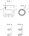
- Fig. 1 shows the pattern of wiring on a flexible printed wiring film for a first-derivative detection coil of the bobbin type, thus showing example 1 of the invention. Shown components are the flexible printed wiring film 1, a superconducting wiring pattern 2, electrodes 3, a resistive interconnect 4.
- the flexible printed wiring film 1 consists of polyimide.
- the superconducting wiring pattern 2 and the electrodes 3 are fabricated by plating of lead-zinc (Pb-Sn), sputtering of niobium (Nb), or deposition of lead-indium (Pb-In).
- Other wiring of a superconducting thin or thick film may also be used as the pattern 2 or as the electrodes 3.
- a buffer layer for the film of the Pb-Sn plating is used and consists of a resistive material such as copper (Cu) or palladium (Pd). Other high-resistivity materials can also be employed.
- the resistive interconnect 4 is made of a resistive material similar to the material used for the buffer layer for the Pb-Sn plating film.
- the flexible printed wiring film is rounded such that the portion indicated by A in Fig. 1 and the portion indicated by B overlap each other.
- first-derivative detection coils of one turn of the structure shown in Fig. 3 can be fabricated.
- the arrows of Fig. 3 indicate the directions of winding of the coils.
- first-derivative detection coils of two turns of the structure shown in Fig. 4 can be fabricated by rounding the flexible printed wiring film two turns such that the portions A, C, and B of Fig. 1 overlap each other.
- the arrows of Fig. 4 indicate the directions of winding of the coils.
- Fig. 2 is a cross-sectional view showing the structure of the first-derivative bobbin-type detection coils, showing example 1 of the present invention. Shown are a bobbin 6 and a cover 7.
- the flexible printed wiring film 1 on which the superconducting wiring pattern shown in Fig. 1 is formed is wound around the bobbin 6.
- the cylindrical cover 7 is disposed.
- the bobbin 6 which may be a solid or hollow cylinder is made of FRP, glass, Teflon, or other material.
- the cover 7 that is cylindrical in shape is made of FRP, glass, Teflon, or other material.
- Fig. 5 shows the wiring pattern on a flexible printed wiring film for second-derivative bobbin-type detection coils, showing example 2 of the present invention.
- the flexible printed wiring film 1, the superconducting wiring pattern 2, the buffer layer for the Pb-Sn plating film, the electrodes 3, and the resistive interconnect 4 are made of the same materials as those of the counterparts of example 1. Electrical conduction is prevented at the intersection of wires indicated by A in Fig. 5.
- an insulating material such as urethane.
- Second-derivative detection coils having one upper turn, two intermediate turns, and one lower turn, respectively, as shown in Fig. 6 can be fabricated by winding the device two turns such that the portions A, B and C of Fig. 5 overlap each other.
- the arrows of Fig. 6 indicate the directions of winding of the coils.
- second-derivative detection coils having two upper turns, four intermediate turns, and two lower turns, respectively, as shown in Fig. 5 can be fabricated by winding the device four turns such that the portions A, B, and C of Fig. 5 overlap each other.
- Fig. 7 shows the wiring pattern on a flexible printed wiring film for first-derivative bobbin-type detection coils, showing example 3 of the present invention.
- the wire portions B-D and E-F are equal in length.
- the flexible printed wiring film 1, the superconducting wiring pattern 2, the buffer layer for the Pb-Sn plating film, the electrodes 3, and the resistive interconnect 4 are made of the same materials as those of the counterparts of example 1.
- First-derivative detection coils of one turn and two turns, respectively, can be fabricated by rounding the flexible film in one turn and two turns, respectively, such that D is placed on the position C located midway between A and B of Fig. 7.
- the area of the upper coil can be made exactly coincident with the area of the lower coil of the finished detection coils by laying the wire portion A-E of the superconducting wiring pattern 2 of Fig. 7 at an angle such that the wire portions B-D and E-F agree in length.
- Noise produced laterally of the detection coils can be reduced by rounding the flexible film in such a way that the center of the wire portion D-F is placed on the center of the wire portion A-E of Fig. 7.
- Fig. 8 shows the wiring pattern on a flexible printed wiring film for first-derivative bobbin-type detection coils, showing example 4 of the present invention.
- the flexible printed wiring film 1, the superconducting wiring pattern 2, the buffer layer for the Pb-Sn plating film, the electrodes 3, and the resistive interconnect 4 are made of the same materials as those of the counterparts of example 1.
- the superconducting wiring pattern 2 is formed on both surfaces of the flexible printed wiring film 1 or on different layers. Electrical conduction between the portions formed on both surfaces of the flexible printed wiring film 1 or on the different layers is permitted by superconductors passed through contact holes 5 formed in the buffer layer and in the flexible printed wiring film 1.
- First-derivative detection coils of one turn and two turns, respectively, are fabricated by rounding the flexible film one turn and two turns, respectively, such that portion B is placed on portion A of Fig. 8.
- Fig. 9 shows the wiring pattern on a flexible printed wiring film of first-derivative bobbin-type detection coils, showing example 5 of the present invention.
- the flexible wiring printed film 1, the superconducting wiring pattern 2, the buffer layer for the Pb-Sn plating film, the electrodes 3, and the resistive interconnect 4 are made of the same materials as those of the counterparts of example 1.
- the superconducting wiring pattern 2 is formed on both surfaces of the flexible printed film 1 or on different layers in the same way as in example 4.
- the wires of the superconducting wiring pattern extend from the electrodes 3 between portions A and B to the front and rear surfaces or to different layers of the flexible printed wiring film 1 in a staggered relation to each other to remove lateral noise caused by external magnetic disturbance.
- First-derivative detection coils of one turn and two turns, respectively, are fabricated by rounding the flexible film one turn and two turns, respectively, such that portion D is placed on position C located midway between portions A and B of Fig. 9.
- first- or higher order-derivative superconducting detection coils of any desired turns can be fabricated by shaping a flexible printed wiring film having a coil wiring pattern into a cylinder.
- the accuracy of the circular areas of the coils, the shape accuracy, the accuracy of the positional relation between them, and the accuracy of the degree of the parallelism between them can be extremely improved.
- the absolute accuracy of the damping resistor and the relative accuracy between plural superconducting detection coils can be improved.
- the magnetic filed gradient sensitivity and the reproducibility of the magnetic characteristics can be enhanced.
- superconducting detection coils can be easily fabricated by shaping a flexible printed wiring film having superconducting film wiring and a resistive interconnect into a cylinder.
- the accuracy of the circular areas of the upper and lower coils, the shape accuracy, the accuracy of the positional relation between them, and the accuracy of the degree of the parallelism between them can be extremely improved.
- the absolute accuracy of the damping resistor and the relative accuracy between plural superconducting detection coils can be improved.
- the magnetic field gradient sensitivity and the reproducibility of the magnetic characteristics can be enhanced.
Landscapes
- Physics & Mathematics (AREA)
- Condensed Matter Physics & Semiconductors (AREA)
- General Physics & Mathematics (AREA)
- Measuring Magnetic Variables (AREA)
Claims (8)
- Supraleitende Detektionsspulen für einen Supraleiter-Quanteninterferometer, wobei die Spulen eine flexible Folie (1) für gedruckte Schaltungen aufweisen, auf der ein supraleitendes Schaltungsmuster (2) ausgebildet ist und die in Zylinderform ausgebildet ist, dadurch gekennzeichnet, daß das supraleitende Schaltungsmuster (2) im wesentlichen U-förmige Schaltungsteile aufweist, die mindestens ein Paar oberer und unterer zylindrischer Schaltungsmuster bilden, wenn die flexible Folie (1) für gedruckte Schaltungen (1) zu einem Zylinder geformt wird, wobei der im wesentlichen U-förmige Schaltungsteil zwei Schenkelteile aufweist, die durch einen Basisteil querverbunden sind, sich die Schenkelteile gegenseitig überlagern, um die zylindrischen Schaltungsmuster auszubilden, wenn die flexible Folie (1) für gedruckte Schaltungen zu einem Zylinder geformt wird; und Elektroden (3) aufweist, die jeweils mit dem entsprechenden Schenkelteil des im wesentlichen U-förmig ausgebildeten Schaltungsteils zwecks Ankoppelns der zylindricher Schaltungsmuster an wenigstens einen supraleitenden Quanteninterferometer verbunden sind.
- Supraleitende Detektionsspulen gemäß Anspruch 1, die ferner enthalten einen Widerstand (4) der elektrisch parallel an das supraleitende Schaltungsmuster (2) angeschlossen ist.
- Supraleitende Detektionsspulen gemäß Anspruch 1, bei denen das supraleitende Schaltungsmuster (2) wenigstens zwei im wesentlichen U-förmige Schaltungsteile aufweist zwecks Ausbildens von mindestens drei zylindrischen Schaltungsmustern, wenn die flexible Folie (1) für gedruckte Schaltung zu einem Zylinder geformt wird.
- Supraleitende Detektionsspulen gemäß Anspruch 1, bei denen die zwei Schenkelteile gleich lang sind, so daß ein Bereich eines zylindrischen Schaltungsmusters, der von einem Schenkelteil gebildet wird, genau so ist wie ein Bereich eines zylindrischen Schaltungsmusters, der vom anderen Schenkelteil gebildet wird, wenn die flexible Folie (1) für eine gedruckte Schaltung zu einem Zylinder geformt wird.
- Supraleitende Detektionsspulen gemäß Anspruch 1, bei denen das supraleitende Schaltungsmuster (2) eine vordere Oberfläche und eine hintere Oberfläche aufweist und durchgehende Löcher (5) zwischen der hinteren Oberfläche und der vorderen Oberfläche ausgebildet sind; und das supraleitende Schaltungsmuster sowohl auf der vorderen Oberfläche als auch auf der hinteren Oberfläche ausgebildet ist und durch die durchgehenden Löcher (5) elektrisch verbunden sind.
- Supraleitende Detektionsspulen gemäß Anspruch 5, bei denen die zwei Schenkelteile auf einer, der vorderen oder der hinteren Oberfläche, ausgebildet sind, wobei ein Schenkelteil mit einem Teil des auf der anderen, der vorderen Oberfläche bzw. der hinteren Oberfläche ausgebildeten Schaltungsmusters durch die durchgehenden Löcher verbunden ist.
- Supraleitende Detektionsspulen gemäß Anspruch 5, bei denen die zwei Schenkelteile auf einer, der vorderen oder der hinteren, Oberfläche ausgebildet sind; und das supraleitende Schaltungsmuster (2) einen ersten Anschlußteil beinhaltet, der auf beiden, der vorderen und der hinteren, Oberflächen ausgebildet ist und durch die durchgehenden Löcher (5) verbunden ist, und ein zweiter Verbindungsteil auf beiden, der vorderen und der hinteren, Oberflächen ausgebildet ist und durch die durchgehenden Löcher (5) verbunden ist, wobei sich der erste und der zweite Verbindungsteil überlappen und die flexible Folie (1) für gedruckte Schaltungen zwischen ihnen liegt, und der erste Verbindungsteil zwischen einem, der Elektrode (3) und dem Schenkelteil, und der zweite Verbindungsteil zwischen der anderen Elektrode (3) und dem anderen Schenkelteil verbunden ist, so daß die überlappenden Verbindungsteile, der erste und der zweite Verbindungssteil, von externen magnetischen Störungen verursachtes Rauschen effektiv ausschaltet.
- Supraleitende Detektionsspulen gemäß Anspruch 1, bei denen die zwei Schenkelteile parallel sind und der Basisteil senkrecht auf den zwei Schenkelteilen steht.
Applications Claiming Priority (4)
| Application Number | Priority Date | Filing Date | Title |
|---|---|---|---|
| JP186495/91 | 1991-07-25 | ||
| JP18649591 | 1991-07-25 | ||
| JP4157764A JP2909790B2 (ja) | 1991-07-25 | 1992-06-17 | 超伝導検出コイル |
| JP157764/92 | 1992-06-17 |
Publications (3)
| Publication Number | Publication Date |
|---|---|
| EP0525533A2 EP0525533A2 (de) | 1993-02-03 |
| EP0525533A3 EP0525533A3 (en) | 1993-09-29 |
| EP0525533B1 true EP0525533B1 (de) | 1997-09-24 |
Family
ID=26485098
Family Applications (1)
| Application Number | Title | Priority Date | Filing Date |
|---|---|---|---|
| EP92112177A Expired - Lifetime EP0525533B1 (de) | 1991-07-25 | 1992-07-16 | Supraleitende Detektionsspulen |
Country Status (3)
| Country | Link |
|---|---|
| US (1) | US5329229A (de) |
| EP (1) | EP0525533B1 (de) |
| DE (1) | DE69222378T2 (de) |
Families Citing this family (6)
| Publication number | Priority date | Publication date | Assignee | Title |
|---|---|---|---|---|
| DE19505812C2 (de) * | 1995-02-09 | 1997-02-06 | Siemens Ag | Stromerfassungsspule für einen Stromwandler |
| US5940116A (en) * | 1996-02-13 | 1999-08-17 | Samsung Electronics Co., Ltd. | Device for connecting an option tray of a laser beam printer simultaneously with the placement thereof |
| EP2145197A4 (de) * | 2007-05-04 | 2011-07-27 | California Inst Of Techn | Geometrien für supraleitende erfassungsspulen für systeme auf squid-basis |
| WO2008137485A2 (en) * | 2007-05-04 | 2008-11-13 | California Institute Of Technology | Low field squid mri devices, components and methods |
| US8132406B2 (en) * | 2009-03-02 | 2012-03-13 | Thompson Randall Jr | Tide activated device to operate a turbine generator |
| EP3267213A1 (de) * | 2016-07-08 | 2018-01-10 | Biomagnetik Park GmbH | Sensor zur messung magnetischer felder |
Family Cites Families (5)
| Publication number | Priority date | Publication date | Assignee | Title |
|---|---|---|---|---|
| GB1268023A (en) * | 1970-02-20 | 1972-03-22 | Marconi Co Ltd | Improvements in or relating to printed circuit magnetic field coils |
| US4320341A (en) * | 1980-01-17 | 1982-03-16 | Sperry Corporation | Method and apparatus for balancing the magnetic field detecting loops of a cryogenic gradiometer using trimming coils and superconducting disks |
| NZ207264A (en) * | 1984-02-23 | 1988-10-28 | New Zealand Dev Finance | Flexible printed circuit coil |
| EP0185186B1 (de) * | 1984-11-19 | 1989-02-01 | Siemens Aktiengesellschaft | Verfahren zur Herstellung eines dreidimensionalen Gradiometers für eine Vorrichtung zur ein- oder mehrkanaligen Messung schwacher Magnetfelder |
| DE3906981A1 (de) * | 1989-03-04 | 1990-09-06 | Philips Patentverwaltung | Supraleitendes gradiometer zur messung schwacher magnetfelder und ein verfahren zu seiner herstellung |
-
1992
- 1992-07-15 US US07/914,894 patent/US5329229A/en not_active Expired - Fee Related
- 1992-07-16 DE DE69222378T patent/DE69222378T2/de not_active Expired - Fee Related
- 1992-07-16 EP EP92112177A patent/EP0525533B1/de not_active Expired - Lifetime
Also Published As
| Publication number | Publication date |
|---|---|
| DE69222378T2 (de) | 1998-01-15 |
| US5329229A (en) | 1994-07-12 |
| DE69222378D1 (de) | 1997-10-30 |
| EP0525533A2 (de) | 1993-02-03 |
| EP0525533A3 (en) | 1993-09-29 |
Similar Documents
| Publication | Publication Date | Title |
|---|---|---|
| US5053834A (en) | High symmetry dc SQUID system | |
| JPH04265875A (ja) | 平面型グラジオメータ | |
| US4982157A (en) | Superconducting gradiometer loop system of a multichannel measuring device | |
| JP3093135B2 (ja) | 平面ソレノイド及び平面ソレノイドを用いたsquid磁力計 | |
| JPH05332703A (ja) | 長尺型磁気センサ | |
| US5568051A (en) | Magnetic resonance imaging apparatus having superimposed gradient coil | |
| EP0525533B1 (de) | Supraleitende Detektionsspulen | |
| US6344742B1 (en) | Magnetic field sensor having a flux guide to increase the effective capture area | |
| CA1138957A (en) | Magnetoresistive position transducer | |
| US4733180A (en) | Apparatus for measuring weak magnetic fields having superconducting connections between a squid array and a gradiometer array | |
| CA2057454C (en) | Pickup coil for measurement of magnetic fields | |
| JPH11507436A (ja) | 複合超電導量子干渉素子および回路 | |
| JPH0563922B2 (de) | ||
| JPH08313609A (ja) | 径方向微分型squid磁束計 | |
| EP1092984A2 (de) | Squid | |
| US5901453A (en) | Gradiometer | |
| JP4415159B2 (ja) | 磁気センサに用いるピックアップコイル | |
| JP2909790B2 (ja) | 超伝導検出コイル | |
| US20030085790A1 (en) | Inductive micro-sensor formed flat on an integrated circuit | |
| US4743852A (en) | Coil for NMR probe | |
| JP3018540B2 (ja) | 3軸型グラジオメータ | |
| EP0753757B1 (de) | Planarer magnetischer Sensor mit einem SQUID aus supraleitender Dünnschicht | |
| JP2592965Y2 (ja) | 超伝導検出コイル | |
| EP0408303B1 (de) | Aufnehmerspulenanordnung für Mehrkanalsquidmagnetometer | |
| JPH06109820A (ja) | 3次元検出コイル |
Legal Events
| Date | Code | Title | Description |
|---|---|---|---|
| PUAI | Public reference made under article 153(3) epc to a published international application that has entered the european phase |
Free format text: ORIGINAL CODE: 0009012 |
|
| AK | Designated contracting states |
Kind code of ref document: A2 Designated state(s): DE FR GB NL |
|
| PUAL | Search report despatched |
Free format text: ORIGINAL CODE: 0009013 |
|
| AK | Designated contracting states |
Kind code of ref document: A3 Designated state(s): DE FR GB NL |
|
| 17P | Request for examination filed |
Effective date: 19931126 |
|
| 17Q | First examination report despatched |
Effective date: 19960117 |
|
| GRAG | Despatch of communication of intention to grant |
Free format text: ORIGINAL CODE: EPIDOS AGRA |
|
| GRAH | Despatch of communication of intention to grant a patent |
Free format text: ORIGINAL CODE: EPIDOS IGRA |
|
| GRAH | Despatch of communication of intention to grant a patent |
Free format text: ORIGINAL CODE: EPIDOS IGRA |
|
| GRAA | (expected) grant |
Free format text: ORIGINAL CODE: 0009210 |
|
| AK | Designated contracting states |
Kind code of ref document: B1 Designated state(s): DE FR GB NL |
|
| ET | Fr: translation filed | ||
| REF | Corresponds to: |
Ref document number: 69222378 Country of ref document: DE Date of ref document: 19971030 |
|
| PLBE | No opposition filed within time limit |
Free format text: ORIGINAL CODE: 0009261 |
|
| STAA | Information on the status of an ep patent application or granted ep patent |
Free format text: STATUS: NO OPPOSITION FILED WITHIN TIME LIMIT |
|
| 26N | No opposition filed | ||
| REG | Reference to a national code |
Ref country code: GB Ref legal event code: IF02 |
|
| REG | Reference to a national code |
Ref country code: GB Ref legal event code: 732E |
|
| NLS | Nl: assignments of ep-patents |
Owner name: SII NANOTECHNOLOGY INC. |
|
| PGFP | Annual fee paid to national office [announced via postgrant information from national office to epo] |
Ref country code: NL Payment date: 20060703 Year of fee payment: 15 |
|
| PGFP | Annual fee paid to national office [announced via postgrant information from national office to epo] |
Ref country code: GB Payment date: 20060712 Year of fee payment: 15 |
|
| PGFP | Annual fee paid to national office [announced via postgrant information from national office to epo] |
Ref country code: DE Payment date: 20060713 Year of fee payment: 15 |
|
| PGFP | Annual fee paid to national office [announced via postgrant information from national office to epo] |
Ref country code: FR Payment date: 20060719 Year of fee payment: 15 |
|
| GBPC | Gb: european patent ceased through non-payment of renewal fee |
Effective date: 20070716 |
|
| NLV4 | Nl: lapsed or anulled due to non-payment of the annual fee |
Effective date: 20080201 |
|
| PG25 | Lapsed in a contracting state [announced via postgrant information from national office to epo] |
Ref country code: NL Free format text: LAPSE BECAUSE OF NON-PAYMENT OF DUE FEES Effective date: 20080201 Ref country code: DE Free format text: LAPSE BECAUSE OF NON-PAYMENT OF DUE FEES Effective date: 20080201 |
|
| PG25 | Lapsed in a contracting state [announced via postgrant information from national office to epo] |
Ref country code: GB Free format text: LAPSE BECAUSE OF NON-PAYMENT OF DUE FEES Effective date: 20070716 |
|
| REG | Reference to a national code |
Ref country code: FR Ref legal event code: ST Effective date: 20080331 |
|
| PG25 | Lapsed in a contracting state [announced via postgrant information from national office to epo] |
Ref country code: FR Free format text: LAPSE BECAUSE OF NON-PAYMENT OF DUE FEES Effective date: 20070731 |