EP0521676A1 - Dünnschicht-Kapazität in einer integrierten Schaltung eines Halbleiterbauelementes und Verfahren zu ihrer Herstellung - Google Patents
Dünnschicht-Kapazität in einer integrierten Schaltung eines Halbleiterbauelementes und Verfahren zu ihrer Herstellung Download PDFInfo
- Publication number
- EP0521676A1 EP0521676A1 EP92305954A EP92305954A EP0521676A1 EP 0521676 A1 EP0521676 A1 EP 0521676A1 EP 92305954 A EP92305954 A EP 92305954A EP 92305954 A EP92305954 A EP 92305954A EP 0521676 A1 EP0521676 A1 EP 0521676A1
- Authority
- EP
- European Patent Office
- Prior art keywords
- film
- dielectric film
- interlayer insulating
- lower electrode
- forming
- Prior art date
- Legal status (The legal status is an assumption and is not a legal conclusion. Google has not performed a legal analysis and makes no representation as to the accuracy of the status listed.)
- Ceased
Links
Images


Classifications
-
- H—ELECTRICITY
- H01—ELECTRIC ELEMENTS
- H01L—SEMICONDUCTOR DEVICES NOT COVERED BY CLASS H10
- H01L28/00—Passive two-terminal components without a potential-jump or surface barrier for integrated circuits; Details thereof; Multistep manufacturing processes therefor
- H01L28/40—Capacitors
- H01L28/55—Capacitors with a dielectric comprising a perovskite structure material
-
- H—ELECTRICITY
- H10—SEMICONDUCTOR DEVICES; ELECTRIC SOLID-STATE DEVICES NOT OTHERWISE PROVIDED FOR
- H10B—ELECTRONIC MEMORY DEVICES
- H10B12/00—Dynamic random access memory [DRAM] devices
- H10B12/30—DRAM devices comprising one-transistor - one-capacitor [1T-1C] memory cells
Definitions
- the present invention relates to a method for fabricating a semiconductor device and, more particularly, to a method for fabricating a thin-film capacitor in a semiconductor integrated circuit.
- a thin-film capacitor formed in a semiconductor integrated circuit has a laminated structure of a silicon oxide (SiO2) and a silicon nitride (Si3N4) with an electrode of polysilicon (also called polycrystalline silicon).
- a dynamic random access memory (DRAM) device a technique of making a capacitor portion after a transistor and a bit line are formed is disclosed in, e.g., "International Electron Devices Meeting Digest of Technical Papers, 1988", pp. 592-595.
- the above conventional thin-film capacitor has a limit to the scaling down of the capacitor area in meeting the demand for a higher integration in an integrated circuit in recent years. It is, therefore, necessary to reduce the area of the capacitor portion effectively by means of realization of the thin-film and high permittivity and three-dimensional structure of the dielectric portion of the thin-film capacitor.
- the conventional dielectric for forming a capacitor is an SiO2 or a Si3N4.
- the permittivity or dielectric constant of these films is at most about 7, so that in order to obtain the required capacitance, a very small film-thickness of 10 nm or less is required in terms of the SiO2 film.
- an object of the present invention to overcome the problems existing in the conventional method and to provide an improved semiconductor device which is capable of restraining an increase in the leakage current at side and end portions of an electrode, and an improved method of manufacture for such a device.
- a semiconductor device including a thin-film capacitor comprising a semiconductor substrate, a lower electrode formed on a first interlayer insulating film disposed on the substrate, a dielectric film on the lower electrode and an upper electrode on the dielectric film, characterized in that the dielectric film is of high permittivity material, a barrier metal layer is disposed on the lower electrode and a second interlayer insulating film covers side portions of the dielectric film.
- the invention provides a method for fabricating a semiconductor device including a thin-film capacitor formed by successively depositing a dielectric film and an upper electrode on a lower electrode, said lower electrode being formed on a first interlayer insulating film deposited on a semiconductor substrate, characterized by comprising steps of: forming a barrier metal layer on the lower electrode; forming a second interlayer insualting film covering side portions of the dielectric film, said dielectric film being of high permittivity material; and forming said upper electrode on said dielectric film.
- a method for fabricating a semiconductor device including a thin-film capacitor formed by successively depositing a dielectric film and an upper electrode on a lower electrode, the lower electrode protruding from a surface of a first interlayer insulating film deposited on a semicondutor substrate, comprising the steps of: forming a barrier metal layer on the lower electrode; forming the dielectric film on an entire surface of the lower electrode and the first interlayer insulating film, the dielectric film being made of a material having a high permittivity; forming, on an entire surface of the dielectric film, a second interlayer insulating film deposited to the extent that a surface of the dielectric film is buried in the second interlayer insulating layer and that the film thus deposited becomes substantially uniform in height; removing the second interlayer insulating film by etching until the surface of the dielectric film is exposed thereby forming a flattened surface; and forming the upper electrode on the flattened surface.
- a method for fabricating a semiconductor device including a thin-film capacitor formed by successively depositing a dielectric film and an upper electrode on a lower electrode, the lower electrode being formed on a first interlayer insulating film deposited on a semiconductor substrate, comprising the steps of: forming a barrier metal layer on the lower electrode; forming the dielectric film at a portion corresponding to the lower electrode, the dielectric film being made of a material represented by a chemical formula of ABO3 where A contains at least one of Ba, Sr, Pb, La, Li and K, and B contains at least one of Zr, Ti, Ta, Nb, Mg, Mn, Fe, Zn and W; forming, on an entire surface of the dielectric film, a second interlayer insulating film; removing the second interlayer insulating film excepting at side portions of the lower electrode, the barrier metal layer and the dielectric film; and forming the upper electrode on the dielectric film.
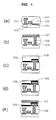
- Figs. 1(a) through 1(e) show, in sectional views, a memory cell in a DRAM for use in a semiconductor integrated circuit device.
- the memory cell is composed of a single MOS transistor and a single capacitor.
- Figs. 1(a) through 1(e) show a process of successively depositing a polysilicon, at least one kind of barrier metal, a high permittivity dielectric, and an upper electrode, after forming a bit line 102, to form a capacitor portion.
- Fig. 1(a) shows, in a sectional view, a transistor for the memory cell.
- a contact hole is opened in the interlayer insulating film 105 by photolithography and plasma etching.
- the polysilicon 106 is formed in the contact hole to extend onto the interlayer film 105 by low-pressure chemical vapor deposition method (hereinafter referred to as "LPCVD").
- LPCVD low-pressure chemical vapor deposition method
- Phosphorus (P) is diffused into the polysilicon so that the polysilicon has a low resistance.
- Tantalum (Ta) and platinum (Pt) are deposited to a thickness of 10 ⁇ 100 nm to form the barrier metal layer 107.
- a high permittivity film 108 made of, for example, SrTiO3 is formed on the entire upper surface by radio-frequency (RF) magnetron sputtering or ion-beam sputtering.
- RF radio-frequency
- the interlayer insulating film 109 is further formed on a substantially entire upper surface, so that the high permittivity film 108 is buried in the interlayer insulating film. Then, the interlayer film 109 is deposited to a thickness enough to flatten the upper surface substantially. If the surface cannot be flattened sufficiently, an organic insulating film having the same etching rate as the interlayer insulating film 109 is applied to flatten the surface completely. In this state, the entire upper surface is etched by plasma etching using a main gas of CF4. The etching is stopped at the point where the surface of the high permittivity film 108 is exposed, thus leaving the interlayer insulating film 109 in place (Fig. 1(d)).
- the upper electrode 110 of titanium nitride (TiN) or aluminum (Al) is formed by plasma-assisted chemical vapor deposition method (hereinafter referred to as "P-CVD") and sputtering, thus completing a capacitor (thin-film capacitor) (Fig. 1(e)).
- P-CVD plasma-assisted chemical vapor deposition method
- sputtering thus completing a capacitor (thin-film capacitor) (Fig. 1(e)
- Figs. 2(a) through 2(e) show, in sectional views, a memory cell in a DRAM for use in a semiconductor integrated circuit device.
- the memory cell is composed of a single MOS transistor and a single capacitor.
- Figs. 2(a) through 2(e) show a process of successively depositing polysilicon, at least one kind of barrier metal layer, a high permittivity dielectric, and an upper electrode, after forming a bit line, to form a capacitor portion.
- reference numeral 201 denotes a word line
- 202 denotes a bit line
- 203 denotes diffused layers corresponding to a source and a drain
- 204 denotes a silicon substrate
- 205 and 209 denote interlayer insulating films
- 206 denotes polysilicon of a lower electrode
- 207 denotes a barrier metal layer
- 208 denotes a high permittivity film made of, e.g., SrTiO3
- 210 denotes an upper electrode.
- Figs. 2(a) and 2(b) show entirely the same steps as in Figs. 1(a) and 1(b) for the first embodiment.
- Fig. 2(c) where the interlayer insulating film 209 is formed on a substantially entire surface, it is deposited in conformity with a profile of the protruding high permittivity film 208. It should be noted that the interlayer insulating film 209 is not required to be deposited as thick as in the first embodiment. In this state, the entire upper surface is etched back by plasma etching using a main gas of CF4, so that the interlayer insulating film 209 remains at only the side and end portions of the lower electrode 206 where the high permittivity film 208 was made thin (Fig. 2(d)).
- the upper electrode 210 of titanium nitride (TiN) and aluminum (Al) is formed by P-CVD method and sputtering so as to cover the high permittivity film 208 and the remained interlayer insulating film 209, thus completing a capacitor (thin-film capacitor) (Fig. 2(e)).
- TiN titanium nitride
- Al aluminum
- Figs. 3(a) through 3(e) like Fig. 1, show, in sectional views, a memory cell in a DRAM for use in a semiconductor integrated circuit device.
- the memory cell is composed of a single MOS transistor and a single capacitor.
- Figs. 3(a) through 3(e) show a process of successively depositing a polysilicon, at least one kind of barrier metal layer, a high permittivity dielectric, and an upper electrode, after forming a bit line, to form a capacitor portion.
- reference numeral 301 denotes a word line
- 302 denotes a bit line
- 303 denotes diffused layers corresponding to a source and a drain
- 304 denotes a silicon substrate
- 305 and 309 denote interlayer insulating films
- 306 denotes polysilicon of a lower electrode
- 307 denotes a barrier metal layer
- 308 denotes a high permittivity film made of, e.g, SrTiO3
- 310 denotes an upper electrode.
- Fig. 3(a) shows a sectional view of the transistor formed for the memory cell.
- a contact hole is opened in the interlayer insulating film 305 by photolithography and plasma etching.
- the polysilicon 306 is formed in the contact hole to extend onto the interlayer insulating film 305 by the LPCVD method.
- Phosphorus (P) is diffused into the polysilicon so that the polysilicon has a low resistance.
- Tantalum (Ta) and platinum (Pt) are deposited to a thickness of 10 ⁇ 100 nm to form the barrier metal layer 307.
- the high permittivity film 308 is deposited on the barrier metal layer 307 by the RF magnetron sputtering or ion-beam sputtering.
- the high permittivity film 308, the barrier metal layer 307 and the polysilicon 306 are worked successively and collectively into a predetermined shape by photolithography and plasma etching, so that they protrude on the surface corresponding to the contact hole. Thereafter, the interlayer insulating film 309 is further formed on a substantially entire upper surface (Fig. 3(c)).
- the interlayer insulating film 309 is deposited to a thickness enough to flatten the surface substantially. If the surface cannot be flattened sufficiently, an organic insulating film having the same etching rate as the interlayer insulating film 309 is applied to flatten the surface completely. In this state, the entire upper surface is etched by plasma etching using a main gas of CF4. The etching is stopped at the point where the surface of the high permittivity film 308 is exposed, thus leaving the interlayer insulating film 309 in place (Fig. 3(d)).
- the upper electrode 310 of titanium nitride (TiN) and aluminum (Al) is formed by P-CVD method and sputtering, thus completing a capacitor (thin-film capacitor) (Fig. 3(e)).
- the capacitor fabricated according to this embodiment is capable of suppressing an occurrence of short-circuiting between the upper electrode and the side or end portions of the lower electrode and suppressing an increase of the leakage current at the end portions of the high permittivity film.
- Figs. 4(a) through 4(e) show, in sectional views, a memory cell in a DRAM for use in a semiconductor integrated circuit device.
- the memory cell is composed of a single MOS transistor and a single capacitor.
- Figs. 4(a) through 4(e) show a process of successively depositing a polysilicon, at least one kind of barrier metal layer, a high permittivity dielectric, and an upper electrode, after forming a bit line, to form a capacitor portion.
- reference numeral 401 denotes a word line
- 402 denotes a bit line
- 403 denotes diffused layers corresponding to a source and a drain
- 404 denotes a silicon substrate
- 405 and 409 denote interlayer insulating films
- 406 denotes polysilicon of a lower electrode
- 407 denotes a barrier metal layer
- 408 denotes a high permittivity film made of, e.g., SrTiO3
- 410 denotes an upper electrode.
- Figs. 4(a) and 4(b) show entirely the same steps as in Figs. 3(a) and 3(b) for the third embodiment, an explanation is not repeated here.
- Fig. 4(c) where the interlayer insulating film 409 is formed on a substantially entire upper surface, it is deposited in conformity with a profile of the protruding high permittivity film 408. It should be noted that the interlayer insulating film 408 is not required to be deposited as thick as in the third embodiment.
- the entire upper surface is etched back by plasma etching using a main gas of CF4, thereby leaving the interlayer insulating film 409 at only the side and end portions of the lower electrode 406 where the high permittivity film 408 was made thin (Fig. 4(d)).
- the upper electrode 410 of titanium nitride (TiN) and aluminum (Al) is formed by P-CVD method and sputtering so as to cover the high permittivity film 408 and the remaining interlayer insulating film 409, thus completing a capacitor (thin-film capacitor) (Fig. 4(e)).
- TiN titanium nitride
- Al aluminum
- the high permittivity film may be made of the material other than SrTiO3 which has been focussed hereinabove.
- the material can be represented by a chemical formula of ABO3 where A contains at least one of Ba, Sr, Pb, La, Li and K, and B contains at least one of Zr, Ti, Ta, Nb, Mg, Mn, Fe, Zn and W.
- the material may be, e.g., (Ba, Sr)TiO3, PbTiO3, Pb(Zr, Ti)O3, (Pb, La)(Zr, Ti)3, Pb(Mg, Nb)O3, Pb(Mg, W)O3, Pb(Zn, Nb)O3, LiTaO3, LiNbO3, KTaO3, KNbO3, etc.
- the material may also be Ta205, Bi4Ti3O12, BaMgF4, etc. which are represented by chemical formulas other than the above.
- the interlayer insulating film can effectively suppress an increase in a leakage current. Further, since the interlayer insulating thin-film, which has a low permittivity, contributes to the capacitor at only the side portions of the lower electrode, the upper surface of the lower electrode can provide a high capacitance density due to the high permittivity film.
- the upper electrode is deposited after the high permittivity film and lower electrode have been etched successively and collectively, it is possible to effectively suppress an occurrence of short-circuiting between the electrodes or an increase in the leakage current at the end portions of the high permittivity film.
Applications Claiming Priority (4)
| Application Number | Priority Date | Filing Date | Title |
|---|---|---|---|
| JP183496/91 | 1991-06-28 | ||
| JP18349691 | 1991-06-28 | ||
| JP246995/91 | 1991-08-31 | ||
| JP3246995A JP2715736B2 (ja) | 1991-06-28 | 1991-08-31 | 半導体装置の製造方法 |
Publications (1)
| Publication Number | Publication Date |
|---|---|
| EP0521676A1 true EP0521676A1 (de) | 1993-01-07 |
Family
ID=26501913
Family Applications (1)
| Application Number | Title | Priority Date | Filing Date |
|---|---|---|---|
| EP92305954A Ceased EP0521676A1 (de) | 1991-06-28 | 1992-06-29 | Dünnschicht-Kapazität in einer integrierten Schaltung eines Halbleiterbauelementes und Verfahren zu ihrer Herstellung |
Country Status (3)
| Country | Link |
|---|---|
| US (1) | US5332684A (de) |
| EP (1) | EP0521676A1 (de) |
| JP (1) | JP2715736B2 (de) |
Cited By (3)
| Publication number | Priority date | Publication date | Assignee | Title |
|---|---|---|---|---|
| DE19518044A1 (de) * | 1994-06-09 | 1995-12-14 | Ibm | Verfahren zur Herstellung von Speicherkondensatoren unter Verwendung von Materialien mit hoher Dielektrizitätskonstante |
| DE19636054A1 (de) * | 1995-09-08 | 1997-03-13 | Toshiba Kawasaki Kk | Halbleitervorrichtung und Verfahren zu deren Herstellung |
| DE19640218A1 (de) * | 1996-09-30 | 1998-04-02 | Siemens Ag | Integrierte Halbleiterspeicheranordnung |
Families Citing this family (11)
| Publication number | Priority date | Publication date | Assignee | Title |
|---|---|---|---|---|
| JP2601022B2 (ja) * | 1990-11-30 | 1997-04-16 | 日本電気株式会社 | 半導体装置の製造方法 |
| JPH0730077A (ja) * | 1993-06-23 | 1995-01-31 | Mitsubishi Electric Corp | 半導体装置およびその製造方法 |
| JP2682392B2 (ja) * | 1993-09-01 | 1997-11-26 | 日本電気株式会社 | 薄膜キャパシタおよびその製造方法 |
| JP3407409B2 (ja) * | 1994-07-27 | 2003-05-19 | 富士通株式会社 | 高誘電率薄膜の製造方法 |
| JP2982855B2 (ja) * | 1994-09-20 | 1999-11-29 | 日本電気株式会社 | 半導体装置とその製造方法 |
| US5751019A (en) * | 1994-12-06 | 1998-05-12 | Varian Associates, Inc. | Method and structure for reducing short circuits between overlapping conductors |
| US5670410A (en) * | 1996-09-25 | 1997-09-23 | Chartered Semiconductor Manufacturing Pte Ltd. | Method of forming integrated CMP stopper and analog capacitor |
| US5981378A (en) | 1997-07-25 | 1999-11-09 | Vlsi Technology, Inc. | Reliable interconnect via structures and methods for making the same |
| KR100600315B1 (ko) * | 2000-06-28 | 2006-07-13 | 주식회사 하이닉스반도체 | 반도체 소자의 캐패시터 제조 방법 |
| US20070212797A1 (en) * | 2006-03-08 | 2007-09-13 | Suk-Hun Choi | Method of forming a ferroelectric device |
| US9536940B2 (en) * | 2012-09-19 | 2017-01-03 | Micron Technology, Inc. | Interfacial materials for use in semiconductor structures and related methods |
Citations (4)
| Publication number | Priority date | Publication date | Assignee | Title |
|---|---|---|---|---|
| EP0046868A2 (de) * | 1980-08-29 | 1982-03-10 | International Business Machines Corporation | Kondensatoranordnung mit doppeltem Dielektrikum |
| EP0338157A2 (de) * | 1988-04-22 | 1989-10-25 | Ramtron International Corporation | DRAM-Zelle mit verstärkter Ladung |
| EP0380326A2 (de) * | 1989-01-26 | 1990-08-01 | Seiko Epson Corporation | Verfahren zur Herstellung einer Halbleitervorrichtung |
| DE4107165A1 (de) * | 1990-04-13 | 1991-10-17 | Mitsubishi Electric Corp | Halbleiterspeicherzelle |
Family Cites Families (1)
| Publication number | Priority date | Publication date | Assignee | Title |
|---|---|---|---|---|
| US5079670A (en) * | 1988-05-03 | 1992-01-07 | Texas Instruments Incorporated | Metal plate capacitor and method for making the same |
-
1991
- 1991-08-31 JP JP3246995A patent/JP2715736B2/ja not_active Expired - Fee Related
-
1992
- 1992-06-29 US US07/905,375 patent/US5332684A/en not_active Expired - Lifetime
- 1992-06-29 EP EP92305954A patent/EP0521676A1/de not_active Ceased
Patent Citations (4)
| Publication number | Priority date | Publication date | Assignee | Title |
|---|---|---|---|---|
| EP0046868A2 (de) * | 1980-08-29 | 1982-03-10 | International Business Machines Corporation | Kondensatoranordnung mit doppeltem Dielektrikum |
| EP0338157A2 (de) * | 1988-04-22 | 1989-10-25 | Ramtron International Corporation | DRAM-Zelle mit verstärkter Ladung |
| EP0380326A2 (de) * | 1989-01-26 | 1990-08-01 | Seiko Epson Corporation | Verfahren zur Herstellung einer Halbleitervorrichtung |
| DE4107165A1 (de) * | 1990-04-13 | 1991-10-17 | Mitsubishi Electric Corp | Halbleiterspeicherzelle |
Non-Patent Citations (1)
| Title |
|---|
| IEEE TRANSACTIONS ON ELECTRON DEVICES. vol. 37, no. 4, April 1990, NEW YORK US pages 972 - 979; S. GI BYEON ET AL: 'High-performance tantalum oxide capacitors fabricated by a novel reoxidation scheme' * |
Cited By (5)
| Publication number | Priority date | Publication date | Assignee | Title |
|---|---|---|---|---|
| DE19518044A1 (de) * | 1994-06-09 | 1995-12-14 | Ibm | Verfahren zur Herstellung von Speicherkondensatoren unter Verwendung von Materialien mit hoher Dielektrizitätskonstante |
| DE19636054A1 (de) * | 1995-09-08 | 1997-03-13 | Toshiba Kawasaki Kk | Halbleitervorrichtung und Verfahren zu deren Herstellung |
| DE19640218A1 (de) * | 1996-09-30 | 1998-04-02 | Siemens Ag | Integrierte Halbleiterspeicheranordnung |
| DE19640218C2 (de) * | 1996-09-30 | 2000-11-02 | Siemens Ag | Integrierte Halbleiterspeicheranordnung mit Speicherkondensatoren |
| US6316802B1 (en) | 1996-09-30 | 2001-11-13 | Infineon Technologies Ag | Easy to manufacture integrated semiconductor memory configuration with platinum electrodes |
Also Published As
| Publication number | Publication date |
|---|---|
| US5332684A (en) | 1994-07-26 |
| JP2715736B2 (ja) | 1998-02-18 |
| JPH0563156A (ja) | 1993-03-12 |
Similar Documents
| Publication | Publication Date | Title |
|---|---|---|
| US5940676A (en) | Scalable high dielectric constant capacitor | |
| US5440157A (en) | Semiconductor integrated-circuit capacitor having a carbon film electrode | |
| US6690052B2 (en) | Semiconductor device having a capacitor with a multi-layer dielectric | |
| KR960005245B1 (ko) | 반도체장치의 제조방법 | |
| US5449630A (en) | Method for fabricating a trench capacitor structure for dynamic random access memory integrated circuit | |
| EP0643395A1 (de) | Speicherkondensator mit einer Elektrode aus einem leitfähigen Oxyd für Metalloxyd-Dielektrika | |
| EP0521676A1 (de) | Dünnschicht-Kapazität in einer integrierten Schaltung eines Halbleiterbauelementes und Verfahren zu ihrer Herstellung | |
| US5742472A (en) | Stacked capacitors for integrated circuit devices and related methods | |
| US5498561A (en) | Method of fabricating memory cell for semiconductor integrated circuit | |
| US5530279A (en) | Thin film capacitor with small leakage current and method for fabricating the same | |
| US5583356A (en) | Connector arrangement for a semiconductor memory device | |
| US5920453A (en) | Completely encapsulated top electrode of a ferroelectric capacitor | |
| KR0144921B1 (ko) | 반도체 메모리소자의 커패시터 구조 및 그 제조방법 | |
| US5459095A (en) | Method for making capacitor for use in DRAM cell using triple layers of photoresist | |
| US20040089891A1 (en) | Semiconductor device including electrode or the like having opening closed and method of manufacturing the same | |
| US6156619A (en) | Semiconductor device and method of fabricating | |
| US6399457B2 (en) | Semiconductor device having capacitor and method of manufacturing the same | |
| US6605505B2 (en) | Process for producing an integrated semiconductor memory configuration | |
| US5837579A (en) | Rugged polysilicon process for DRAM capacitors | |
| EP0978881A2 (de) | Ferroelektrischer Kondensator und Verfahren zur Herstellung | |
| US6821861B1 (en) | Method for fabricating an electrode arrangement for charge storage | |
| EP0716451A1 (de) | Dünnschichtkondensator und Verfahren zu seiner Herstellung | |
| US6051475A (en) | Method for manufacturing a silicide to silicide capacitor | |
| KR0148503B1 (ko) | 반도체 장치의 캐패시터와 그 제조방법 | |
| JPH09129849A (ja) | 半導体素子のキャパシター及びその製造方法 |
Legal Events
| Date | Code | Title | Description |
|---|---|---|---|
| PUAI | Public reference made under article 153(3) epc to a published international application that has entered the european phase |
Free format text: ORIGINAL CODE: 0009012 |
|
| AK | Designated contracting states |
Kind code of ref document: A1 Designated state(s): DE FR GB NL |
|
| 17P | Request for examination filed |
Effective date: 19921129 |
|
| 17Q | First examination report despatched |
Effective date: 19931011 |
|
| APAB | Appeal dossier modified |
Free format text: ORIGINAL CODE: EPIDOS NOAPE |
|
| APAA | Appeal reference recorded |
Free format text: ORIGINAL CODE: EPIDOS REFN |
|
| APAB | Appeal dossier modified |
Free format text: ORIGINAL CODE: EPIDOS NOAPE |
|
| STAA | Information on the status of an ep patent application or granted ep patent |
Free format text: STATUS: THE APPLICATION HAS BEEN REFUSED |
|
| 18R | Application refused |
Effective date: 19961228 |
|
| APAF | Appeal reference modified |
Free format text: ORIGINAL CODE: EPIDOSCREFNE |