EP0521659B1 - Circuit de stabilisation à haute tension pour appareil d'affichage vidéo - Google Patents
Circuit de stabilisation à haute tension pour appareil d'affichage vidéo Download PDFInfo
- Publication number
- EP0521659B1 EP0521659B1 EP92305881A EP92305881A EP0521659B1 EP 0521659 B1 EP0521659 B1 EP 0521659B1 EP 92305881 A EP92305881 A EP 92305881A EP 92305881 A EP92305881 A EP 92305881A EP 0521659 B1 EP0521659 B1 EP 0521659B1
- Authority
- EP
- European Patent Office
- Prior art keywords
- winding
- current
- voltage
- transformer
- retrace
- Prior art date
- Legal status (The legal status is an assumption and is not a legal conclusion. Google has not performed a legal analysis and makes no representation as to the accuracy of the status listed.)
- Expired - Lifetime
Links
- 230000006641 stabilisation Effects 0.000 title description 3
- 238000011105 stabilization Methods 0.000 title description 3
- 238000004804 winding Methods 0.000 claims description 74
- CLSVJBIHYWPGQY-UHFFFAOYSA-N [3-(2,5-dimethylphenyl)-8-methoxy-2-oxo-1-azaspiro[4.5]dec-3-en-4-yl] ethyl carbonate Chemical compound CCOC(=O)OC1=C(C=2C(=CC=C(C)C=2)C)C(=O)NC11CCC(OC)CC1 CLSVJBIHYWPGQY-UHFFFAOYSA-N 0.000 claims description 21
- 230000001105 regulatory effect Effects 0.000 claims description 16
- 238000010168 coupling process Methods 0.000 claims description 2
- 238000005859 coupling reaction Methods 0.000 claims description 2
- 239000003990 capacitor Substances 0.000 description 13
- 230000033228 biological regulation Effects 0.000 description 5
- 230000007423 decrease Effects 0.000 description 5
- 230000002829 reductive effect Effects 0.000 description 4
- 238000004146 energy storage Methods 0.000 description 3
- OKTJSMMVPCPJKN-UHFFFAOYSA-N Carbon Chemical compound [C] OKTJSMMVPCPJKN-UHFFFAOYSA-N 0.000 description 1
- 230000008878 coupling Effects 0.000 description 1
- 230000003247 decreasing effect Effects 0.000 description 1
- 230000002950 deficient Effects 0.000 description 1
- 238000001914 filtration Methods 0.000 description 1
- 230000010354 integration Effects 0.000 description 1
- 230000000670 limiting effect Effects 0.000 description 1
- 230000000873 masking effect Effects 0.000 description 1
- 230000029058 respiratory gaseous exchange Effects 0.000 description 1
- 230000002441 reversible effect Effects 0.000 description 1
- 238000005070 sampling Methods 0.000 description 1
- 238000007493 shaping process Methods 0.000 description 1
- 239000007787 solid Substances 0.000 description 1
Images


Classifications
-
- H—ELECTRICITY
- H04—ELECTRIC COMMUNICATION TECHNIQUE
- H04N—PICTORIAL COMMUNICATION, e.g. TELEVISION
- H04N3/00—Scanning details of television systems; Combination thereof with generation of supply voltages
- H04N3/10—Scanning details of television systems; Combination thereof with generation of supply voltages by means not exclusively optical-mechanical
- H04N3/16—Scanning details of television systems; Combination thereof with generation of supply voltages by means not exclusively optical-mechanical by deflecting electron beam in cathode-ray tube, e.g. scanning corrections
- H04N3/18—Generation of supply voltages, in combination with electron beam deflecting
- H04N3/185—Maintaining dc voltage constant
-
- H—ELECTRICITY
- H04—ELECTRIC COMMUNICATION TECHNIQUE
- H04N—PICTORIAL COMMUNICATION, e.g. TELEVISION
- H04N3/00—Scanning details of television systems; Combination thereof with generation of supply voltages
- H04N3/10—Scanning details of television systems; Combination thereof with generation of supply voltages by means not exclusively optical-mechanical
- H04N3/16—Scanning details of television systems; Combination thereof with generation of supply voltages by means not exclusively optical-mechanical by deflecting electron beam in cathode-ray tube, e.g. scanning corrections
- H04N3/22—Circuits for controlling dimensions, shape or centering of picture on screen
- H04N3/223—Controlling dimensions
Definitions
- the energy storage coil is parallel coupled to a retrace resonant circuit during the energy transfer interval and thus stabilizes also the horizontal retrace time which might have otherwise increased with increasing beam current.
- a regulated power supply embodying a further aspect of the invention includes a retrace resonant circuit that includes a deflection winding.
- a deflection current is generated in the deflection winding, during a deflection cycle and a first pulse is generated in a first winding of a flyback transformer, during retrace.
- a pulse-width-modulator is responsive to a control signal for generating a pulse-width-modulated signal that is modulated in accordance with the control signal.
- a switching arrangement generates a second pulse in the second winding, during retrace, that is modulated in accordance with the modulated signal. Both the first and second pulses are transformer-coupled to a load circuit via the transformer for generating one of a regulated load voltage and a regulated load current in the load circuit.
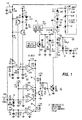
- FIGURE 1 illustrates a horizontal deflection circuit 100 and a high voltage stabilization or regulator circuit 102, embodying an aspect of the invention, that generates a stabilized ultor voltage U.
- the arrangement of FIGURE 1 may be used in conjunction with, for example, a 37" color picture tube, not shown, of the type Mitsubishi A89JKA81X.
- east-west raster correction, horizontal linearity correction and component values which are not relevant for explaining the invention, are omitted from FIGURE 1.
- a switching transistor Q1 of deflection circuit 100 responsive to a horizontal rate drive signal, generates a horizontal rate retrace voltage V1.
- Voltage V1 is generated in a deflection retrace or flyback resonant circuit 79.
- Voltage V1 is coupled via a primary winding W1 of a flyback transformer T1 to a high voltage winding W2 to form a horizontal rate retrace or flyback high voltage VW2 in each winding portion of winding W2.
- Circuit 79 includes a deflection winding LH in which a deflection current iy is generated.
- Rectifying diodes, DHV coupled in a diode-split configuration to the winding portions of winding W2, produce an ultor voltage U that is coupled to the anode of the picture tube, not shown.
- FIGURES 2a-2e and 3a-3f illustrate waveforms useful for the explanation of the circuit of FIGURE 1. Similar symbols and numerals in FIGURES 1, 2a-2e and 3a-3f indicate similar items or functions.
- the waveforms of FIGURES 2a-2e are drawn in solid lines for 0.2 mA average beam current beam and in broken lines for 1.2 mA average beam current.
- left FIGURES 2a and 2b The waveforms on the left hand side of FIGURES 2a and 2b, referred to herein as left FIGURES 2a and 2b, respectively, are used to explain the operation when high voltage regulator circuit 102 is disabled.
- retrace voltage V1 of FIGURE 1 decreases at high beam current, as shown in broken line, and the retrace time tends to increase.
- An interval tc indicates the conduction interval of high voltage rectifying diodes DHV integrated in winding W2 of flyback transformer T1. Interval tc is negligibly small at low beam currents, as shown in left FIGURE 2a, but increases at high beam currents because of the leakage inductance between windings W1 and W2 of FIGURE 1.
- ultor voltage U decreases significantly from 28.5 to 25.9KV.
- the high voltage level U is equal approximately to the retrace voltage at the center of interval tc, at left FIGURE 2a.
- the slopes of a primary current il of left FIGURE 2b are determined by a supply voltage B+ of FIGURE 1 that is coupled to winding W1, the inductance of winding W1 and the retrace resonant frequency of circuit 79.
- Voltage B+ is coupled to the undotted terminal of winding W1.
- Voltage B+ is supplied by a voltage regulator 66.
- Current il increases to a peak amplitude of 1.7A at high beam current. The increase appears as an added D.C. component causing the negative portion of current il to decrease.
- DQ1 damper diode
- Excessive D.C. component may lead to an improper operation causing deflection distortions and a reduction of the high voltage.
- high voltage regulator circuit 102 includes an energy storage coil or inductor L1, a diode D1 and a winding W3 of transformer T1 coupled in series with a collector-emitter current path of a switching transistor Q2 that is controlled by a control circuit 103.
- Diode D1 is conductive during a controllable portion of trace.
- a snubber network that includes a capacitor C7 and a resistor R20 across coil L1 prevents excessive ringing when diode D1 cuts-off during the retrace interval.
- the waveforms of right FIGURES 2a-2e are used for explaining the normal operation of high voltage regulator circuit 102.
- winding W3 of FIGURE 1 is also employed in a retrace voltage power supply that includes a rectifier D2, a current limiting resistor R4 and a filter capacitor C2 to obtain a supply voltage in capacitor C2 for energizing video output amplifiers, not shown.
- a high voltage representative voltage is developed at the emitter of transistor Q3 that is coupled to a voltage divider.
- the voltage divider further includes a bleeder resistor BLEEDER.
- a control circuit 103 generates a base drive voltage V3 of transistor Q2, having a waveform of FIGURE 2d.
- a leading edge LE of voltage V3, that causes transistor Q2 to begin conducting is phase-modulated in accordance with the voltage across resistor R1, in an interval t1-t2 that occurs during trace.
- the voltage across resistor R1 varies when ultor voltage U varies.
- Transistor Q2 of FIGURE 1 conducts at low beam current or at high ultor voltage U, during an interval t2-t6 of FIGURE 2d, as shown in solid line.
- each of transformer T1, coil L1 and deflection winding LH is transferred as a retrace current flow into a capacitor CR of circuit 79 of FIGURE 1 during the first half of the retrace interval to produce a retrace voltage V1 of right FIGURE 2a.
- Current i2 flowing through winding W3 is a down-ramping current because of the positive retrace voltage V2 at the dotted terminal of winding W3.
- Current i2 reaches a zero level at time t5 of FIGURE 2c.
- Diode D1 of FIGURE 1 is then reverse biased by retrace voltage V2 and decouples coil L1 from winding W3.
- coil L1 is parallel-coupled to retrace circuit 79, as long as down-ramping current i2 flows.
- a trace voltage VCS developed across a trace capacitor CS that is coupled in series with deflection winding LH, has a D.C. voltage component that is equal to voltage B+.
- the D.C. voltage component of voltage VCS is substantially unaffected by variation of the conduction interval of transistor Q2 of circuit 102.
- Deflection current iy is regulated in accordance with the D.C. voltage component of voltage VCS that is determined by voltage B+.
- Voltage B+ is regulated independently of the operation of high voltage regulator circuit 102.
- the retrace frequency increases during current i2 conduction interval, t3-t5 of FIGURE 2c, to compensate for retrace time modulation that is caused by beam current variations. Therefore, voltage V1 of right FIGURE 2a increases faster at high beam current than at low beam current, as shown by the difference between the solid and broken lines.
- the additional energy transferred from coil L1 of FIGURE 1 produces a higher peak amplitude of voltage V1 at high beam current than at low beam current.
- the decrease in high voltage U is smaller at high beam current and the retrace time remains constant.
- Circuit 103 produces pulse-width-modulated voltage V3 that controls transistor Q2.
- a low voltage end of bleeder resistor BLEEDER is coupled to a filter capacitor C1, and via, resistor R1, to an emitter of a transistor Q3.
- a biasing network that includes a resistor R7, a diode D4, a zener diode D5 and a resistor R8 provides a stable reference base voltage of transistor Q3 and an emitter voltage of a transistor Q4.
- a bleeder current in resistor R1 is split into a greater portion that flows through a series arrangement of a resistor R2, a resistor R3, a resistor R5 and a flyback transformer winding, not shown, of transformer T1 to ground. That flyback winding in the current path of resistors R2, R3 and R5 generates a 250 Vpp negative going retrace pulse at a terminal 103a.
- the voltage at terminal 103a represents ground potential.
- the retrace pulses at terminal 103a are integrated by an integration network that includes resistor R5 and a capacitor C3 to produce a sawtooth voltage V4.
- the other, and smaller, portion of the bleeder current flows through transistor Q3 and through a beam current sampling load resistor R6.
- a high voltage representative voltage V5 developed across resistor R6 is filtered by a capacitor C4.
- voltage V4 across resistor R5 is not modulated by high voltage variations because the emitter of transistor Q3 is at a constant D.C. potential.
- Voltage V5 varies with ultor voltage variations, as shown in FIGURE 3b.
- the current that flows through resistors R2, R3 and R5 reduces the D.C. level of voltage V5, thus enabling the usage of a higher value resistor for resistor R6.
- Voltage V4 is compared with voltage V5 by a voltage comparator U1A for modulating a trailing edge of voltage V9 during an interval t1-t2 of FIGURE 3f.
- Comparators U1B and U1C of FIGURE 1 are driven by retrace pulse voltage V6 to hold down output voltages V8 and V9 of comparators U1B and U1C, respectively, during retrace.
- a comparator U1D is driven by a sawtooth voltage V7 of FIGURE 3d produced by an R-C network of a resistor R10 of FIGURE 1 and a capacitor C5. Output voltage V8 prevents transistor Q2 from being turned on during the first half of the trace interval.
- Voltages V8 and V9 are summed via resistors R16 and R15 to drive a base of a transistor Q5.
- Transistor Q5 produces, at its collector, voltage V3 that is also developed at the base of transistor Q2.
- High voltage U is adjusted by a variable resistor R3 which varies in a differential manner the D.C. levels of voltages V4 and V5.
- Transistor Q4 provides protection by disabling circuit 103 and transistor Q2.
- transistor Q3 becomes disabled or nonconductive and transistor Q4 becomes conductive.
- the current flowing through resistor R7, diode D4 and transistor Q4 charges capacitor C4 to a higher voltage than voltage V4, causing the sum of voltages V8 and V9 to be positive during trace.
- transistor Q2 cannot conduct during trace and current i2 is zero.
- the protection operation provides a soft start-up operation because the high voltage regulator is disabled until high voltage U is equal to at least 70% of its nominal value.
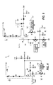
- FIGURE 4 illustrates a high voltage regulator 102', embodying another aspect of the invention. Similar symbols and numerals in FIGURES 1 and 4, with the exception of the symbol (') in FIGURE 4, indicate similar items or functions.
- Series coupled diode D1', inductor L1' and transistor Q2' of FIGURE 4 are coupled to a winding W3' which supplies negative going retrace pulses. Winding W3' is also used as a voltage source for a trace rectifier D2', for producing in a capacitor C2' a supply voltage of 28 volts required by, for example, a vertical deflection amplifier, not shown.
- an E-W raster distortion corrected horizontal deflection circuit 200 is included.
- An E-W switching transistor Q11 of FIGURE 5 is conductive and supplies a controllable amount of energy to deflection resonant circuit 79" during a first portion of the retrace interval for obtaining an East-West amplitude modulated deflection current.
- Horizontal retrace begins when transistor Q1" is turned off.
- Transistor Q11 is maintained conductive from a time at the beginning of the horizontal trace interval and until a controllable instant during the first portion of horizontal retrace .
- the retrace, first portion begins at the time transistor Q1" becomes nonconductive.
- the length of the first portion varies in a vertical rate manner to provide East-West raster distortion correction.
- transistor Q11 Following the retrace, first portion, transistor Q11 becomes nonconductive and isolates a flyback resonant circuit 251, that includes winding W1" and a flyback capacitance CT, from resonant circuit 79".
- High voltage regulation circuit 102" is also isolated from retrace circuit 79", during a second portion of the retrace interval, when diodes DHV are conductive. As a result, circuit 102" is not by-passed by circuit 79". Therefore, the efficiency of circuit 102" is, advantageously, increased.
Landscapes
- Engineering & Computer Science (AREA)
- Multimedia (AREA)
- Signal Processing (AREA)
- Details Of Television Scanning (AREA)
- Television Receiver Circuits (AREA)
Claims (14)
- Alimentation régulée pour un dispositif d'affichage vidéo comportant :un circuit résonnant de retour (79) comportant une bobine de déviation (LH),un transformateur de retour (T1),une source (66) de tension d'entrée (B+) raccordée à un premier enroulement (W1) dudit transformateur,un premier dispositif de commutation (Q1) raccordé à ladite bobine de déviation et audit transformateur qui, en fonction dudit signal d'entrée, génère un courant de déviation (iy) dans ladite bobine de déviation au cours d'un cycle de déviation et une première impulsion (V1) dans le premier enroulement dudit transformateur pendant le retour,une source de signal d'entrée de synchronisation à une fréquence en relation avec la fréquence de déviation qui est raccordée à la base dudit premier dispositif de commutation (Q1),un modulateur de largeur d'impulsion (103) qui, en fonction d'un signal de commande (V4), génère un signal modulé en largeur d'impulsions (V3), modulé en fonction dudit signal de commande, caractérisé parun second dispositif de commutation (Q2, D1) raccordé à un second enroulement (W3) dudit transformateur et qui, en fonction dudit signal modulé en largeur d'impulsions, génère une seconde impulsion dans ledit second enroulement, pendant le retour, qui est modulée en fonction dudit signal modulé, ladite première impulsion et ladite seconde impulsion étant couplées par l'intermédiaire du transformateur à un circuit de charge (ANODE) afin de générer l'une des tensions de charge régulée (U) et un courant de charge régulé (iBEAM) dans ledit circuit de charge, etune inductance (L1) raccordée audit second enroulement et formant un circuit pour le courant qui génère un courant (i2) dans ledit second enroulement, dont la vitesse de variation au cours de l'aller du balayage est déterminée par la valeur de ladite inductance et modulée en fonction dudit signal modulé en largeur d'impulsions.
- Alimentation selon la revendication 1 caractérisé par le fait que ledit premier dispositif de commutation (Q1) applique ladite tension d'entrée (B+) à travers ledit premier enroulement (W1) dudit transformateur (T1) pour coupler à travers le transformateur ladite tension d'entrée audit second enroulement pendant l'aller du balayage, afin de générer une tension dans ledit second enroulement qui produit dans ladite inductance (L1) le courant dudit second enroulement (i2).
- Alimentation selon la revendication 2 caractérisée par le fait que ledit second enroulement (W3) est alimenté uniquement par l'intermédiaire dudit transformateur (T1).
- Alimentation selon la revendication 1 caractérisée par le fait que le courant dudit second enroulement (i2) est couplé par l'intermédiaire du transformateur audit circuit de charge (ANODE) pendant le retour.
- Alimentation selon la revendication 1 caractérisée par le fait que ladite première impulsion (V1) est couplée par l'intermédiaire du transformateur à un enroulement haute tension (W2) dudit transformateur (T1), auquel ledit enroulement haute tension est raccordé un redresseur (DHV) pour la génération, à partir de ladite première impulsion, d'une très haute tension (U) et d'un courant de faisceau (iBEAM).
- Alimentation selon la revendication 5 caractérisée par le fait que ledit modulateur à largeur d'impulsions (103) régule la très haute tension par contre-réaction en fonction de ladite très haute tension (U) ou du courant (iBEAM) qui circule à travers ledit enroulement haute tension.
- Alimentation selon la revendication 1 caractérisée par le fait que la modulation dudit signal modulé en largeur d'impulsions (V3) n'a pas d'influence sur ledit courant de déviation (iy).
- Alimentation selon la revendication 1 caractérisée par le fait que ladite tension d'alimentation d'entrée (B+) génère un courant (il) dans ledit premier enroulement (W1) dudit transformateur (T1) afin de stocker de l'énergie magnétique dans ledit transformateur pendant l'aller du balayage, l'énergie stockée servant à compenser les pertes d'énergie dans ledit circuit résonant de retour (79) dans ledit circuit de recharge (ANODE) pendant le retour.
- Alimentation selon la revendication 1 caractérisée par le fait que ledit signal modulé en largeur d'impulsions (V3) est modulé pendant la période d'aller du balayage.
- Alimentation selon la revendication 1 caractérisée par une inductance (L1) raccordée audit second enroulement (W3) dudit transformateur (T1) qui conduit dans ladite inductance un second courant en forme de rampe (I2) dont l'amplitude crête est modulée en fonction du courant de faisceau (iBEAM), où ledit second dispositif de commutation (Q2) découple ladite inductance dudit transformateur pendant une première portion (t5-t6, figure 2b) de l'intervalle de retour (t3-t6) et couple ladite inductance audit transformateur pendant une seconde portion (t3-t5) dudit intervalle de retour et où la longueur desdites première et seconde portions varient en fonction dudit courant de faisceau (iBEAM).
- Alimentation selon la revendication 10 caractérisée par le fait que ladite inductance (L1) est placée dans le circuit de courant du courant dudit second enroulement (i2) et raccordée par l'intermédiaire dudit transformateur (T1) audit circuit résonnant de retour (79) afin de faire varier la fréquence de résonance de retour dudit circuit résonant de retour conformément audit courant de faisceau (iBEAM) de manière à compenser la modulation de durée du retour causée par la variation dudit courant de faisceau.
- Alimentation selon la revendication 1 caractérisée par le fait que ledit second dispositif de commutation (Q2, D1) comporte un redresseur à deux bornes (D1).
- Alimentation selon la revendication 1 caractérisée par le fait que ledit modulateur de largeur d'impulsion (103) fait varier la largeur des impulsions dudit signal modulé (V3) en fonction soit du courant de charge, soit de la tension (U).
- Alimentation selon la revendication 1 caractérisée par le fait que ledit courant de déviation (iy) est régulé en fonction de ladite tension d'alimentation d'entrée (B+) et n'est pas affecté par la modulation à largeur d'impulsion.
Priority Applications (1)
| Application Number | Priority Date | Filing Date | Title |
|---|---|---|---|
| EP98113323A EP0876054B1 (fr) | 1991-07-01 | 1992-06-25 | Circuit de stabilisation à haute tension pour appareil d'affichage vidéo |
Applications Claiming Priority (4)
| Application Number | Priority Date | Filing Date | Title |
|---|---|---|---|
| GB919114168A GB9114168D0 (en) | 1991-07-01 | 1991-07-01 | High voltage regulator |
| GB9114168 | 1991-07-01 | ||
| US07/843,341 US5249160A (en) | 1991-09-05 | 1992-02-28 | SRAM with an address and data multiplexer |
| US843341 | 1992-02-28 |
Related Child Applications (2)
| Application Number | Title | Priority Date | Filing Date |
|---|---|---|---|
| EP98113323A Division EP0876054B1 (fr) | 1991-07-01 | 1992-06-25 | Circuit de stabilisation à haute tension pour appareil d'affichage vidéo |
| EP98113323.4 Division-Into | 1998-07-17 |
Publications (3)
| Publication Number | Publication Date |
|---|---|
| EP0521659A2 EP0521659A2 (fr) | 1993-01-07 |
| EP0521659A3 EP0521659A3 (fr) | 1994-04-27 |
| EP0521659B1 true EP0521659B1 (fr) | 1999-02-03 |
Family
ID=26299162
Family Applications (2)
| Application Number | Title | Priority Date | Filing Date |
|---|---|---|---|
| EP92305881A Expired - Lifetime EP0521659B1 (fr) | 1991-07-01 | 1992-06-25 | Circuit de stabilisation à haute tension pour appareil d'affichage vidéo |
| EP98113323A Expired - Lifetime EP0876054B1 (fr) | 1991-07-01 | 1992-06-25 | Circuit de stabilisation à haute tension pour appareil d'affichage vidéo |
Family Applications After (1)
| Application Number | Title | Priority Date | Filing Date |
|---|---|---|---|
| EP98113323A Expired - Lifetime EP0876054B1 (fr) | 1991-07-01 | 1992-06-25 | Circuit de stabilisation à haute tension pour appareil d'affichage vidéo |
Country Status (5)
| Country | Link |
|---|---|
| EP (2) | EP0521659B1 (fr) |
| JP (1) | JP3372270B2 (fr) |
| DE (2) | DE69228339T2 (fr) |
| MY (1) | MY110569A (fr) |
| SG (1) | SG93770A1 (fr) |
Families Citing this family (3)
| Publication number | Priority date | Publication date | Assignee | Title |
|---|---|---|---|---|
| US6115085A (en) * | 1998-06-19 | 2000-09-05 | Thomson Licensing S.A. | Focus voltage tracking circuit |
| US6252361B1 (en) * | 1999-10-15 | 2001-06-26 | Thomson Licensing S.A. | High-voltage power supply disabling circuit for video display |
| CN102427345B (zh) * | 2011-10-13 | 2014-04-02 | 吉林大学 | 电流脉冲上升沿和下降沿加速装置及加速方法 |
Family Cites Families (9)
| Publication number | Priority date | Publication date | Assignee | Title |
|---|---|---|---|---|
| US4298829A (en) * | 1980-02-08 | 1981-11-03 | Rca Corporation | Power supply and deflection circuit with raster size compensation |
| US4318036A (en) * | 1980-11-10 | 1982-03-02 | Zenith Radio Corporation | Pulse width modulator for a television receiver |
| GB2135859B (en) * | 1983-02-21 | 1986-11-26 | Rca Corp | Picture size control circuit |
| GB8317970D0 (en) * | 1983-07-01 | 1983-08-03 | Rca Corp | Television receiver load compensation circuit |
| US4645990A (en) * | 1985-07-30 | 1987-02-24 | Rca Corporation | High voltage control circuit for video display apparatus |
| FI90174C (fi) * | 1987-10-23 | 1993-12-27 | Rca Licensing Corp | Hoegspaenningsstabiliseringskrets foer en videodisplayapparat |
| CA1300744C (fr) * | 1988-03-25 | 1992-05-12 | Peter Eduard Haferl | Ensemble servant a reduire le courant d'appel dans un transformateur de retour |
| US4866525A (en) * | 1988-11-01 | 1989-09-12 | Thomson Consumer Electronics, Inc. | Television apparatus power supply |
| US5010281A (en) * | 1990-04-30 | 1991-04-23 | Rca Licensing Corporation | High voltage stabilization circuit for video display apparatus |
-
1992
- 1992-06-25 DE DE69228339T patent/DE69228339T2/de not_active Expired - Fee Related
- 1992-06-25 EP EP92305881A patent/EP0521659B1/fr not_active Expired - Lifetime
- 1992-06-25 EP EP98113323A patent/EP0876054B1/fr not_active Expired - Lifetime
- 1992-06-25 SG SG9602501A patent/SG93770A1/en unknown
- 1992-06-25 DE DE69233665T patent/DE69233665T2/de not_active Expired - Fee Related
- 1992-06-30 MY MYPI92001096A patent/MY110569A/en unknown
- 1992-06-30 JP JP19778292A patent/JP3372270B2/ja not_active Expired - Fee Related
Also Published As
| Publication number | Publication date |
|---|---|
| MY110569A (en) | 1998-08-29 |
| JPH05244537A (ja) | 1993-09-21 |
| DE69233665D1 (de) | 2006-12-07 |
| SG93770A1 (en) | 2003-01-21 |
| JP3372270B2 (ja) | 2003-01-27 |
| EP0876054A3 (fr) | 1999-08-04 |
| EP0876054B1 (fr) | 2006-10-25 |
| EP0521659A3 (fr) | 1994-04-27 |
| EP0521659A2 (fr) | 1993-01-07 |
| DE69228339D1 (de) | 1999-03-18 |
| EP0876054A2 (fr) | 1998-11-04 |
| DE69233665T2 (de) | 2007-03-08 |
| DE69228339T2 (de) | 1999-06-17 |
Similar Documents
| Publication | Publication Date | Title |
|---|---|---|
| US4429257A (en) | Variable horizontal deflection circuit capable of providing east-west pincushion correction | |
| US5010281A (en) | High voltage stabilization circuit for video display apparatus | |
| EP0581154B1 (fr) | Circuit de correction de la distorsion d'image | |
| EP0414184A2 (fr) | Circuit de réglage haute tension pour tubes d'image | |
| US5266871A (en) | High voltage stabilization circuit for video display apparatus | |
| US4906902A (en) | Raster distortion corrected deflection circuit | |
| EP0521659B1 (fr) | Circuit de stabilisation à haute tension pour appareil d'affichage vidéo | |
| US5463290A (en) | Power supply stabilization circuit with separate AC/DC negative feedback paths | |
| EP0240142B1 (fr) | Circuit de positionnement de trame pour un système de déflection | |
| US4829216A (en) | SCR regulator for a television apparatus | |
| JP3128651B2 (ja) | 偏向制御回路 | |
| US4572993A (en) | Television deflection circuit with raster width stabilization | |
| JP3795427B2 (ja) | ラスタ歪み補正付き偏向装置 | |
| JP2596824B2 (ja) | テレビジョン偏向装置 | |
| US4794307A (en) | Raster distortion correction for a deflection circuit | |
| EP0313391B1 (fr) | Alimentation en haute tension pour des appareils vidéo | |
| JP3056490B2 (ja) | 偏向装置 | |
| CA1292560C (fr) | Stabilisateur de haute tension pour appareil de television | |
| EP0370660A2 (fr) | Circuit de protection du bloc d'alimentation | |
| JP3479089B2 (ja) | テレビジョン偏向装置 | |
| JP3120850B2 (ja) | テレビジョン装置の電源 | |
| US4812720A (en) | High voltage stabilization circuit for video display apparatus | |
| EP0266996B2 (fr) | Circuit de correction de trame | |
| JPH07254996A (ja) | 水平偏向回路 |
Legal Events
| Date | Code | Title | Description |
|---|---|---|---|
| PUAI | Public reference made under article 153(3) epc to a published international application that has entered the european phase |
Free format text: ORIGINAL CODE: 0009012 |
|
| AK | Designated contracting states |
Kind code of ref document: A2 Designated state(s): DE GB IT |
|
| PUAL | Search report despatched |
Free format text: ORIGINAL CODE: 0009013 |
|
| AK | Designated contracting states |
Kind code of ref document: A3 Designated state(s): DE GB IT |
|
| 17P | Request for examination filed |
Effective date: 19941027 |
|
| 17Q | First examination report despatched |
Effective date: 19961203 |
|
| GRAG | Despatch of communication of intention to grant |
Free format text: ORIGINAL CODE: EPIDOS AGRA |
|
| GRAG | Despatch of communication of intention to grant |
Free format text: ORIGINAL CODE: EPIDOS AGRA |
|
| GRAH | Despatch of communication of intention to grant a patent |
Free format text: ORIGINAL CODE: EPIDOS IGRA |
|
| GRAH | Despatch of communication of intention to grant a patent |
Free format text: ORIGINAL CODE: EPIDOS IGRA |
|
| GRAA | (expected) grant |
Free format text: ORIGINAL CODE: 0009210 |
|
| AK | Designated contracting states |
Kind code of ref document: B1 Designated state(s): DE GB IT |
|
| REF | Corresponds to: |
Ref document number: 69228339 Country of ref document: DE Date of ref document: 19990318 |
|
| ITF | It: translation for a ep patent filed | ||
| PLBE | No opposition filed within time limit |
Free format text: ORIGINAL CODE: 0009261 |
|
| STAA | Information on the status of an ep patent application or granted ep patent |
Free format text: STATUS: NO OPPOSITION FILED WITHIN TIME LIMIT |
|
| 26N | No opposition filed | ||
| REG | Reference to a national code |
Ref country code: GB Ref legal event code: 732E |
|
| REG | Reference to a national code |
Ref country code: GB Ref legal event code: IF02 |
|
| REG | Reference to a national code |
Ref country code: GB Ref legal event code: 746 Effective date: 20030228 |
|
| PGFP | Annual fee paid to national office [announced via postgrant information from national office to epo] |
Ref country code: IT Payment date: 20060630 Year of fee payment: 15 |
|
| PGFP | Annual fee paid to national office [announced via postgrant information from national office to epo] |
Ref country code: DE Payment date: 20070628 Year of fee payment: 16 |
|
| PGFP | Annual fee paid to national office [announced via postgrant information from national office to epo] |
Ref country code: GB Payment date: 20070510 Year of fee payment: 16 |
|
| GBPC | Gb: european patent ceased through non-payment of renewal fee |
Effective date: 20080625 |
|
| PG25 | Lapsed in a contracting state [announced via postgrant information from national office to epo] |
Ref country code: DE Free format text: LAPSE BECAUSE OF NON-PAYMENT OF DUE FEES Effective date: 20090101 |
|
| PG25 | Lapsed in a contracting state [announced via postgrant information from national office to epo] |
Ref country code: GB Free format text: LAPSE BECAUSE OF NON-PAYMENT OF DUE FEES Effective date: 20080625 |
|
| PG25 | Lapsed in a contracting state [announced via postgrant information from national office to epo] |
Ref country code: IT Free format text: LAPSE BECAUSE OF NON-PAYMENT OF DUE FEES Effective date: 20070625 |