EP0520331A2 - Horizontalablenkschaltung mit einem Treibertransformator - Google Patents
Horizontalablenkschaltung mit einem Treibertransformator Download PDFInfo
- Publication number
- EP0520331A2 EP0520331A2 EP92110377A EP92110377A EP0520331A2 EP 0520331 A2 EP0520331 A2 EP 0520331A2 EP 92110377 A EP92110377 A EP 92110377A EP 92110377 A EP92110377 A EP 92110377A EP 0520331 A2 EP0520331 A2 EP 0520331A2
- Authority
- EP
- European Patent Office
- Prior art keywords
- driver
- transistor
- current
- transformer
- driver transformer
- Prior art date
- Legal status (The legal status is an assumption and is not a legal conclusion. Google has not performed a legal analysis and makes no representation as to the accuracy of the status listed.)
- Granted
Links
- 238000004804 winding Methods 0.000 claims abstract description 14
- 230000000903 blocking effect Effects 0.000 claims abstract description 12
- 238000010408 sweeping Methods 0.000 abstract 1
- 238000010586 diagram Methods 0.000 description 12
- 230000010355 oscillation Effects 0.000 description 8
- 230000005540 biological transmission Effects 0.000 description 3
- 230000000694 effects Effects 0.000 description 2
- 230000002411 adverse Effects 0.000 description 1
- 239000003990 capacitor Substances 0.000 description 1
- 230000015556 catabolic process Effects 0.000 description 1
- 238000006731 degradation reaction Methods 0.000 description 1
- 238000000034 method Methods 0.000 description 1
Images
Classifications
-
- H—ELECTRICITY
- H03—ELECTRONIC CIRCUITRY
- H03K—PULSE TECHNIQUE
- H03K17/00—Electronic switching or gating, i.e. not by contact-making and –breaking
- H03K17/04—Modifications for accelerating switching
- H03K17/041—Modifications for accelerating switching without feedback from the output circuit to the control circuit
- H03K17/0412—Modifications for accelerating switching without feedback from the output circuit to the control circuit by measures taken in the control circuit
- H03K17/04126—Modifications for accelerating switching without feedback from the output circuit to the control circuit by measures taken in the control circuit in bipolar transistor switches
-
- H—ELECTRICITY
- H03—ELECTRONIC CIRCUITRY
- H03K—PULSE TECHNIQUE
- H03K17/00—Electronic switching or gating, i.e. not by contact-making and –breaking
- H03K17/51—Electronic switching or gating, i.e. not by contact-making and –breaking characterised by the components used
- H03K17/56—Electronic switching or gating, i.e. not by contact-making and –breaking characterised by the components used by the use, as active elements, of semiconductor devices
- H03K17/60—Electronic switching or gating, i.e. not by contact-making and –breaking characterised by the components used by the use, as active elements, of semiconductor devices the devices being bipolar transistors
- H03K17/605—Electronic switching or gating, i.e. not by contact-making and –breaking characterised by the components used by the use, as active elements, of semiconductor devices the devices being bipolar transistors with galvanic isolation between the control circuit and the output circuit
- H03K17/61—Electronic switching or gating, i.e. not by contact-making and –breaking characterised by the components used by the use, as active elements, of semiconductor devices the devices being bipolar transistors with galvanic isolation between the control circuit and the output circuit using transformer coupling
-
- H—ELECTRICITY
- H03—ELECTRONIC CIRCUITRY
- H03K—PULSE TECHNIQUE
- H03K4/00—Generating pulses having essentially a finite slope or stepped portions
- H03K4/06—Generating pulses having essentially a finite slope or stepped portions having triangular shape
- H03K4/08—Generating pulses having essentially a finite slope or stepped portions having triangular shape having sawtooth shape
- H03K4/48—Generating pulses having essentially a finite slope or stepped portions having triangular shape having sawtooth shape using as active elements semiconductor devices
- H03K4/60—Generating pulses having essentially a finite slope or stepped portions having triangular shape having sawtooth shape using as active elements semiconductor devices in which a sawtooth current is produced through an inductor
- H03K4/62—Generating pulses having essentially a finite slope or stepped portions having triangular shape having sawtooth shape using as active elements semiconductor devices in which a sawtooth current is produced through an inductor using a semiconductor device operating as a switching device
Definitions
- the invention relates to a horizontal deflection circuit of the type specified in the preamble of claim 1.
- the line-end stage transistor of such a horizontal deflection circuit is provided to supply the deflection coils for the horizontal beam deflection of a television tube with the necessary deflection currents.
- a horizontal deflection circuit according to the preamble of claim 1 is known for example from the patent DE 30 44 907 C2.
- the known horizontal deflection circuit contains a driver transistor controlled by a line frequency oscillator, in the collector circuit of which the primary winding of a driver transformer is arranged.
- the secondary winding of this driver transformer forms with the base circuit of a line end stage transistor of this horizontal deflection circuit and a current limiting resistor a control circuit for the line end stage transistor, in each of the oscillation periods of the line deflection oscillation in the blocking phase of the driver transistor Control current flows.
- the line-end stage transistor requires a relatively high control power which only the driver transformer has to deliver during the blocking phase of the driver transistor and which the driver transformer has to absorb from the power supply within one oscillation period of the horizontal deflection oscillation during the current flow phase. This requires a considerable size of the driver transformer and a relatively high driver current.
- the use of such a flyback converter as a driver stage for a horizontal deflection circuit brings with it some problems which are primarily associated with the high magnetic energy which is converted by the flyback converter in one oscillation period.
- the high magnetic energy causes settling and, in particular, settling times, which are large compared to the period of the horizontal deflection vibrations. This is noticeable, for example, when changing an operating state of the television set, for example from standby mode to receiving mode and vice versa, and leads to high peak currents in the control circuit of the line output stage transistor, which can endanger it.
- the invention has for its object to provide a line deflection circuit with a driver transformer such that the settling and decay times of the driver stage is less than the period of the line deflection oscillation, without adversely affecting the high efficiency of the driver stage and the low circuit complexity.
- the driver stage By designing the driver stage as a forward converter, the driver stage only has to be dimensioned to cover the loss energies of the flow losses of the driver current in the control circuit of the line end stage transistor and to cover the removal of the electrical base charge of the line end stage transistor.
- this requires an energy transmission of a significantly lower magnetic energy than with the flyback converter. This significantly lower amount of magnetic energy per oscillation period requires not only a much smaller size of the transformer, but also easier handling of this energy and better defined transmission times of this energy.
- the working circuit of the driver transistor contains a so-called relief network, which protects the driver transistor against impermissibly high current surges or voltage peaks.
- this relief network can be designed such that it takes over the current generated by the driver transformer in the off state of the driver transistor when the clearing current is interrupted. It is particularly advantageous to dimension the driver stage such that the magnetic energy stored in the driver transformer during a leading phase of the driver transistor is completely reduced again within the blocking phase of the driver transistor following the leading phase.
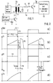
- FIG. 1 shows a circuit diagram of a horizontal deflection circuit with a driver transistor 1, which is controlled by a line frequency oscillator 2.
- the working circuit 3 of the driver transistor is connected to a supply voltage U V of a supply voltage source, not shown in detail, and essentially contains the primary winding 4 of a driver transformer 5, the secondary winding 6 of which is part of the control circuit 7 of a line-end stage transistor 8 of the horizontal deflection circuit.
- the control circuit also contains a limiting resistor 9 for limiting the control current I2 generated by the secondary voltage U2 of the driver transformer for control in the base-emitter path of the line end stage transistor 8.
- This control current I2 controls the deflection current I H that the line end stage transistor 8 for the circuit 10 of the deflection coils is based on of the control current I2 generated.
- an operating current I1 flows through the primary winding 4 of the driver transformer 5.
- a relief network 11 is connected to the primary winding 4 of the driver transistor Protect driver transistor from excessive voltage peaks.
- Diagram a) shows the square wave 12 generated by the line frequency oscillator 2, which controls the driver transistor 1 at its base and whose pulse duration T12 is equal to half the oscillation period T H of the square wave 12 of the line frequency oscillator 2.
- the pulses 12.1 of the square wave voltage 12 control the driver transistor 1 in its saturation state, in which it is completely current-conducting and serves as a switch for the primary winding 4 of the driver transistor 5.
- the secondary winding of the driver transistor is polarized in the flow mode so that the control path of the line output stage transistor 8 is permeable to the control current I2, which the driver transformer 5 transmits in the flow mode according to the ratio ü of the number of turns of the primary and the secondary winding of the driver transformer in the control circuit 7.
- diagram b) the working current I1 generated in the working circuit 3 of the driver transistor 1 through the primary winding 4 of the driver transformer 5 is shown schematically.
- Diagram c) contains a schematic representation of the control current I2 generated by the secondary voltage U2 in the control circuit 7.
- the working current I1 flowing in the leading phase TL of the driver transistor 1 contains two current components, namely the flow current I F1 , which is transmitted in accordance with the transmission ratio ü into the control circuit 7 of the line output stage transistor 8, and one superimposed on the flow current I F1 Charging current I L1 , which is used during the conducting phase TL of the driver transistor 1 to collect a certain magnetic energy E F1 in the driver transformer.
- the control current pulses 13 transmitted in accordance with the charging current I L1 into the control circuit 7 switch the line output stage transistor 8 to the on state in which it generates a working current I H for the circuit 10 of the deflection coils, which is shown schematically in diagram d).
- control circuit 7 for the control path of the line output transistor 8 relatively high control current generates a relatively large charge shift in the base-emitter space of the line output stage transistor 8, which corresponds to the charge of a capacitor in the base-emitter space of the line output stage transistor and the effect of this when the control current I2 is switched off Control current continues until this base emitter charge is reduced.
- the primary inductance L1 is therefore to be dimensioned such that the primary charging current I L1 transmitted to the secondary side of the driver transformer at the end of the conducting phase TL of the driver transistor 1 corresponds to this optimum value I Aopt of the clearing current I A.
- the driver transformer must be dimensioned such that it maintains this clearing current in the blocking phase Tsp at least over the maximum clearing time T Amax .
- the clearing process is ended when the base-emitter path of the line output stage transistor 8 operated in the reverse direction changes into the blocking state after an individual clearing time T A and thus interrupts the clearing current. This point in time represents the trailing edge of the clearing current pulses 14, which is identified in diagram c) with the reference symbol 15.
- the excess magnetic energy still remaining in the driver transformer 5 should be reduced within the blocking phase of the driver transistor 1 by a corresponding circuit arrangement in the control circuit 7 or in the primary circuit of the driver transformer.
- the discharge network 11 of the driver stage connected to the primary winding 4 of the driver transformer 5 takes over this degradation, for example, in such a way that when a certain threshold voltage is exceeded, a leakage current arises, whose leakage current pulses 16 are shown schematically in diagram b) and which do not have a maximum current value I Emax exceed.
Landscapes
- Engineering & Computer Science (AREA)
- Power Engineering (AREA)
- Details Of Television Scanning (AREA)
Abstract
Description
- Die Erfindung betrifft eine Horizontalablenkschaltung der im Oberbegriff des Anspruches 1 angegebenen Gattung.
- Der Zeilenendstufentransistor einer derartigen Horizontalablenkschaltung ist dazu vorgesehen, die Ablenkspulen für die horizontale Strahlablenkung einer Fernsehröhre mit den erforderlichen Ablenkströmen zu versorgen.
- Eine Horizontalablenkschaltung entsprechend der Gattung des Oberbegriffes des Anspruches 1 ist beispielsweise aus der Patentschrift DE 30 44 907 C2 bekannt. Die bekannte Horizontalablenkschaltung enthält einen von einem Zeilenfrequenzoszillator gesteuerten Treibertransistor, in dessen Kollektorkreis die Primärwicklung eines Treibertransformators angeordnet ist. Die Sekundärwicklung dieses Treibertransformators bildet mit dem Basiskreis eines Zeilenendstufentransistors dieser Horizontalablenkschaltung und einem Strombegrenzungswiderstand einen Steuerkreis für den Zeilenendstufentransistor, in dem jeweils in der Sperrphase des Treibertransistors einer jeden Schwingungsperiode der Zeilenablenkschwingung ein Steuerstrom fließt. Wegen der hohen Ablenkströme verlangt der Zeilenendstufentransistor eine verhältnismäßig hohe Steuerleistung, die ausschließlich der Treibertransformator während der Sperrphase des Treibertransistors liefern muß und die der Treibertransformator während der Stromflußphase innerhalb einer Schwingungsperiode der Horizontalablenkschwingung aus der Stromversorgung aufnehmen muß. Dazu ist eine beträchtliche Baugröße des Treibertransformators und ein verhältnismäßig hoher Treiberstrom notwendig. Trotz des hohen Wirkungsgrades und des geringen Schaltungsaufwandes eines derartigen Sperrwandlers bringt die Verwendung eines derartigen Sperrwandlers als Treiberstufe für eine Horizontalablenkschaltung einige Probleme mit sich, die vor allem mit der hohen magnetischen Energie verbunden sind, die in einer Schwingungsperiode von dem Sperrwandler umgesetzt wird. Die hohe magnetische Energie bedingt Einschwing- und insbesondere Ausschwingzeiten, die gegenüber der Periodendauer der Horizontalablenkschwingungen groß sind. Dies macht sich beispielsweise beim Ändern eines Betriebszustandes des Fernsehgerätes, beispielsweise vom Standby-Betrieb in den Empfangsbetrieb und umgekehrt bemerkbar und führt zu hohen Spitzenströmen im Steuerkreis des Zeilenendstufentransistors, die diesen gefährden können.
- Der Erfindung liegt die Aufgabe zugrunde, eine Zeilenablenkschaltung mit einem Treibertransformator derart auszubilden, daß die Ein- und Ausschwingzeiten der Treiberstufe kleiner als die Periodendauer der Zeilenablenkschwingung ist, ohne daß dadurch der hohe Wirkungsgrad der Treiberstufe und der geringe Schaltungsaufwand nachteilig beeinflußt werden.
- Diese Aufgabe wird nach der Erfindung durch die im kennzeichnenden Teil des Anspruches 1 angegebenen Merkmale gelöst.
- Durch die Ausbildung der Treiberstufe als Durchflußwandler muß die Treiberstufe nur noch für die Deckung der Verlustenergien der Strömungsverluste des Treiberstromes im Steuerkreis des Zeilenendstufentransistors und für die Deckung der Ausräumung der elektrischen Basisladung des Zeilenendstufentransistors bemessen werden. Das erfordert für den Treibertransformator eine Energieübertragung von einer wesentlich geringeren magnetischen Energie als beim Sperrwandler. Diese wesentlich geringere magnetische Energiemenge pro Schwingungsperiode bedingt neben einer wesentlich geringeren Baugröße des Transformators eine leichtere Handhabung dieser Energie und zeitlich besser definierte Übertragungszeiten dieser Energie.
- Die Unteransprüche kennzeichnen vorteilhafte Ausgestaltungen der Erfindungen. Vielfach enthält der Arbeitskreis des Treibertransistors ein sogenanntes Entlastungsnetzwerk, das den Treibertransistor vor unzulässig hohen Stromstößen oder Spannungsspitzen schützt. Dieses Entlastungsnetzwerk kann in einer vorteilhaften Ausbildung der Erfindung so ausgestaltet sein, daß es beim Abbruch des Ausräumstromes den vom Treibertransformator im Sperrzustand des Treibertransistors erzeugten Strom übernimmt. Besonders vorteilhaft ist es, die Treiberstufe so zu bemessen, daß die während einer Leitphase des Treibertransistors die in den Treibertransformator eingespeicherte magnetische Energie vollständig innerhalb der an die Leitphase anschließenden Sperrphase des Treibertransistors wieder abgebaut wird.
- Die Erfindung wird im folgenden anhand eines vorteilhaften Ausführungsbeispieles näher erläutert. In der zugehörigen Zeichnung zeigen
- Fig. 1
- ein Schaltschema einer Horizontalablenkschaltung mit einem Treibertransformator und
- Fig. 2
- die Diagramme a) bis d) des schematisch dargestellten Signalverlaufes in der in Fig. 1 dargestellten Horizontalablenkschaltung.
- Figur 1 zeigt ein Schaltschema einer Horizontalablenkschaltung mit einem Treibertransistor 1, der von einem Zeilenfrequenzoszillator 2 gesteuert wird. Der Arbeitskreis 3 des Treibertransistors ist an eine Versorgungsspannung UV einer nicht näher dargestellten Versorgungsspannungsquelle angeschlossen und enthält im wesentlichen die Primärwicklung 4 eines Treibertransformators 5, dessen Sekundärwicklung 6 Bestandteil des Steuerkreises 7 eines Zeilenendstufentransistors 8 der Horizontalablenkschaltung ist. Der Steuerkreis enthält außerdem einen Begrenzungswiderstand 9 zur Begrenzung des von der Sekundärspannung U2 des Treibertransformators erzeugten Steuerstromes I2 zur Steuerung in der Basisemitter-Strecke des Zeilenendstufentransistors 8. Dieser Steuerstrom I2 steuert den Ablenkstrom IH, den der Zeilenendstufentransistor 8 für die Schaltung 10 der Ablenkspulen aufgrund des Steuerstromes I2 erzeugt. Während der Leitphase des Treibertransistors 1 fließt durch die Primärwicklung 4 des Treibertransformators 5 ein Arbeitsstrom I1. Außerdem ist an die Primärwicklung 4 des Treibertransistors ein Entlastungsnetzwerk 11 angeschlossen, das insbesondere dazu vorgesehen ist, den Treibertransistor vor zu hohen Spannungsspitzen zu schützen.
- Die Arbeitsweise der Treiberstufe der Horizontalablenkschaltung wird nachfolgend anhand der Diagramme a) bis d) der Figur 2 näher erläutert. Im Diagramm a) ist die von dem Zeilenfrequenzoszillator 2 erzeugte Rechteckschwingung 12 dargestellt, die den Treibertransistor 1 an seiner Basis steuert und deren Impulsdauer T12 gleich der Hälfte der Schwingungsperiode TH der Rechteckschwingung 12 des Zeilenfrequenzoszillators 2 ist. Die Impulse 12.1 der Rechteckspannung 12 steuern den Treibertransistor 1 in seinen Sättigungszustand, in dem er vollständig stromleitend ist und als Schalter für die Primärwicklung 4 des Treibertransistors 5 dient. Die Sekundärwicklung des Treibertransistors ist im Durchflußbetrieb so gepolt, daß die Steuerstrecke des Zeilenendstufentransistors 8 für den Steuerstrom I2 durchlässig ist, den der Treibertransformator 5 im Durchflußbetrieb entsprechend dem Verhältnis ü der Windungszahlen der Primär- und der Sekundärwicklung des Treibertransformators in den Steuerkreis 7 überträgt. Im Diagramm b) ist der im Arbeitskreis 3 des Treibertransistors 1 erzeugte Arbeitsstrom I1 durch die Primärwicklung 4 des Treibertransformators 5 schematisch dargestellt. Diagramm c) enthält eine schematische Darstellung des von der Sekundärspannung U2 im Steuerkreis 7 erzeugten Steuerstromes I2. Der in der Leitphase TL des Treibertransistors 1 fließende Arbeitsstrom I1 enthält zwei Stromanteile, nämlich den Durchflußstrom IF1, der entsprechend dem Übersetzungsverhältnis ü in den Steuerkreis 7 des Zeilenendstufentransistors 8 übertragen wird, und einen dem Durchflußstrom IF1 überlagerten Ladestrom IL1, der während der Leitphase TL des Treibertransistors 1 zum Ansammeln einer bestimmten magnetischen Energie EF1 im Treibertransformator dient. Die entsprechend dem Ladestrom IL1 in den Steuerkreis 7 übertragenen Steuerstromimpulse 13 schalten den Zeilenendstufentransistor 8 in den Durchlaßzustand, in dem er einen schematisch im Diagramm d) dargestellten Arbeitsstrom IH für die Schaltung 10 der Ablenkspulen erzeugt.
- Der im Steuerkreis 7 erzeugte, für die Steuerstrecke des Zeilenendstufentransistors 8 verhältnismäßig hohe Steuerstrom erzeugt im Basis-Emitterraum des Zeilenendstufentransistors 8 eine verhältnismäßig große Ladungsverschiebung, die der Ladung eines Kondensators im Basis-Emitterraum des Zeilenendstufentransistors entspricht und bei der Abschaltung des Steuerstromes I2 die Wirkung dieses Steuerstromes solange fortsetzt, bis diese Basis-Emitterladung abgebaut ist.
- Es hat sich gezeigt, daß es von Vorteil ist, für den Abbau der Basis-Emitterladung einen optimalen Ausräumstrom IAopt einzustellen, bei dem die Zeilenendstufe und insbesondere der Zeilenendstufentransistor mit minimalen Verlustleistungen arbeitet. Zum Ausräumen der Basis-Emitterladung wird die Wirkung des Treibertransformators 5 in der Sperrphase Tsp des Treibertransistors 1 (Diagramm a)) ausgenutzt und die Primärinduktivität L1 des Treibertransformators 5 so bemessen, daß die in der Leitphase TL des Treibertransistors 1 in den Treibertransformator 5 eingespeicherte Energie in der Sperrphase Tsp des Treibertransistors einen Ausräumstromimpuls 14 erzeugt, der im Diagramm c) dargestellt ist und dessen Stromzeitfläche größer ist als die größte zu erwartende, aus dem Basis-Emitterraum des Zeilenendstufentransistors auszuräumende Ladung QA, und daß die Impulshöhe der Ausräumstromimpulse gleich dem optimalen Ausräumstrom IAopt für den Zeilenendstufentransistor ist. Die Primärinduktivität L1 ist deshalb so zu bemessen, daß der auf die Sekundärseite des Treibertransformators übertragene primäre Ladestrom IL1 am Ende der Leitphase TL des Treibertransistors 1 diesem Optimalwert IAopt des Ausräumstroms IA entspricht. Andererseits muß der Treibertransformator so bemessen sein, daß er diesen Ausräumstrom in der Sperrphase Tsp wenigstens über die maximale Ausräumzeit TAmax aufrechterhält. Der Ausräumvorgang ist beendet, wenn die in Sperrichtung betriebene Basis-Emitter-Strecke des Zeilenendstufentransistors 8 nach einer individuellen Ausräumzeit TA in den Sperrzustand übergeht und damit den Ausräumstrom unterbricht. Dieser Zeitpunkt stellt die Rückflanke der Ausräumstromimpulse 14 dar, die im Diagramm c) mit dem Bezugszeichen 15 gekennzeichnet ist. Die danach noch im Treibertransformator 5 verbleibende überschüssige magnetische Energie sollte innerhalb der Sperrphase des Treibertransistors 1 durch eine entsprechende Schaltungsanordnung im Steuerkreis 7 oder im Primärkreis des Treibertransformators abgebaut werden. Im dargestellten Ausführungsbeispiel übernimmt das an die Primärwicklung 4 des Treibertransformators 5 angeschlossene Entlastungsnetzwerk 11 der Treiberstufe diesen Abbau beispielsweise derart, daß beim Überschreiten einer bestimmten Schwellspannung ein Ableitstrom entsteht, dessen Ableitstromimpulse 16 im Diagramm b) schematisch dargestellt sind und die einen maximalen Stromwert IEmax nicht überschreiten.
Claims (3)
- Horizontablenkschaltung mit einem Treibertransistor (1), einem vom Treibertransistor gespeisten Treibertransformator (5) und mit einem im Sekundärkreis des Treibertransformators angeordneten und von der Sekundärwicklung (6) des Treibertransformators gesteuerten Zeilenendstufentransistor (8),
dadurch gekennzeichnet,- daß die Sekundärwicklung (6) des Treibertransformators (5) so gepolt ist, daß der Treibertransformator für den Zeilenendstufentransistor (8) ein Durchflußwandler ist,- und daß die Primärinduktivität (L1) des Treibertransformators so bemessen ist, daß der Treibertransformator im gesperrten Zustand (Tsp) des Treibertransistors (1) während der Ausräumzeit (TA) der Basis-Emitterladung des Zeilenendstufentransistors einen dem Durchflußstrom (Steuerstrom I2) entgegengesetzten Ausräumstrom (14) eines bestimmten Stromwertes (IAopt) durch die Steuerstrecke des Zeilenendstufentransistors erzeugt. - Horizontalablenkschaltung nach Anspruch 1,
dadurch gekennzeichnet,
daß ein Entlastungsnetzwerk (11) an den Treibertransformator (5) angeschlossen ist, das so ausgebildet ist, daß es beim Abbruch (Rückflanke 15) des Ausräumstromes (Ausräumstromimpuls 14) den vom Treibertransformator im Sperrzustand des Treibertransistors (1) erzeugten Ableitstrom (Ableitstromimpuls 16) übernimmt. - Horizontalablenkschaltung nach Anspruch 2,
dadurch gekennzeichnet,
daß der Wert (L1) der Primärinduktivität des Treibertransformators (5) und/oder der Wert (IAopt) des Ausräumstromes (IA) so bemessen ist, daß die während einer Leitphase (TL) des Treibertransistors (1) in den Treibertransformator (5) eingespeicherte magnetische Energie (EF1) vollständig innerhalb einer daran anschließenden Sperrphase (Tsp) des Treibertransistors durch den vom Treibertransformator in der Sperrphase erzeugten Ableitstromfluß abgebaut ist.
Applications Claiming Priority (2)
| Application Number | Priority Date | Filing Date | Title |
|---|---|---|---|
| DE4120778A DE4120778A1 (de) | 1991-06-24 | 1991-06-24 | Horizontalablenkschaltung mit einem treibertransformator |
| DE4120778 | 1991-06-24 |
Publications (3)
| Publication Number | Publication Date |
|---|---|
| EP0520331A2 true EP0520331A2 (de) | 1992-12-30 |
| EP0520331A3 EP0520331A3 (en) | 1993-02-10 |
| EP0520331B1 EP0520331B1 (de) | 1997-10-29 |
Family
ID=6434600
Family Applications (1)
| Application Number | Title | Priority Date | Filing Date |
|---|---|---|---|
| EP92110377A Expired - Lifetime EP0520331B1 (de) | 1991-06-24 | 1992-06-19 | Horizontalablenkschaltung mit einem Treibertransformator |
Country Status (3)
| Country | Link |
|---|---|
| EP (1) | EP0520331B1 (de) |
| JP (1) | JPH05244445A (de) |
| DE (2) | DE4120778A1 (de) |
Family Cites Families (7)
| Publication number | Priority date | Publication date | Assignee | Title |
|---|---|---|---|---|
| NL6708465A (de) * | 1967-06-17 | 1968-12-18 | ||
| FR2374801A1 (fr) * | 1976-12-20 | 1978-07-13 | Rca Corp | Circuit d'attaque pour etage deflecteur a transistor |
| DE3043354A1 (de) * | 1980-11-17 | 1982-07-08 | Licentia Patent-Verwaltungs-Gmbh, 6000 Frankfurt | Zeilenablenkschaltung fuer einen fernsehempfaenger |
| DE3621692A1 (de) * | 1985-06-28 | 1987-01-02 | Anglo Amer Corp South Africa | Basis-ansteuerschaltung fuer einen transistor |
| US4864247A (en) * | 1988-11-14 | 1989-09-05 | Baur Bruce K | High speed base drive for power amplifier |
| GB8909116D0 (en) * | 1989-04-21 | 1989-06-07 | Rca Licensing Corp | Horizontal driver circuit |
| US4897580A (en) * | 1989-06-20 | 1990-01-30 | Motorola Inc. | Amplifier drive circuit for inductive loads |
-
1991
- 1991-06-24 DE DE4120778A patent/DE4120778A1/de not_active Withdrawn
-
1992
- 1992-06-19 DE DE59208989T patent/DE59208989D1/de not_active Expired - Fee Related
- 1992-06-19 EP EP92110377A patent/EP0520331B1/de not_active Expired - Lifetime
- 1992-06-24 JP JP4166375A patent/JPH05244445A/ja active Pending
Also Published As
| Publication number | Publication date |
|---|---|
| EP0520331B1 (de) | 1997-10-29 |
| DE4120778A1 (de) | 1993-01-07 |
| JPH05244445A (ja) | 1993-09-21 |
| DE59208989D1 (de) | 1997-12-04 |
| EP0520331A3 (en) | 1993-02-10 |
Similar Documents
| Publication | Publication Date | Title |
|---|---|---|
| WO1996038829A1 (de) | Anordnung zur galvanisch getrennten übertragung von hilfsenergie (gleichspannung) und informationen zu einer elektronischen einheit | |
| EP0096778B1 (de) | Mikrofon | |
| DE4332714A1 (de) | Resonanzkreis | |
| DE1291412B (de) | Hochfrequenzgenerator | |
| EP0566917A2 (de) | Freischwingendes Schaltnetzteil | |
| EP0893884B1 (de) | Vorrichtung zum Ansteuern eines Abschaltthyristors | |
| DE4001325B4 (de) | Gleichspannungssperrwandler | |
| EP0520331B1 (de) | Horizontalablenkschaltung mit einem Treibertransformator | |
| DE2752342B2 (de) | Bildröhrenablenkschaltung | |
| DE4447406C1 (de) | GTO-Stromrichter mit weicher Kommutierung | |
| EP0695023B1 (de) | Schaltnetzteil mit Snubber-Netzwerk | |
| EP0478612B1 (de) | Schaltnetzteil | |
| DE2443892C2 (de) | Schaltungsanordnung zur Herabsetzung der auftretenden Verlustleistung beim Abschalten einer wenigstens einen Halbleiterschalter und eine Induktanz enthaltenden Reihenschaltung | |
| DE2936464A1 (de) | Durchfluss-gleichstromumrichter | |
| EP0141151B1 (de) | Einrichtung zur Befreiung elektronischer Einwegschalter von hoher Verlustleistungsbeanspruchung | |
| EP0539902B1 (de) | Ausschaltentlastungsnetzwerk für einen Gleichspannungswandler | |
| DE2719026A1 (de) | Schaltungsanordnung zur verringerung der ausschaltverluste in halbleiterschaltern | |
| DE3833700C2 (de) | ||
| DE3316281C2 (de) | Schaltnetzteil zur Gleichspannungswandlung | |
| EP0641500B1 (de) | Eintakt-durchflussumrichter mit einem transformator und mit zwei, durch schutzmassnahmen geschützten elektronischen schaltern | |
| DE19620803C2 (de) | Schaltungsanordnung zur Strombegrenzung beim Einschalten einer elektrischen Last | |
| DE4112676C2 (de) | Gleichrichterschaltung | |
| DE4019158C2 (de) | Schalteinrichtung für eine Spannungsquelle | |
| DE3004136C2 (de) | ||
| DE2632423A1 (de) | Transistor-durchflussumrichter |
Legal Events
| Date | Code | Title | Description |
|---|---|---|---|
| PUAI | Public reference made under article 153(3) epc to a published international application that has entered the european phase |
Free format text: ORIGINAL CODE: 0009012 |
|
| PUAL | Search report despatched |
Free format text: ORIGINAL CODE: 0009013 |
|
| AK | Designated contracting states |
Kind code of ref document: A2 Designated state(s): BE DE FR GB |
|
| AK | Designated contracting states |
Kind code of ref document: A3 Designated state(s): BE DE FR GB |
|
| 17P | Request for examination filed |
Effective date: 19930802 |
|
| 17Q | First examination report despatched |
Effective date: 19960306 |
|
| GRAG | Despatch of communication of intention to grant |
Free format text: ORIGINAL CODE: EPIDOS AGRA |
|
| GRAH | Despatch of communication of intention to grant a patent |
Free format text: ORIGINAL CODE: EPIDOS IGRA |
|
| GRAH | Despatch of communication of intention to grant a patent |
Free format text: ORIGINAL CODE: EPIDOS IGRA |
|
| GRAA | (expected) grant |
Free format text: ORIGINAL CODE: 0009210 |
|
| AK | Designated contracting states |
Kind code of ref document: B1 Designated state(s): BE DE FR GB |
|
| GBT | Gb: translation of ep patent filed (gb section 77(6)(a)/1977) |
Effective date: 19971031 |
|
| REF | Corresponds to: |
Ref document number: 59208989 Country of ref document: DE Date of ref document: 19971204 |
|
| ET | Fr: translation filed | ||
| PLBE | No opposition filed within time limit |
Free format text: ORIGINAL CODE: 0009261 |
|
| STAA | Information on the status of an ep patent application or granted ep patent |
Free format text: STATUS: NO OPPOSITION FILED WITHIN TIME LIMIT |
|
| 26N | No opposition filed | ||
| REG | Reference to a national code |
Ref country code: GB Ref legal event code: IF02 |
|
| REG | Reference to a national code |
Ref country code: GB Ref legal event code: 732E |
|
| BECA | Be: change of holder's address |
Owner name: *MIVAR DI CARLO VICHI S.A.P.A.VIA BERGOGNONE, 65 I Effective date: 20030415 |
|
| BECH | Be: change of holder |
Owner name: *MIVAR DI CARLO VICHI S.A.P.A. Effective date: 20030415 |
|
| REG | Reference to a national code |
Ref country code: FR Ref legal event code: TP |
|
| PGFP | Annual fee paid to national office [announced via postgrant information from national office to epo] |
Ref country code: GB Payment date: 20050613 Year of fee payment: 14 |
|
| PGFP | Annual fee paid to national office [announced via postgrant information from national office to epo] |
Ref country code: FR Payment date: 20050616 Year of fee payment: 14 |
|
| PGFP | Annual fee paid to national office [announced via postgrant information from national office to epo] |
Ref country code: BE Payment date: 20050617 Year of fee payment: 14 |
|
| PGFP | Annual fee paid to national office [announced via postgrant information from national office to epo] |
Ref country code: DE Payment date: 20050629 Year of fee payment: 14 |
|
| PG25 | Lapsed in a contracting state [announced via postgrant information from national office to epo] |
Ref country code: GB Free format text: LAPSE BECAUSE OF NON-PAYMENT OF DUE FEES Effective date: 20060619 |
|
| PG25 | Lapsed in a contracting state [announced via postgrant information from national office to epo] |
Ref country code: BE Free format text: LAPSE BECAUSE OF NON-PAYMENT OF DUE FEES Effective date: 20060630 |
|
| PG25 | Lapsed in a contracting state [announced via postgrant information from national office to epo] |
Ref country code: DE Free format text: LAPSE BECAUSE OF NON-PAYMENT OF DUE FEES Effective date: 20070103 |
|
| GBPC | Gb: european patent ceased through non-payment of renewal fee |
Effective date: 20060619 |
|
| REG | Reference to a national code |
Ref country code: FR Ref legal event code: ST Effective date: 20070228 |
|
| BERE | Be: lapsed |
Owner name: *MIVAR DI CARLO VICHI S.A.P.A. Effective date: 20060630 |
|
| PG25 | Lapsed in a contracting state [announced via postgrant information from national office to epo] |
Ref country code: FR Free format text: LAPSE BECAUSE OF NON-PAYMENT OF DUE FEES Effective date: 20060630 |