EP0514708B1 - Schutzvorrichtung für Schaltungsteile und/oder Daten in einem elektrotechnischen Gerät - Google Patents
Schutzvorrichtung für Schaltungsteile und/oder Daten in einem elektrotechnischen Gerät Download PDFInfo
- Publication number
- EP0514708B1 EP0514708B1 EP92107660A EP92107660A EP0514708B1 EP 0514708 B1 EP0514708 B1 EP 0514708B1 EP 92107660 A EP92107660 A EP 92107660A EP 92107660 A EP92107660 A EP 92107660A EP 0514708 B1 EP0514708 B1 EP 0514708B1
- Authority
- EP
- European Patent Office
- Prior art keywords
- conductor
- safety guard
- conductors
- guard according
- housing
- Prior art date
- Legal status (The legal status is an assumption and is not a legal conclusion. Google has not performed a legal analysis and makes no representation as to the accuracy of the status listed.)
- Expired - Lifetime
Links
Images
Classifications
-
- H—ELECTRICITY
- H05—ELECTRIC TECHNIQUES NOT OTHERWISE PROVIDED FOR
- H05K—PRINTED CIRCUITS; CASINGS OR CONSTRUCTIONAL DETAILS OF ELECTRIC APPARATUS; MANUFACTURE OF ASSEMBLAGES OF ELECTRICAL COMPONENTS
- H05K1/00—Printed circuits
- H05K1/02—Details
- H05K1/0275—Security details, e.g. tampering prevention or detection
-
- G—PHYSICS
- G06—COMPUTING OR CALCULATING; COUNTING
- G06F—ELECTRIC DIGITAL DATA PROCESSING
- G06F21/00—Security arrangements for protecting computers, components thereof, programs or data against unauthorised activity
- G06F21/70—Protecting specific internal or peripheral components, in which the protection of a component leads to protection of the entire computer
- G06F21/86—Secure or tamper-resistant housings
-
- G—PHYSICS
- G06—COMPUTING OR CALCULATING; COUNTING
- G06F—ELECTRIC DIGITAL DATA PROCESSING
- G06F2221/00—Indexing scheme relating to security arrangements for protecting computers, components thereof, programs or data against unauthorised activity
- G06F2221/21—Indexing scheme relating to G06F21/00 and subgroups addressing additional information or applications relating to security arrangements for protecting computers, components thereof, programs or data against unauthorised activity
- G06F2221/2143—Clearing memory, e.g. to prevent the data from being stolen
-
- H—ELECTRICITY
- H05—ELECTRIC TECHNIQUES NOT OTHERWISE PROVIDED FOR
- H05K—PRINTED CIRCUITS; CASINGS OR CONSTRUCTIONAL DETAILS OF ELECTRIC APPARATUS; MANUFACTURE OF ASSEMBLAGES OF ELECTRICAL COMPONENTS
- H05K2201/00—Indexing scheme relating to printed circuits covered by H05K1/00
- H05K2201/10—Details of components or other objects attached to or integrated in a printed circuit board
- H05K2201/10007—Types of components
- H05K2201/10151—Sensor
Definitions
- the invention relates to a protective device for circuit parts and / or data in an electrical device according to the preamble of claim 1.
- the object of the present invention is used in devices which contain circuits to be kept secret and / or memory contents.
- Such devices are used, for example, in the military, banking and more generally in the field of electrical or optical transmission of personal or other data to be protected.
- Encryption keys are often stored in such devices or encryption algorithms are implemented by circuit arrangements.
- the invention has for its object to provide a protective device in such a way that the most insurmountable protection possible against spying and changing circuit parts and / or data in an electrotechnical device, which is surrounded by a housing, is guaranteed without additional means being necessary that protect the protective device against ineffectiveness.
- the arrangement of the electrical conductor (s) according to the invention eliminates the possibility for a possible fraudster to access the device by spying on the positions of the electrical conductor (s) beforehand - past the conductor. So there is no need for metallization on the outside of the housing.
- Another advantage results from the use of the evaluation circuit.
- the evaluation circuit can be designed so that it interruptions, short circuits, Temperature change etc. can detect and depending on what physical change is present, either destroy circuit parts, delete memory contents or make memory contents unusable.
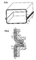
- FIG. 1 shows the perspective view of a cuboid, two-part closed housing, consisting of a housing base 1 and a housing cover 2.
- the contact surfaces of the two housing parts 1, 2 are enlarged by flange-like construction of the housing walls.
- the entire inner surface of the two housing parts 1, 2, including the contact surface, is designed with a flexible printed circuit board 3, 4 over the entire surface.
- the flexible printed circuit board is connected to the housing parts 1, 2 over the whole area by gluing.
- the flexible printed circuit board 3, 4 is a practical means of guiding an electrical conductor around the entire surface of a device. It is particularly advantageous that the conductors can be easily applied to a carrier film 7 using conventional technology. However, it is also possible to dispense with a flexible printed circuit board 3 and to apply the conductors directly in the housing walls or on the inner surface of the housing.
- FIG. 1 The area around the contact surfaces between the housing parts 1, 2 is shown enlarged in FIG.
- the flexible printed circuit boards 3, 4 glued onto each housing part 1, 2 and one contact point 13 each are shown.
- An adhesive layer 5 can be seen directly on the inner surface of the housing.
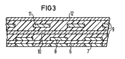
- This is followed by a shield layer 6, which consists of crossed conductors and is connected to the device ground.
- a carrier film 7 adjoins this screen layer 6.
- a first conductor layer 8 and a second conductor layer 10 are applied to this carrier film 7.
- the two conductor layers 8, 10 are electrically separated from one another by an insulating layer 9.
- the contact points 13 can be seen in the area of the contact surfaces between the housing parts 1, 2. These contact points 13 connect the conductors of the flexible printed circuit board 3 and the conductors of the flexible printed circuit board 4 to one another.
- the number of contact areas 13 is e.g. determined by the number of conductors in the flexible circuit boards 3, 4. If, for example, only one conductor is provided for each flexible printed circuit board 3, 4, which is looped through all existing conductor layers 8, 10, then in principle only one contact point 13 is required. However, if several conductors are routed in parallel per conductor layer 8, 10, or one or more conductors are assigned to individual or groups of individual conductor layers 8, 10, the number of contact points 13 required increases. With lower safety requirements, contact points 13 can be dispensed with entirely. In this case, each housing part 1, 2 is assigned at least one conductor which is separate from the other housing parts.
- the number of contact points 13 can be increased consciously.
- the conductors are then ground several times from one circuit board 3 to the other circuit board 4 and vice versa. If the contact points 13 are distributed at any spacing from one another over the entire contact surfaces, then there is a circumferential opening protection; ie at least one contact between the conductors of the printed circuit boards 3, 4 is always interrupted, regardless of which Place a scammer tries to get into the housing 1, 2 by prying open the contact surfaces.
- the shield layer 6 is applied to one side of the carrier film 7.
- the conductors of the first conductor layer 8 running in a meandering shape with a vertical preferred direction in the plane of the table can be seen.
- the conductors of all conductor layers 8, 10, 11, 12 have, for example, a width of 0.3 mm and a distance of 0.3 mm from one another.
- the first conductor layer 8 is covered by the insulating layer 9.
- the conductors of the second conductor layer 10 run in a meandering shape and with a preferred direction parallel to the plane of the board.
- a further insulating layer 9 is followed by a third conductor layer 11, in which the conductors, which also run in a meandering pattern, run into the plane of the panel as in the first conductor layer 8.
- the offset arrangement of the conductors of the third conductor layer 11 to the conductors of the first conductor layer 8 can be seen, since the conductors in the different conductor layers 8, 10, 11, 12 have the same width and the conductor width is approximately the distance between the conductors within a conductor layer 8, 10, 11, 12, it is easy to arrange the conductors in the third conductor layer 11 exactly above the locations of the first conductor layer 8 where the conductor-free areas are located there. This principle is also implemented in the even number of conductor layers 10, 12.
- the conductors of a fourth conductor layer 12, like the conductors of the second conductor layer 10, run parallel to the board level but offset by a conductor width from the conductors there.
- the protection against unauthorized access to the device electrical conductors are thus in four layers one above the other meandering and differently oriented so that penetration of the flexible circuit board 3, 4 without damaging at least one conductor seems completely impossible.
- the conductor layer 6 with crossed conductors on the other side of the carrier film 7 serves on the one hand to shield the device against electromagnetic interference.
- the grid structure, the individual conductors of which are congruent with the conductor of at least one of the other conductor layers 8, 10, 11, 12, additionally prevents the conductor routing of these conductor layers 8, 10, 11, 12 from being spied out.
- a special design of the conductor material opens up a further possibility of increasing security.
- a conductor material with a defined specific resistance for example a conductive varnish - any change in resistance in the conductor, for example due to conductor damage or bridging, can be detected when using an appropriately equipped evaluation circuit.
- Such an evaluation circuit is, for example, part of a flat module arranged in the device housing 1, 2.
- This printed circuit board is e.g. Electrically connected to the conductors of the flexible printed circuit board 3, 4 via loosely inserted contact elements.
- opening or deforming the housing also virtually leads to an interruption in the electrical conductor.
- the evaluation circuit receives only one protection criterion.
- Further Protection criteria are the supply voltage of the safety-relevant circuit parts of the device, the temperature of the housing and the temperature of the safety-relevant circuit parts.
- the safety-relevant circuit parts are, for example, a semiconductor data memory and the evaluation circuit itself.
- Electronic circuits are only functional in certain voltage and temperature ranges, which results in the possibility of manipulation at certain voltages and temperatures. Before such impermissible voltages, temperatures and when the electrical conductors are cut or damaged, the evaluation circuit destroys safety-relevant circuit parts and / or changes or deletes safety-relevant data.
- the evaluation circuit counteracts this effect by reversing the polarity of the supply voltage at the semiconductor memory in the event of non-compliance with the specified conditions. If this polarity reversal is intended to prevent the semiconductor memory from being destroyed, this can be achieved by a protective resistor in the supply voltage lines of the memory.
Landscapes
- Engineering & Computer Science (AREA)
- Computer Security & Cryptography (AREA)
- Computer Hardware Design (AREA)
- Theoretical Computer Science (AREA)
- Microelectronics & Electronic Packaging (AREA)
- Software Systems (AREA)
- Physics & Mathematics (AREA)
- General Engineering & Computer Science (AREA)
- General Physics & Mathematics (AREA)
- Storage Device Security (AREA)
- Structure Of Printed Boards (AREA)
- Signal Processing Not Specific To The Method Of Recording And Reproducing (AREA)
Applications Claiming Priority (2)
| Application Number | Priority Date | Filing Date | Title |
|---|---|---|---|
| DE4115703 | 1991-05-14 | ||
| DE4115703A DE4115703C1 (enExample) | 1991-05-14 | 1991-05-14 |
Publications (2)
| Publication Number | Publication Date |
|---|---|
| EP0514708A1 EP0514708A1 (de) | 1992-11-25 |
| EP0514708B1 true EP0514708B1 (de) | 1996-09-18 |
Family
ID=6431630
Family Applications (1)
| Application Number | Title | Priority Date | Filing Date |
|---|---|---|---|
| EP92107660A Expired - Lifetime EP0514708B1 (de) | 1991-05-14 | 1992-05-06 | Schutzvorrichtung für Schaltungsteile und/oder Daten in einem elektrotechnischen Gerät |
Country Status (4)
| Country | Link |
|---|---|
| EP (1) | EP0514708B1 (enExample) |
| AT (1) | ATE143210T1 (enExample) |
| DE (2) | DE4115703C1 (enExample) |
| ES (1) | ES2091358T3 (enExample) |
Cited By (1)
| Publication number | Priority date | Publication date | Assignee | Title |
|---|---|---|---|---|
| GB2444968A (en) * | 2006-12-22 | 2008-06-25 | Elmdene Internat Ltd | Alarm housing with cover opening tamper switch and cover penetration conductive grid sensor |
Families Citing this family (18)
| Publication number | Priority date | Publication date | Assignee | Title |
|---|---|---|---|---|
| DE4307208C1 (de) * | 1993-03-08 | 1994-05-19 | Ibm | Gehäuse |
| DE4312905C2 (de) * | 1993-04-16 | 1995-04-13 | Krone Ag | Schutzeinrichtung zur Sicherung von gespeicherten Daten |
| EP0622719B1 (de) * | 1993-04-28 | 2001-11-14 | Fujitsu Siemens Computers GmbH | Schutzvorrichtung für Schaltungsteile und/oder Daten eines elektrotechnischen Geräts |
| DE4415200C1 (de) * | 1994-04-30 | 1995-08-03 | Gundokar Braumann | Packelement und Vorrichtung mit diesem Element |
| DE4447631C2 (de) * | 1994-04-30 | 1998-09-24 | Gundokar Braumann | Packelement, Vorrichtung mit diesem Packelement und Verfahren zum Aufbringen einer Leiterbahn auf ein Packelement |
| DE19512266C2 (de) * | 1994-09-23 | 1998-11-19 | Rainer Jacob | Diebstahlschutzsystem für Fahrzeuge |
| DE19536477C2 (de) * | 1995-09-29 | 1997-10-23 | Siemens Nixdorf Inf Syst | Schaltungsanordnung zur Sicherung elektronischer Bauteile |
| DE19612167A1 (de) * | 1996-03-27 | 1997-10-02 | Gundokar Braumann | Gehäuse und Verfahren zum Herstellen des Gehäuses |
| GB2315586B (en) * | 1996-07-19 | 2000-08-30 | Neopost Ltd | Apparatus with tamper detector |
| DE19707437A1 (de) * | 1997-02-25 | 1998-08-27 | Michael Albert Volz | Verfahren zur Herstellung eines mehrteiligen Gehäuses für die dem Funkempfänger einer Fernsteuereinrichtung zugeordnete Rudermaschine eines Fahrzeugmodells sowie das Gehäuse der Rudermaschine selbst |
| DE29722653U1 (de) * | 1997-12-22 | 1999-01-28 | Siemens Ag | Manipulationsgeschütztes elektrisches Gerät |
| DE19904979A1 (de) * | 1999-02-06 | 2000-08-10 | Valeo Schalter & Sensoren Gmbh | Leiterplatte für einen elektrischen Schalter |
| AU2001239854A1 (en) * | 2000-02-23 | 2001-09-03 | Iridian Technologies, Inc. | Tamper proof case for electronic devices having memories with sensitive information |
| GB2363233B (en) | 2000-05-11 | 2004-03-31 | Ibm | Tamper resistant card enclosure with improved intrusion detection circuit |
| DE10047436A1 (de) * | 2000-09-21 | 2002-08-29 | Giesecke & Devrient Gmbh | Sicherheitsmodul |
| US7323986B2 (en) * | 2004-09-03 | 2008-01-29 | Gore Enterprise Holdings, Inc. | Reusable tamper respondent enclosure |
| DE102007061254B4 (de) * | 2007-06-12 | 2009-08-27 | Hypercom Gmbh | Mehrteiliges Gehäuse für eine Sicherungsvorrichtung |
| DE102015122000B4 (de) * | 2015-12-16 | 2019-02-07 | Fujitsu Client Computing Limited | Anordnung und elektronisches Gerät |
Family Cites Families (7)
| Publication number | Priority date | Publication date | Assignee | Title |
|---|---|---|---|---|
| CH640971A5 (en) * | 1979-06-28 | 1984-01-31 | Kurt Ehrat | Mobile data container secured against unauthorised access |
| DE3347483A1 (de) * | 1983-12-29 | 1985-07-11 | GAO Gesellschaft für Automation und Organisation mbH, 8000 München | Vorrichtung zur sicherung geheimer informationen |
| DE3602960C1 (de) * | 1986-01-31 | 1987-02-19 | Philips Patentverwaltung | Dickschicht-Schaltungsanordnung mit einer keramischen Substratplatte |
| DE3624718A1 (de) * | 1986-07-22 | 1988-01-28 | Schoeller & Co Elektronik | Mehrlagige, starre und flexible bereiche aufweisende leiterplatte |
| DE3627105A1 (de) * | 1986-08-06 | 1988-02-11 | Svenska Arkivator Ab | Sicherheitsbehaelter |
| CA1294117C (en) * | 1986-09-29 | 1992-01-14 | S. Eugene Benge | Method of making deactivatable tags |
| US4846922A (en) * | 1986-09-29 | 1989-07-11 | Monarch Marking Systems, Inc. | Method of making deactivatable tags |
-
1991
- 1991-05-14 DE DE4115703A patent/DE4115703C1/de not_active Expired - Lifetime
-
1992
- 1992-05-06 DE DE59207156T patent/DE59207156D1/de not_active Expired - Fee Related
- 1992-05-06 EP EP92107660A patent/EP0514708B1/de not_active Expired - Lifetime
- 1992-05-06 ES ES92107660T patent/ES2091358T3/es not_active Expired - Lifetime
- 1992-05-06 AT AT92107660T patent/ATE143210T1/de not_active IP Right Cessation
Cited By (2)
| Publication number | Priority date | Publication date | Assignee | Title |
|---|---|---|---|---|
| GB2444968A (en) * | 2006-12-22 | 2008-06-25 | Elmdene Internat Ltd | Alarm housing with cover opening tamper switch and cover penetration conductive grid sensor |
| GB2444968B (en) * | 2006-12-22 | 2011-06-22 | Elmdene Internat Ltd | Alarm unit |
Also Published As
| Publication number | Publication date |
|---|---|
| ATE143210T1 (de) | 1996-10-15 |
| DE59207156D1 (de) | 1996-10-24 |
| DE4115703C1 (enExample) | 1992-08-27 |
| ES2091358T3 (es) | 1996-11-01 |
| EP0514708A1 (de) | 1992-11-25 |
Similar Documents
| Publication | Publication Date | Title |
|---|---|---|
| EP0514708B1 (de) | Schutzvorrichtung für Schaltungsteile und/oder Daten in einem elektrotechnischen Gerät | |
| DE3635938C2 (enExample) | ||
| DE3730554C2 (de) | Sicherheitseinrichtung zum schützen gespeicherter sensitiver daten | |
| DE69314742T2 (de) | Vorrichtung zum Schutz gegen elektrische Überbeanspruchung | |
| DE3632144C2 (enExample) | ||
| DE60130154T2 (de) | Ein kartenlesegerät | |
| EP1924947B1 (de) | Manipulations- und durchbohrschutz für eine an eine elektrische schaltung anzuschliessende vorrichtung | |
| EP0785708A1 (de) | Anordnung zum Schutz elektrischer und elektronischer Bauelmente vor elektrostatischen Entladungen | |
| DE4312905C2 (de) | Schutzeinrichtung zur Sicherung von gespeicherten Daten | |
| DE19600770A1 (de) | Sicherheitsfolie mit EMV-Schutz | |
| DE19600769A1 (de) | Sicherheitsmodul mit einteiliger Sicherheitsfolie | |
| DE9105960U1 (de) | Schutzvorrichtung für Schaltungsteile und/oder Daten in einem Gerät zur Authentifikation und Betragsbestätigung | |
| DE19717032C2 (de) | Elektronische Baugruppe mit Mitteln zum Verhindern von Feuchtigkeitseinflüssen | |
| DE69223073T2 (de) | Datensicherheitsvorrichtung | |
| DE10337567B3 (de) | Schutzstruktur für Hardware mit hochauflösenden Elastomeren | |
| EP0622719B1 (de) | Schutzvorrichtung für Schaltungsteile und/oder Daten eines elektrotechnischen Geräts | |
| DE10340289A1 (de) | Sicherungseinrichtung für Hardwarebaugruppen | |
| EP1323015A1 (de) | Sicherheitsmodul | |
| DE10140045B4 (de) | IC-Chip mit Schutzstruktur | |
| WO2001037230A1 (de) | Elektronisches bauelement und verfahren zum schützen einer in dem bauelement enthaltenen integrierten schaltung | |
| DE10065339B4 (de) | Kapazitiver Sensor als Schutzvorrichtung gegen Angriffe auf einen Sicherheitschip | |
| EP1058178B1 (de) | Schutzschaltung | |
| EP1746872B1 (de) | Leiterplattenanordnung und Verfahren zu deren Herstellung | |
| DE60201507T2 (de) | Eindringgeschütztes Gehäuse mit Widerstandsmaschennetzwerk | |
| EP3478032B1 (de) | Leiterplatte und verwendung einer kantenschutzleiste |
Legal Events
| Date | Code | Title | Description |
|---|---|---|---|
| PUAI | Public reference made under article 153(3) epc to a published international application that has entered the european phase |
Free format text: ORIGINAL CODE: 0009012 |
|
| AK | Designated contracting states |
Kind code of ref document: A1 Designated state(s): AT BE CH DE ES FR GB IT LI NL SE |
|
| 17P | Request for examination filed |
Effective date: 19921208 |
|
| GRAG | Despatch of communication of intention to grant |
Free format text: ORIGINAL CODE: EPIDOS AGRA |
|
| GRAH | Despatch of communication of intention to grant a patent |
Free format text: ORIGINAL CODE: EPIDOS IGRA |
|
| 17Q | First examination report despatched |
Effective date: 19960227 |
|
| GRAH | Despatch of communication of intention to grant a patent |
Free format text: ORIGINAL CODE: EPIDOS IGRA |
|
| GRAA | (expected) grant |
Free format text: ORIGINAL CODE: 0009210 |
|
| AK | Designated contracting states |
Kind code of ref document: B1 Designated state(s): AT BE CH DE ES FR GB IT LI NL SE |
|
| REF | Corresponds to: |
Ref document number: 143210 Country of ref document: AT Date of ref document: 19961015 Kind code of ref document: T |
|
| REG | Reference to a national code |
Ref country code: CH Ref legal event code: NV Representative=s name: SIEMENS SCHWEIZ AG |
|
| REF | Corresponds to: |
Ref document number: 59207156 Country of ref document: DE Date of ref document: 19961024 |
|
| REG | Reference to a national code |
Ref country code: ES Ref legal event code: FG2A Ref document number: 2091358 Country of ref document: ES Kind code of ref document: T3 |
|
| ET | Fr: translation filed | ||
| ITF | It: translation for a ep patent filed | ||
| GBT | Gb: translation of ep patent filed (gb section 77(6)(a)/1977) |
Effective date: 19961122 |
|
| PLBE | No opposition filed within time limit |
Free format text: ORIGINAL CODE: 0009261 |
|
| STAA | Information on the status of an ep patent application or granted ep patent |
Free format text: STATUS: NO OPPOSITION FILED WITHIN TIME LIMIT |
|
| 26N | No opposition filed | ||
| PG25 | Lapsed in a contracting state [announced via postgrant information from national office to epo] |
Ref country code: DE Free format text: LAPSE BECAUSE OF NON-PAYMENT OF DUE FEES Effective date: 19980203 |
|
| REG | Reference to a national code |
Ref country code: CH Ref legal event code: PUE Owner name: SIEMENS NIXDORF INFORMATIONSSYSTEME AKTIENGESELLSC |
|
| REG | Reference to a national code |
Ref country code: CH Ref legal event code: NV Representative=s name: E. BLUM & CO. PATENTANWAELTE |
|
| REG | Reference to a national code |
Ref country code: FR Ref legal event code: TP |
|
| REG | Reference to a national code |
Ref country code: GB Ref legal event code: 732E |
|
| BECA | Be: change of holder's address |
Free format text: 20010405 *FUJITSU SIEMENS COMPUTERS G.M.B.H.:OTTO-HAHN-RING 6, 81739 MUENCHEN |
|
| REG | Reference to a national code |
Ref country code: GB Ref legal event code: IF02 |
|
| PGFP | Annual fee paid to national office [announced via postgrant information from national office to epo] |
Ref country code: NL Payment date: 20040416 Year of fee payment: 13 |
|
| PGFP | Annual fee paid to national office [announced via postgrant information from national office to epo] |
Ref country code: AT Payment date: 20040421 Year of fee payment: 13 |
|
| PGFP | Annual fee paid to national office [announced via postgrant information from national office to epo] |
Ref country code: GB Payment date: 20040428 Year of fee payment: 13 |
|
| PGFP | Annual fee paid to national office [announced via postgrant information from national office to epo] |
Ref country code: FR Payment date: 20040519 Year of fee payment: 13 |
|
| PGFP | Annual fee paid to national office [announced via postgrant information from national office to epo] |
Ref country code: SE Payment date: 20040521 Year of fee payment: 13 |
|
| PGFP | Annual fee paid to national office [announced via postgrant information from national office to epo] |
Ref country code: CH Payment date: 20040524 Year of fee payment: 13 |
|
| PGFP | Annual fee paid to national office [announced via postgrant information from national office to epo] |
Ref country code: ES Payment date: 20040609 Year of fee payment: 13 |
|
| PGFP | Annual fee paid to national office [announced via postgrant information from national office to epo] |
Ref country code: BE Payment date: 20040622 Year of fee payment: 13 |
|
| PG25 | Lapsed in a contracting state [announced via postgrant information from national office to epo] |
Ref country code: IT Free format text: LAPSE BECAUSE OF NON-PAYMENT OF DUE FEES;WARNING: LAPSES OF ITALIAN PATENTS WITH EFFECTIVE DATE BEFORE 2007 MAY HAVE OCCURRED AT ANY TIME BEFORE 2007. THE CORRECT EFFECTIVE DATE MAY BE DIFFERENT FROM THE ONE RECORDED. Effective date: 20050506 Ref country code: GB Free format text: LAPSE BECAUSE OF NON-PAYMENT OF DUE FEES Effective date: 20050506 Ref country code: AT Free format text: LAPSE BECAUSE OF NON-PAYMENT OF DUE FEES Effective date: 20050506 |
|
| PG25 | Lapsed in a contracting state [announced via postgrant information from national office to epo] |
Ref country code: SE Free format text: LAPSE BECAUSE OF NON-PAYMENT OF DUE FEES Effective date: 20050507 Ref country code: ES Free format text: LAPSE BECAUSE OF NON-PAYMENT OF DUE FEES Effective date: 20050507 |
|
| PG25 | Lapsed in a contracting state [announced via postgrant information from national office to epo] |
Ref country code: LI Free format text: LAPSE BECAUSE OF NON-PAYMENT OF DUE FEES Effective date: 20050531 Ref country code: CH Free format text: LAPSE BECAUSE OF NON-PAYMENT OF DUE FEES Effective date: 20050531 Ref country code: BE Free format text: LAPSE BECAUSE OF NON-PAYMENT OF DUE FEES Effective date: 20050531 |
|
| BERE | Be: lapsed |
Owner name: *FUJITSU SIEMENS COMPUTERS G.M.B.H. Effective date: 20050531 |
|
| PG25 | Lapsed in a contracting state [announced via postgrant information from national office to epo] |
Ref country code: NL Free format text: LAPSE BECAUSE OF NON-PAYMENT OF DUE FEES Effective date: 20051201 |
|
| REG | Reference to a national code |
Ref country code: CH Ref legal event code: PL |
|
| EUG | Se: european patent has lapsed | ||
| GBPC | Gb: european patent ceased through non-payment of renewal fee |
Effective date: 20050506 |
|
| PG25 | Lapsed in a contracting state [announced via postgrant information from national office to epo] |
Ref country code: FR Free format text: LAPSE BECAUSE OF NON-PAYMENT OF DUE FEES Effective date: 20060131 |
|
| NLV4 | Nl: lapsed or anulled due to non-payment of the annual fee |
Effective date: 20051201 |
|
| REG | Reference to a national code |
Ref country code: FR Ref legal event code: ST Effective date: 20060131 |
|
| REG | Reference to a national code |
Ref country code: ES Ref legal event code: FD2A Effective date: 20050507 |
|
| BERE | Be: lapsed |
Owner name: *FUJITSU SIEMENS COMPUTERS G.M.B.H. Effective date: 20050531 |