EP0509907A1 - CVD-Verfahren zum Herstellen einer Siliziumdiffusionsschicht und/oder Überzug auf der Oberfläche eines Metallsubstrates - Google Patents
CVD-Verfahren zum Herstellen einer Siliziumdiffusionsschicht und/oder Überzug auf der Oberfläche eines Metallsubstrates Download PDFInfo
- Publication number
- EP0509907A1 EP0509907A1 EP92401046A EP92401046A EP0509907A1 EP 0509907 A1 EP0509907 A1 EP 0509907A1 EP 92401046 A EP92401046 A EP 92401046A EP 92401046 A EP92401046 A EP 92401046A EP 0509907 A1 EP0509907 A1 EP 0509907A1
- Authority
- EP
- European Patent Office
- Prior art keywords
- silicon
- sample
- diffusion
- enclosure
- temperature
- Prior art date
- Legal status (The legal status is an assumption and is not a legal conclusion. Google has not performed a legal analysis and makes no representation as to the accuracy of the status listed.)
- Granted
Links
- 238000000576 coating method Methods 0.000 title claims abstract description 84
- 229910052710 silicon Inorganic materials 0.000 title claims abstract description 79
- 238000009792 diffusion process Methods 0.000 title claims abstract description 75
- 239000010703 silicon Substances 0.000 title claims abstract description 69
- XUIMIQQOPSSXEZ-UHFFFAOYSA-N Silicon Chemical compound [Si] XUIMIQQOPSSXEZ-UHFFFAOYSA-N 0.000 title claims abstract description 68
- 239000000758 substrate Substances 0.000 title claims abstract description 38
- 239000011248 coating agent Substances 0.000 title claims abstract description 35
- 238000000034 method Methods 0.000 title claims abstract description 32
- 238000005229 chemical vapour deposition Methods 0.000 title description 37
- BLRPTPMANUNPDV-UHFFFAOYSA-N Silane Chemical compound [SiH4] BLRPTPMANUNPDV-UHFFFAOYSA-N 0.000 claims abstract description 49
- 239000000203 mixture Substances 0.000 claims abstract description 20
- 238000000151 deposition Methods 0.000 claims abstract description 13
- 230000008021 deposition Effects 0.000 claims abstract description 13
- 238000004518 low pressure chemical vapour deposition Methods 0.000 claims abstract description 12
- 238000010438 heat treatment Methods 0.000 claims abstract description 7
- 229910052990 silicon hydride Inorganic materials 0.000 claims abstract description 5
- 238000001816 cooling Methods 0.000 claims abstract 2
- XEEYBQQBJWHFJM-UHFFFAOYSA-N Iron Chemical compound [Fe] XEEYBQQBJWHFJM-UHFFFAOYSA-N 0.000 claims description 36
- 229910052742 iron Inorganic materials 0.000 claims description 19
- 238000005498 polishing Methods 0.000 claims description 11
- 238000004140 cleaning Methods 0.000 claims description 10
- 238000010943 off-gassing Methods 0.000 claims description 8
- 239000000956 alloy Substances 0.000 claims description 7
- 238000001179 sorption measurement Methods 0.000 claims description 7
- 239000000126 substance Substances 0.000 claims description 6
- 229910045601 alloy Inorganic materials 0.000 claims description 5
- 229910052751 metal Inorganic materials 0.000 claims description 4
- 239000002184 metal Substances 0.000 claims description 4
- 239000011247 coating layer Substances 0.000 claims description 2
- 229910052782 aluminium Inorganic materials 0.000 claims 1
- 229910052802 copper Inorganic materials 0.000 claims 1
- 229910052749 magnesium Inorganic materials 0.000 claims 1
- 229910052748 manganese Inorganic materials 0.000 claims 1
- 229910052750 molybdenum Inorganic materials 0.000 claims 1
- 229910052759 nickel Inorganic materials 0.000 claims 1
- 229910052758 niobium Inorganic materials 0.000 claims 1
- 229910052761 rare earth metal Inorganic materials 0.000 claims 1
- 150000002910 rare earth metals Chemical class 0.000 claims 1
- 229910052715 tantalum Inorganic materials 0.000 claims 1
- 229910052719 titanium Inorganic materials 0.000 claims 1
- 229910052721 tungsten Inorganic materials 0.000 claims 1
- 229910052720 vanadium Inorganic materials 0.000 claims 1
- 229910052726 zirconium Inorganic materials 0.000 claims 1
- 239000002904 solvent Substances 0.000 abstract description 3
- 239000007789 gas Substances 0.000 description 37
- 239000010410 layer Substances 0.000 description 28
- 229910000077 silane Inorganic materials 0.000 description 19
- 238000005260 corrosion Methods 0.000 description 9
- 230000007797 corrosion Effects 0.000 description 9
- 230000000694 effects Effects 0.000 description 9
- XKRFYHLGVUSROY-UHFFFAOYSA-N Argon Chemical compound [Ar] XKRFYHLGVUSROY-UHFFFAOYSA-N 0.000 description 8
- 229910052786 argon Inorganic materials 0.000 description 7
- 229910052734 helium Inorganic materials 0.000 description 7
- UFHFLCQGNIYNRP-UHFFFAOYSA-N Hydrogen Chemical compound [H][H] UFHFLCQGNIYNRP-UHFFFAOYSA-N 0.000 description 6
- 230000015572 biosynthetic process Effects 0.000 description 6
- 239000001257 hydrogen Substances 0.000 description 6
- 229910052739 hydrogen Inorganic materials 0.000 description 6
- 239000000463 material Substances 0.000 description 6
- 239000011261 inert gas Substances 0.000 description 5
- CSCPPACGZOOCGX-UHFFFAOYSA-N Acetone Chemical compound CC(C)=O CSCPPACGZOOCGX-UHFFFAOYSA-N 0.000 description 4
- 238000002474 experimental method Methods 0.000 description 4
- 239000001307 helium Substances 0.000 description 4
- SWQJXJOGLNCZEY-UHFFFAOYSA-N helium atom Chemical compound [He] SWQJXJOGLNCZEY-UHFFFAOYSA-N 0.000 description 4
- 238000004519 manufacturing process Methods 0.000 description 4
- FDNAPBUWERUEDA-UHFFFAOYSA-N silicon tetrachloride Chemical compound Cl[Si](Cl)(Cl)Cl FDNAPBUWERUEDA-UHFFFAOYSA-N 0.000 description 4
- 239000006104 solid solution Substances 0.000 description 4
- 229910001220 stainless steel Inorganic materials 0.000 description 4
- 229910003910 SiCl4 Inorganic materials 0.000 description 3
- VYPSYNLAJGMNEJ-UHFFFAOYSA-N Silicium dioxide Chemical compound O=[Si]=O VYPSYNLAJGMNEJ-UHFFFAOYSA-N 0.000 description 3
- 229910052799 carbon Inorganic materials 0.000 description 3
- 230000007423 decrease Effects 0.000 description 3
- 238000009826 distribution Methods 0.000 description 3
- 238000002347 injection Methods 0.000 description 3
- 239000007924 injection Substances 0.000 description 3
- 239000010935 stainless steel Substances 0.000 description 3
- 238000004506 ultrasonic cleaning Methods 0.000 description 3
- 229910000640 Fe alloy Inorganic materials 0.000 description 2
- 229910017384 Fe3Si Inorganic materials 0.000 description 2
- 229910015364 Fe5Si3 Inorganic materials 0.000 description 2
- 229910000676 Si alloy Inorganic materials 0.000 description 2
- PNEYBMLMFCGWSK-UHFFFAOYSA-N aluminium oxide Inorganic materials [O-2].[O-2].[O-2].[Al+3].[Al+3] PNEYBMLMFCGWSK-UHFFFAOYSA-N 0.000 description 2
- QVGXLLKOCUKJST-UHFFFAOYSA-N atomic oxygen Chemical compound [O] QVGXLLKOCUKJST-UHFFFAOYSA-N 0.000 description 2
- 238000007865 diluting Methods 0.000 description 2
- 239000012895 dilution Substances 0.000 description 2
- 238000010790 dilution Methods 0.000 description 2
- XWHPIFXRKKHEKR-UHFFFAOYSA-N iron silicon Chemical compound [Si].[Fe] XWHPIFXRKKHEKR-UHFFFAOYSA-N 0.000 description 2
- 150000002739 metals Chemical class 0.000 description 2
- 230000003647 oxidation Effects 0.000 description 2
- 238000007254 oxidation reaction Methods 0.000 description 2
- 239000001301 oxygen Substances 0.000 description 2
- 229910052760 oxygen Inorganic materials 0.000 description 2
- 239000000843 powder Substances 0.000 description 2
- 238000002360 preparation method Methods 0.000 description 2
- 238000005086 pumping Methods 0.000 description 2
- 230000002787 reinforcement Effects 0.000 description 2
- 238000004381 surface treatment Methods 0.000 description 2
- 229910000851 Alloy steel Inorganic materials 0.000 description 1
- ZAMOUSCENKQFHK-UHFFFAOYSA-N Chlorine atom Chemical compound [Cl] ZAMOUSCENKQFHK-UHFFFAOYSA-N 0.000 description 1
- 229910000976 Electrical steel Inorganic materials 0.000 description 1
- 229910017082 Fe-Si Inorganic materials 0.000 description 1
- 229910005347 FeSi Inorganic materials 0.000 description 1
- 229910005331 FeSi2 Inorganic materials 0.000 description 1
- 229910017133 Fe—Si Inorganic materials 0.000 description 1
- 229910021577 Iron(II) chloride Inorganic materials 0.000 description 1
- 229910052581 Si3N4 Inorganic materials 0.000 description 1
- 229910000831 Steel Inorganic materials 0.000 description 1
- 238000002441 X-ray diffraction Methods 0.000 description 1
- 238000005299 abrasion Methods 0.000 description 1
- 238000010521 absorption reaction Methods 0.000 description 1
- 239000002253 acid Substances 0.000 description 1
- 239000003929 acidic solution Substances 0.000 description 1
- 150000007513 acids Chemical class 0.000 description 1
- 238000004458 analytical method Methods 0.000 description 1
- 238000001505 atmospheric-pressure chemical vapour deposition Methods 0.000 description 1
- 239000012159 carrier gas Substances 0.000 description 1
- 238000003486 chemical etching Methods 0.000 description 1
- 238000006243 chemical reaction Methods 0.000 description 1
- 239000000460 chlorine Substances 0.000 description 1
- 229910052801 chlorine Inorganic materials 0.000 description 1
- 229910052681 coesite Inorganic materials 0.000 description 1
- 150000001875 compounds Chemical class 0.000 description 1
- 238000010276 construction Methods 0.000 description 1
- 238000004320 controlled atmosphere Methods 0.000 description 1
- 229910052593 corundum Inorganic materials 0.000 description 1
- 229910052906 cristobalite Inorganic materials 0.000 description 1
- 239000013078 crystal Substances 0.000 description 1
- 230000003247 decreasing effect Effects 0.000 description 1
- 230000006866 deterioration Effects 0.000 description 1
- 229910003460 diamond Inorganic materials 0.000 description 1
- 239000010432 diamond Substances 0.000 description 1
- 238000000921 elemental analysis Methods 0.000 description 1
- 238000005516 engineering process Methods 0.000 description 1
- 238000005530 etching Methods 0.000 description 1
- 150000004678 hydrides Chemical class 0.000 description 1
- 150000002431 hydrogen Chemical class 0.000 description 1
- 239000012535 impurity Substances 0.000 description 1
- 238000011065 in-situ storage Methods 0.000 description 1
- NMCUIPGRVMDVDB-UHFFFAOYSA-L iron dichloride Chemical compound Cl[Fe]Cl NMCUIPGRVMDVDB-UHFFFAOYSA-L 0.000 description 1
- 230000000877 morphologic effect Effects 0.000 description 1
- 230000006911 nucleation Effects 0.000 description 1
- 238000010899 nucleation Methods 0.000 description 1
- 239000003960 organic solvent Substances 0.000 description 1
- 230000001590 oxidative effect Effects 0.000 description 1
- 230000035484 reaction time Effects 0.000 description 1
- 238000000682 scanning probe acoustic microscopy Methods 0.000 description 1
- 229910021332 silicide Inorganic materials 0.000 description 1
- 150000003377 silicon compounds Chemical class 0.000 description 1
- 239000000377 silicon dioxide Substances 0.000 description 1
- 235000012239 silicon dioxide Nutrition 0.000 description 1
- HQVNEWCFYHHQES-UHFFFAOYSA-N silicon nitride Chemical compound N12[Si]34N5[Si]62N3[Si]51N64 HQVNEWCFYHHQES-UHFFFAOYSA-N 0.000 description 1
- 229910052814 silicon oxide Inorganic materials 0.000 description 1
- 239000011856 silicon-based particle Substances 0.000 description 1
- 239000010959 steel Substances 0.000 description 1
- 229910052682 stishovite Inorganic materials 0.000 description 1
- 238000000859 sublimation Methods 0.000 description 1
- 230000008022 sublimation Effects 0.000 description 1
- 239000002344 surface layer Substances 0.000 description 1
- 238000007669 thermal treatment Methods 0.000 description 1
- 229910052905 tridymite Inorganic materials 0.000 description 1
- 230000004580 weight loss Effects 0.000 description 1
- 229910001845 yogo sapphire Inorganic materials 0.000 description 1
Images




Classifications
-
- C—CHEMISTRY; METALLURGY
- C23—COATING METALLIC MATERIAL; COATING MATERIAL WITH METALLIC MATERIAL; CHEMICAL SURFACE TREATMENT; DIFFUSION TREATMENT OF METALLIC MATERIAL; COATING BY VACUUM EVAPORATION, BY SPUTTERING, BY ION IMPLANTATION OR BY CHEMICAL VAPOUR DEPOSITION, IN GENERAL; INHIBITING CORROSION OF METALLIC MATERIAL OR INCRUSTATION IN GENERAL
- C23C—COATING METALLIC MATERIAL; COATING MATERIAL WITH METALLIC MATERIAL; SURFACE TREATMENT OF METALLIC MATERIAL BY DIFFUSION INTO THE SURFACE, BY CHEMICAL CONVERSION OR SUBSTITUTION; COATING BY VACUUM EVAPORATION, BY SPUTTERING, BY ION IMPLANTATION OR BY CHEMICAL VAPOUR DEPOSITION, IN GENERAL
- C23C16/00—Chemical coating by decomposition of gaseous compounds, without leaving reaction products of surface material in the coating, i.e. chemical vapour deposition [CVD] processes
- C23C16/22—Chemical coating by decomposition of gaseous compounds, without leaving reaction products of surface material in the coating, i.e. chemical vapour deposition [CVD] processes characterised by the deposition of inorganic material, other than metallic material
- C23C16/24—Deposition of silicon only
-
- C—CHEMISTRY; METALLURGY
- C23—COATING METALLIC MATERIAL; COATING MATERIAL WITH METALLIC MATERIAL; CHEMICAL SURFACE TREATMENT; DIFFUSION TREATMENT OF METALLIC MATERIAL; COATING BY VACUUM EVAPORATION, BY SPUTTERING, BY ION IMPLANTATION OR BY CHEMICAL VAPOUR DEPOSITION, IN GENERAL; INHIBITING CORROSION OF METALLIC MATERIAL OR INCRUSTATION IN GENERAL
- C23C—COATING METALLIC MATERIAL; COATING MATERIAL WITH METALLIC MATERIAL; SURFACE TREATMENT OF METALLIC MATERIAL BY DIFFUSION INTO THE SURFACE, BY CHEMICAL CONVERSION OR SUBSTITUTION; COATING BY VACUUM EVAPORATION, BY SPUTTERING, BY ION IMPLANTATION OR BY CHEMICAL VAPOUR DEPOSITION, IN GENERAL
- C23C10/00—Solid state diffusion of only metal elements or silicon into metallic material surfaces
- C23C10/06—Solid state diffusion of only metal elements or silicon into metallic material surfaces using gases
- C23C10/08—Solid state diffusion of only metal elements or silicon into metallic material surfaces using gases only one element being diffused
-
- C—CHEMISTRY; METALLURGY
- C23—COATING METALLIC MATERIAL; COATING MATERIAL WITH METALLIC MATERIAL; CHEMICAL SURFACE TREATMENT; DIFFUSION TREATMENT OF METALLIC MATERIAL; COATING BY VACUUM EVAPORATION, BY SPUTTERING, BY ION IMPLANTATION OR BY CHEMICAL VAPOUR DEPOSITION, IN GENERAL; INHIBITING CORROSION OF METALLIC MATERIAL OR INCRUSTATION IN GENERAL
- C23C—COATING METALLIC MATERIAL; COATING MATERIAL WITH METALLIC MATERIAL; SURFACE TREATMENT OF METALLIC MATERIAL BY DIFFUSION INTO THE SURFACE, BY CHEMICAL CONVERSION OR SUBSTITUTION; COATING BY VACUUM EVAPORATION, BY SPUTTERING, BY ION IMPLANTATION OR BY CHEMICAL VAPOUR DEPOSITION, IN GENERAL
- C23C16/00—Chemical coating by decomposition of gaseous compounds, without leaving reaction products of surface material in the coating, i.e. chemical vapour deposition [CVD] processes
- C23C16/02—Pretreatment of the material to be coated
- C23C16/0209—Pretreatment of the material to be coated by heating
Definitions
- the invention relates to the formation of a silicon diffusion and/or overlay coating on the surface of metallic substrate by Chemical Vapor Deposition (CVD) and more particularly on iron and iron-base alloys.
- CVD Chemical Vapor Deposition
- Silicon surface diffusion on iron-based metals i.e. iron and iron alloys and other metals as well, has been performed by Chemical vapor deposition from SiH4 and SiCl4 gases, under particular conditions disclosed hereunder. It is known from Japanese Patent Applications 62-227036, 62-227035 and 62-227033, all assigned to NKK to use silicon chloride SiCl4 with an atmospheric pressure CVD process to make silicon surface diffusion on iron and iron-silicon steel.
- the process disclosed in those three patent applications is similar and is consisting of a first step wherein the sample surface is cleaned with polishing means or chemical means, a second step consisting of an atmospheric pressure SiCl4 injection in the CVD enclosure under high temperature conditions between 1100 and 1250°C and a third step consisting of a diffusion of the silicon deposited during step 2 inside the sample at a temperature between 1200 and 1300°C under an atmosphere of inert or non-oxidizing gases.
- This process has drawbacks due essentially to the high temperature requirements and to the sample weight loss by sublimation of the in-situ generated FeCl2, which induces a certain porosity of the sample after treatment and to difficulties to handle the chlorine base corrosive gases at the exhaust of the CVD enclosure.
- USP 4 714 632 disclosed a method of forming a silicon diffusion coating on the surface of a metallic sample consisting of a first step wherein the sample is heated below 1200°C under a hydrogen atmosphere and a second step consisting of a heat treatment at atmospheric pressure at a temperature of less than 1000°C under a controlled atmosphere of a gas mixture consisting of silane, and hydrogen. Overlay coating was performed by further thermal treatment under an oxygen donor gas the balance being pure hydrogen.
- Cabrera et al in an article entitled "Formation of silicon diffusion coatings on ferrous alloys from their reaction with Silane", surface and Coating Technology, 39/40 (1989) - pages 43 to 51. However this process is limited to thin diffusion layers, i.e.
- pretreatment takes a long time (about 1h) while a large amount of hydrogen gas (about 1.51:min) is needed for both pretreatment and treatment steps. Diffusion coatings of FeSi x and overlayer coatings of SiO2 can be obtained with said process.
- the present invention provides a method of forming a silicon diffusion coating and/or a silicon base overlay coating on the surface of a metallic substrate, preferably an iron-base alloy.
- This method is carried out at reduced pressure in a cold wall Low Pressure Chemical Vapor Deposition (LPCVD) enclosure and at a temperature which can be as low as 50°C using pure silane or a gas mixture comprising silane and a gas selected from the group comprising Helium, Hydrogen, Argon or a mixture thereof.
- LPCVD cold wall Low Pressure Chemical Vapor Deposition
- the overlay coatings are always dominated by high concentrations of Si (>30 At.%) with concentration and thickness which might fluctuate considerably.
- the Si content of the overlay coatings generally increases with the layer thickness.
- the grain size of the overlay coatings varies from very fine (>0.5 ⁇ ) to about 20 Microns across, while the grains are generally, rounded, angular, elongated or platey with respect to the experimental conditions. Except at very high Si concentrations (>90 At.%), the grains of the overlay coatings are normally not attached to each other and the individual grain boundaries are distinct. However, the individual grains are indistinguishable when the Si content exceeds 90 At.%.
- XRD analysis reveals the presence of FeSi and Fe5Si3 phases in the overlay coatings. Weak peaks corresponding to FeSi2 have been also identified occasionally. The presence of silicon phase, which is not detected by XRD, is inferred from the high Si concentration of overlay coatings.
- the Si content is always less than 30 At.%, and the average layer growth rate is higher than that of the overlay coatings.
- the grains are usually large (>10 Microns), strongly attached to each other and occur in polygonal form (mainly hexagonal) in the case of diffusion coatings.
- the XRD peaks of the diffusion coatings with 2-4 At. % Si indicate solid-solution.
- the diffusion layers containing 26-29 At. % Si are almost entirely comprised Fe3Si phase, some times with small amounts of Fe5Si3, which is a high temperature phase.
- the temperature of the substrate affects strongly on coating characteristics. Both the Si concentration and growth rate of the coatings change with the temperature. The coatings are always overlay within 350-650°C as demonstrated by the high Si concentration (>30 At. %) and the morphological characteristics. When the temperature exceeds 650°C, diffusion layers with variable Si content (always ⁇ 29 At.%) depending on the gas flow rate occurs.
- the surface morphology of the coatings show,gradual variation from 350 to 650°C and then change dramatically with increasing temperature.
- the grain size generally increases and the grain shape changes from rounded or angular to elongated or platey form with the increase of temperature from 350°C-650°C.
- most of the grains are not bonded together and seem to possess distinct margins at low temperatures, but individual grain margins gradually disappear and become replaced by common boundaries with increasing temperature.
- the grain size sharply increases and the shape changes to polygonal (mainly hexagonal).
- the Si content of the depositions generally increases and layer thickness decreases with enhanced total pressure in the chamber. These differences are greater at lower pressures ( ⁇ 76 Torr) and become less obvious with increasing pressure.
- the grains at low pressures are normally angular and smaller (about 3 microns across), and turn to rounded form and larger (about 6 microns across) with increasing pressure.
- the increase of Si content with pressure shows that the formation of overlay coatings is favoured at high pressures.
- the temperature is greater than 650°C and at high pressure (> 1 Torr) fine silicon particles, formed by gas phase nucleation, cover the substrate surface.
- high temperatures >650°C
- low flow rates ⁇ 0.5 sccm
- diffusion coatings with about 27-29 At% Si are obtained whereas high flow rates (> 5 sccm) make superimposed diffusion and overlay coatings.
- the overlay coatings which contain about 99 At % Si, easily peels off leaving a surface with 2-5 At.% Si.
- lower gas flow rates 0.2 to 2 sccm
- the thickness of the coatings increases strongly with the deposition time.
- the growth of the coatings increases sharply between 10 to 15 minutes of deposition and seems to be stable after that.
- the grains are relatively small and less crystallized (islands like masses occur irregularly among polygonal crystals) at lower deposition times ( ⁇ 10 minutes), while they grew bigger and the islands gradually disappear with increasing time of deposition.
- the average roughness (R a ) of the overlay coatings remains low between the CVD temperature 350-to 650°C and then increases with the temperature. This trend is observed for high and low flow rates of both SiH4 and He/SiH4.
- the diffusion coatings are much less smooth than the overlay coatings and among the diffusion coatings, the ones with 25-29 At.% Si are rougher than those containing 2-5 At.% Si.
- the source gas is pure SiH4 contrary to He/SiH4
- the roughness of the diffusion coatings of 26-29 At.% Si becomes smaller with increasing temperature.
- the average roughness of the coatings also increases with the Si-content.
- the average Vickers hardness of the diffusion coatings is higher than that of the substrate and increases nearly linearly with Si content.
- the hardness of the overlay coatings cannot be measured accurately.
- the invention relates to overlay (poorly adhered), diffusion (well adhered), and gradient superimposed diffusion and overlay coatings on a substrate such as iron substrate by LPCVD of pure or diluted SiH4, such as dilution in Helium.
- the coatings according to the invention are essentialy overlay for CVD temperatures between about 350 and about 650°C regardless of the other conditions.
- Diffusion coatings with Fe-silicide mainly Fe3Si
- Fe-silicide mainly Fe3Si
- the gas flow rate is low ( ⁇ 5 sccm).
- the developed diffusion coatings are solid-solution (2-5 At.% Si) covered by an overlay coating.
- thickness and composition of the coatings can be controlled by selection of experimental parameters such as substrate temperature, CVD gas composition and flow rate, chamber pressure and deposition time according to the indication given here above.
- substrate temperature and CVD gas flow rate determine composition of the diffusion coatings - wether solid-solution or intermetallic.
- the diffusion coatings are harder than iron and the hardness generally increases with Si content.
- the best results have been obtained by mechanically polishing the surface of the substrate to get a mirror surface finish and then by cleaning chemically (mechanical cleaning might be sometimes appropriate, either alone or in combination with chemical cleaning) said surface with a solvent.
- an outgassing step is provided at a temperature between about room temperature and about 300°C.
- the substrate is heated at the CVD temperature, which is usually between 50°C and 1000°C and then the hydride gas (e.g. silane) is introduced in the CVD enclosure.
- the hydride gas e.g. silane
- the duration of the process is relatively short and can be as short as 20 minutes (or even less), according to the desired silicon thickness and concentration.
- silicon diffused samples for electromagnetic applications such as magnetic plates used to make transformers or the like under a temperature which is higher than about 650°C and usually comprised between 650°C and 1000°C and silicon concentration in the sample of approximately 6.5% by weight.
- the CVD temperature range being between 50°C and 650°C, preferably between about 300°C to about 500°C.
- Fig.1 is a plot of Si content at the surface of the sample (weight %) versus SiH4 flowrate (sccm).
- CVD pressure and temperature are 0.5 Torr and 800°C respectively. Circles and triangles correspond to dilution by 400 sccm H2 and 160 sccm He respectively.
- Fig. 2 is a plot of diffusion thickness in the sample (microns) vs SiH4 flowrate (sccm). Other parameters are as in Fig. 1
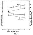
- Fig. 3 is a plot of the surface concentration of silicon and diffusion thickness of silicon, vs pressure in the enclosure (Torr) for 2 different silane flowrates : 4.2 sccm (dotted line) and 6.3 sccm (continuous line).
- Fig. 4 is a plot showing the effect of temperature in the enclosure (°C) on the surface concentration of silicon and diffusion thickness of silicon.
- Fig. 5,6, 7 show the silicon concentration profile at the surface of the sample and across the sample thickness for various CVD conditions.
- elemental analysis uses electron microprobe.
- Fig. 7 represents the layer electron depth profile (Sputter speed is 18 A/min).
- the present invention is a method of forming a silicon diffusion coating and/or overlay coating on the surface of a metallic sample, preferably iron base sample, comprising the treatment of said sample in a cold wall, low pressure CVD enclosure under an atmosphere comprising silane or a silicon hydride alone or a mixture of silane or a silicon hydride with an inert gas such as Helium or Argon or reducing gas such as hydrogen capable of reacting with the remaining oxygen species in the enclosure to avoid oxidation of the surface of the sample.
- the temperature in the enclosure is maintained between about 50°C and 1000°C as disclosed above, while the pressure is maintained as low as between about 0.1 Torr and about 100 Torr.
- Silicon hydride flow rate is varied according to the final desired diffusion thickness and silicon content at the surface. This flowrate is determined according to the size of the enclosure, and of sample itself in order to ensure the above pressure limits.
- the reaction time in the enclosure depends on the gas flowrate, pressure temperature etc..., and can be as short as about 20mm for formation of a layer of more than 100 ⁇ m thickness. It is usually preferred to make first a surface cleaning of the sample surface onto and through which silicon is deposited and diffused. This surface cleaning is preferably a mechanical polishing or a chemical etching or ultrasonic cleaning in an hydrous acetone or any other means, known per se. The best results have been obtained with a process comprising a mechanical polishing to obtain a mirror polished surface, followed by a chemical ultrasonic cleaning.
- silicon concentration on the surface, silicon profile in the sample and diffusion thickness are controllable up to 100% for the concentration and up to several mm for the diffusion thickness.
- This overlay coating can be further oxidized and/or submitted to a further step of oxidation or nitridation, to obtain surface properties which are known per se.
- the sample is first cleaned with an organic solvent and mechanically polished to mirror surface (preferably with a final stage of polishing being done with 0.3 micron Al2O3) or cleaned with an acidic solution.
- the substrate is heated up to CVD temperature under vacuum or inert gas residual pressure of about 0.5 Torr.
- the sample is then ready for surface treatment ; silane gas alone or a mixture of silane gas and another gas selected from the group comprising Helium, Argon, Hydrogen or a mixture thereof is injected in the enclosure, while maintaining the pressure lower than 100 Torr to make simultaneous silicon deposition and diffusion.
- This first example is directed to the production of a material having utility more particularly for electro-magnetic applications i.e. obtaining a layer containing uniformely approximately 6.5 wt% silicon over a thickness of a few hundred ⁇ m at the surface of an iron or iron-silicon alloy substrate.
- the substrate or sample is first mechanically polished with an abrasive powder of a very small diameter, comprising alumina and, diamond powders. After obtaining a mirror finish on the surface of the substrate where silicon has to be deposited, said substrate is further ultrasonically cleaned in anhydrous acetone.
- the sample is introduced in the enclosure which is evacuated during 5 minutes at a pressure which is lower that 0.5 Torr (preferably 0.1 Torr), the temperature being room temperature, then the sample is heated at a temperature greater than 700°C and preferably about 800°C, under a residual inert gas atmosphere at a pressure lower than 0.5 Torr in order to maintain the sample cleanness.
- 0.5 Torr preferably 0.1 Torr
- the next step consists in maintaining the temperature within the above range higher than 700°C and preferably by 800°C, while silane (or silicon hydrides) alone or with a diluting gas (He, Ar, H2or a mixture thereof) is injected in the enclosure with an enclosure pressure which is between about 0.5 Torr and 2.0 Torr.
- the silane flow rate is approximately 2 to 6 sccm pure or diluted by above gases.
- a uniform diffusion thickness of 50 to 100 ⁇ m is thus obtained in 20 mn (Fig.2).
- the diffused layer thickness is linear with CVD treatment duration from a few minutes up to several hours and is uniform in silicon concentration (Fig.5).
- the diffusion thickness and the Si concentration in the sample are controlled only by the net flow rate of SiH4 ; it does not make substantial difference to dilute SiH4 with Ar, He and/or H2 or to use it alone (Fig. 1,2).
- the silicon concentration in the diffusion layer increases slightly with total pressure whereas the thickness of the diffusion layer is essentially constant (Fig.3). Tests also have indicated that the pressure within the above defined range has no significant effect on the properties of the treated sample, except that the lower the pressure is, the smoother the surface of the sample is.
- This second example is particularly directed to the production of chemically functional surfaces, e.g. corrosion resistant and gas adsorption controlled surfaces on iron, iron base alloys and stainless steel substrates.
- chemically functional surfaces e.g. corrosion resistant and gas adsorption controlled surfaces on iron, iron base alloys and stainless steel substrates.
- this involves surfaces with high silicon concentration, i.e. above 7%, preferably above 14.5 wt%.
- This result is obtained with a temperature range of the CVD process comprised between 300 and 500°C.
- Corrosion resistant and adsorption controlled properties are achieved by the silicon rich surface and the good adhesion of that layer to the substrate is insured by silicon concentration gradient between the substrate and the surface of the metallic sample.
- Polishing, cleaning, outgassing and heating conditions of the sample before silane injection in the enclosure are similar to those given in example 1 (mirror polishing, ultrasonic cleaning in solvent and outgassing during 5 mn at a pressure lower than 0,5T at a temperature between room temperature and 300°C, substrate temperature is about 800°C, pressure is below 0.5 T, with residual atmosphere being preferably inert gas such as He or Argon or a mixture thereof).
- Fig.4 illustrates the relationship of the silicon content and diffusion and/or deposition thickness with the substrate temperature.
- the silicon surface concentration and the thickness of the diffusion layer increase with temperature (Fig.4)
- Fig.6 illustrates one example of the depth dependance of the silicon concentration in the diffusion layer. It shows a high silicon concentration at the outer surface, which corresponds to Fe-silicon rich intermetallic phases.
- the surface is connected continuously to the substrate via a silicon concentration gradient, hence insuring for adhesion between the surface layer and the substrate.
- the third example is particularly directed to the production of chemically functional surfaces, i.e. corrosion resistant materials, on iron, iron base alloys and stainless steels. This is achieved by formation of an overlay coating consisting of silicon, silicon oxide, silicon nitride or alloy of these compounds on top of above materials, with said overlay coating connected to substrate by a continuous silicon-concentration gradient across the interface.
- the preparation step of the sample in the CVD enclosure is as disclosed in example 1.
- the CVD step for diffusion and overlay coating under silane atmosphere is performed at a CVD temperature between 50°C and 300°C, preferably between 200 and 300°C with a silane flow rate of up to 20 sccm and a total pressure between abot 0.5 and 100 Torr.
- Fig. 7 shows the silicon concentration dependance across the sample thickness as obtained by Auger electron spectroscopy.
- An overlayer being essentially a silicon compound only is coated on a thin Fe-Si diffusion layer on top of the iron substrate.
- This example concerns the manufacture of Stainless Steel Piping for ultra high purity gas distribution. This is achieved by minimizing the molecular adsorption phenomena on the metallic wall, particularly for polar molecules such as H2O, and by strong corrosion resistance of surfaces for handling inert and corrosive gases respectively.
- the above goal is reached through formation of FeSi x intermetallic phase diffusion layers containing above 14.5 wt% Si on the inner surface of stainless steel pipes such as 316LSS electropolished pipe.
- the preparation step of sample is as in example 1 by pumping on the heated tubing.
- the CVD step for diffusion coating is performed at a CVD temperature between 300 and 700°C, preferably 400 to 500 °C, with a Silane flow rate of 1 to 20 sccm and a pressure between 0.5 and 100 Torr, preferably between 1 and 20 Torr.
- tubings reveal significantly improved adsorption properties of polar impurities present in carrier gases, particularly H2O.
- carrier gases particularly H2O.
- the total quantity of H2O adsorbed on a given piping area is decreased by more than one order of magnitude in comparison to electropolished piping. This is particularly useful for construction of ultrahigh purity gas distribution systems and the process is applicable to piping, cylinder, valves and other distribution component internal surfaces.
- the diffusion coating obtained is less uniform with some spots of different thickness. This coating is not satisfactory.
- the coatings are not good due to the presence of both diffusion coated and overlay coated spots.
Landscapes
- Chemical & Material Sciences (AREA)
- Chemical Kinetics & Catalysis (AREA)
- Engineering & Computer Science (AREA)
- Materials Engineering (AREA)
- Mechanical Engineering (AREA)
- Metallurgy (AREA)
- Organic Chemistry (AREA)
- General Chemical & Material Sciences (AREA)
- Inorganic Chemistry (AREA)
- Chemical Vapour Deposition (AREA)
- Solid-Phase Diffusion Into Metallic Material Surfaces (AREA)
Applications Claiming Priority (2)
| Application Number | Priority Date | Filing Date | Title |
|---|---|---|---|
| US68648791A | 1991-04-17 | 1991-04-17 | |
| US686487 | 1991-04-17 |
Publications (2)
| Publication Number | Publication Date |
|---|---|
| EP0509907A1 true EP0509907A1 (de) | 1992-10-21 |
| EP0509907B1 EP0509907B1 (de) | 1995-10-11 |
Family
ID=24756492
Family Applications (1)
| Application Number | Title | Priority Date | Filing Date |
|---|---|---|---|
| EP19920401046 Expired - Lifetime EP0509907B1 (de) | 1991-04-17 | 1992-04-15 | CVD-Verfahren zum Herstellen einer Siliziumdiffusionsschicht und/oder Überzug auf der Oberfläche eines Metallsubstrates |
Country Status (4)
| Country | Link |
|---|---|
| EP (1) | EP0509907B1 (de) |
| JP (1) | JPH05132777A (de) |
| CA (1) | CA2066100A1 (de) |
| DE (1) | DE69205320T2 (de) |
Cited By (4)
| Publication number | Priority date | Publication date | Assignee | Title |
|---|---|---|---|---|
| WO2006045576A3 (de) * | 2004-10-27 | 2006-07-20 | Univ Stuttgart | Verfahren zum korrosionsschutz von bauteilen aus warmfestem stahl |
| WO2014000963A1 (de) * | 2012-06-29 | 2014-01-03 | Robert Bosch Gmbh | Verfahren zum bearbeiten der oberfläche eines bauteils |
| CN113182731A (zh) * | 2021-05-08 | 2021-07-30 | 广西辉煌耐磨技术股份有限公司 | 高性能硬面堆焊药芯焊丝 |
| CN116641035A (zh) * | 2023-07-26 | 2023-08-25 | 南京诺源医疗器械有限公司 | 一种用于腹腔镜光学件的镀膜方法 |
Families Citing this family (3)
| Publication number | Priority date | Publication date | Assignee | Title |
|---|---|---|---|---|
| US5503383A (en) * | 1994-06-27 | 1996-04-02 | Kabushiki Kaisha Ace Denken | Ground mechanism for a paper strip conveying mechanism |
| JP5412462B2 (ja) | 2011-04-19 | 2014-02-12 | 日本パーカライジング株式会社 | 金属材料用耐食合金コーティング膜及びその形成方法 |
| CN110144567B (zh) * | 2019-06-06 | 2021-01-08 | 中国科学院金属研究所 | 采用化学气相沉积工艺在硅基体上制备超厚碳化硅梯度涂层的方法 |
Citations (3)
| Publication number | Priority date | Publication date | Assignee | Title |
|---|---|---|---|---|
| EP0226130A2 (de) * | 1985-12-11 | 1987-06-24 | Air Products And Chemicals, Inc. | Verfahren zum Herstellen einer Siliziumdiffusionsschicht auf metallischen Werkstücken |
| DE3726724A1 (de) * | 1986-08-11 | 1988-02-25 | Toshiba Kk | Elektrophotographisches aufzeichungsmaterial |
| EP0409687A1 (de) * | 1989-07-19 | 1991-01-23 | L'air Liquide, Societe Anonyme Pour L'etude Et L'exploitation Des Procedes Georges Claude | Verfahren zum Aufsilizieren von metallischen Gegendstand durch chemische Abscheidung aus der Dampfphase |
-
1992
- 1992-04-15 DE DE1992605320 patent/DE69205320T2/de not_active Expired - Fee Related
- 1992-04-15 JP JP9567692A patent/JPH05132777A/ja active Pending
- 1992-04-15 EP EP19920401046 patent/EP0509907B1/de not_active Expired - Lifetime
- 1992-04-15 CA CA 2066100 patent/CA2066100A1/en not_active Abandoned
Patent Citations (3)
| Publication number | Priority date | Publication date | Assignee | Title |
|---|---|---|---|---|
| EP0226130A2 (de) * | 1985-12-11 | 1987-06-24 | Air Products And Chemicals, Inc. | Verfahren zum Herstellen einer Siliziumdiffusionsschicht auf metallischen Werkstücken |
| DE3726724A1 (de) * | 1986-08-11 | 1988-02-25 | Toshiba Kk | Elektrophotographisches aufzeichungsmaterial |
| EP0409687A1 (de) * | 1989-07-19 | 1991-01-23 | L'air Liquide, Societe Anonyme Pour L'etude Et L'exploitation Des Procedes Georges Claude | Verfahren zum Aufsilizieren von metallischen Gegendstand durch chemische Abscheidung aus der Dampfphase |
Non-Patent Citations (1)
| Title |
|---|
| JOURNAL OF THE ELECTROCHEMICAL SOCIETY vol. 128, no. 6, 1 June 1981, MANCHESTER N.H. USA pages 1368 - 1373; M.J.RICE ET AL.: 'INTERACTION OF CVD SILICON WITH MOLYBDENUM SUBSTRATES.' * |
Cited By (5)
| Publication number | Priority date | Publication date | Assignee | Title |
|---|---|---|---|---|
| WO2006045576A3 (de) * | 2004-10-27 | 2006-07-20 | Univ Stuttgart | Verfahren zum korrosionsschutz von bauteilen aus warmfestem stahl |
| WO2014000963A1 (de) * | 2012-06-29 | 2014-01-03 | Robert Bosch Gmbh | Verfahren zum bearbeiten der oberfläche eines bauteils |
| CN113182731A (zh) * | 2021-05-08 | 2021-07-30 | 广西辉煌耐磨技术股份有限公司 | 高性能硬面堆焊药芯焊丝 |
| CN116641035A (zh) * | 2023-07-26 | 2023-08-25 | 南京诺源医疗器械有限公司 | 一种用于腹腔镜光学件的镀膜方法 |
| CN116641035B (zh) * | 2023-07-26 | 2023-10-13 | 南京诺源医疗器械有限公司 | 一种用于腹腔镜光学件的镀膜方法 |
Also Published As
| Publication number | Publication date |
|---|---|
| CA2066100A1 (en) | 1992-10-18 |
| JPH05132777A (ja) | 1993-05-28 |
| EP0509907B1 (de) | 1995-10-11 |
| DE69205320T2 (de) | 1996-03-14 |
| DE69205320D1 (de) | 1995-11-16 |
Similar Documents
| Publication | Publication Date | Title |
|---|---|---|
| US5198285A (en) | Hard and lubricant thin film of iron base metallic material coated with amorphous carbon-hydrogen-silicon | |
| Zhang et al. | TiN coating of tool steels: a review | |
| Haubner et al. | Diamond deposition on hardmetal substrates–Comparison of substrate pre-treatments and industrial applications | |
| AU619272B2 (en) | A surface-coated cemented carbide and a process for the production of the same | |
| EP1598441B1 (de) | Film aus amorphem kohlenstoff und herstellungsverfahren dafür | |
| EP1953258B1 (de) | Texturgehärtetes Alpha-Aluminium-beschichtetes Werkzeug | |
| US6040012A (en) | Process for the preparation by chemical vapor deposition (CVD) of a Ti-A1-N based multilayer coating | |
| US2962388A (en) | Process for the production of titanium carbide coatings | |
| JP4850074B2 (ja) | 研磨剤を被覆する方法 | |
| Bonnet et al. | Characterization of thin solid films of rare earth oxides formed by the metallo-organic chemical vapour deposition technique, for high temperature corrosion applications | |
| Nesladek et al. | Improved adhesion of CVD diamond films to steel and WC Co substrates | |
| EP0328084A2 (de) | Erosions- und verschleissfestes Verbundbeschichtungssystem | |
| CN1463303A (zh) | 复合材料及其制备方法 | |
| US5254369A (en) | Method of forming a silicon diffusion and/or overlay coating on the surface of a metallic substrate by chemical vapor deposition | |
| EP0509907B1 (de) | CVD-Verfahren zum Herstellen einer Siliziumdiffusionsschicht und/oder Überzug auf der Oberfläche eines Metallsubstrates | |
| JPH03240957A (ja) | 潤滑性を有する硬質非晶質炭素―水素―珪素薄膜、表面に該薄膜を有する鉄系金属材料、およびその製造方法 | |
| JP3214891B2 (ja) | ダイヤモンド類被覆部材 | |
| US5262202A (en) | Heat treated chemically vapor deposited products and treatment method | |
| US6365230B1 (en) | Method of manufacturing a diamond film coated cutting tool | |
| Li et al. | The effects of ion bombarding energy on the structure and properties of TiN films synthesized by dual ion beam sputtering | |
| Haubner et al. | Interactions of hard metal substrates during diamond deposition | |
| JP3081765B2 (ja) | 炭素部材およびその製造方法 | |
| US4873152A (en) | Heat treated chemically vapor deposited products | |
| Hirotaka Hamamura et al. | TiN films prepared by flow modulation chemical vapor deposition using TiCl4 and NH3 | |
| JP4666241B2 (ja) | 摺動部材 |
Legal Events
| Date | Code | Title | Description |
|---|---|---|---|
| PUAI | Public reference made under article 153(3) epc to a published international application that has entered the european phase |
Free format text: ORIGINAL CODE: 0009012 |
|
| 17P | Request for examination filed |
Effective date: 19920421 |
|
| AK | Designated contracting states |
Kind code of ref document: A1 Designated state(s): DE FR GB IT SE |
|
| 17Q | First examination report despatched |
Effective date: 19941216 |
|
| GRAA | (expected) grant |
Free format text: ORIGINAL CODE: 0009210 |
|
| AK | Designated contracting states |
Kind code of ref document: B1 Designated state(s): DE FR GB IT SE |
|
| ET | Fr: translation filed | ||
| ITF | It: translation for a ep patent filed | ||
| REF | Corresponds to: |
Ref document number: 69205320 Country of ref document: DE Date of ref document: 19951116 |
|
| PG25 | Lapsed in a contracting state [announced via postgrant information from national office to epo] |
Ref country code: SE Effective date: 19960111 |
|
| PLBE | No opposition filed within time limit |
Free format text: ORIGINAL CODE: 0009261 |
|
| STAA | Information on the status of an ep patent application or granted ep patent |
Free format text: STATUS: NO OPPOSITION FILED WITHIN TIME LIMIT |
|
| 26N | No opposition filed | ||
| PGFP | Annual fee paid to national office [announced via postgrant information from national office to epo] |
Ref country code: FR Payment date: 19980312 Year of fee payment: 7 |
|
| PGFP | Annual fee paid to national office [announced via postgrant information from national office to epo] |
Ref country code: GB Payment date: 19980320 Year of fee payment: 7 |
|
| PGFP | Annual fee paid to national office [announced via postgrant information from national office to epo] |
Ref country code: DE Payment date: 19980325 Year of fee payment: 7 |
|
| PG25 | Lapsed in a contracting state [announced via postgrant information from national office to epo] |
Ref country code: GB Free format text: LAPSE BECAUSE OF NON-PAYMENT OF DUE FEES Effective date: 19990415 |
|
| GBPC | Gb: european patent ceased through non-payment of renewal fee |
Effective date: 19990415 |
|
| PG25 | Lapsed in a contracting state [announced via postgrant information from national office to epo] |
Ref country code: FR Free format text: LAPSE BECAUSE OF NON-PAYMENT OF DUE FEES Effective date: 19991231 |
|
| REG | Reference to a national code |
Ref country code: FR Ref legal event code: ST |
|
| PG25 | Lapsed in a contracting state [announced via postgrant information from national office to epo] |
Ref country code: DE Free format text: LAPSE BECAUSE OF NON-PAYMENT OF DUE FEES Effective date: 20000201 |
|
| PG25 | Lapsed in a contracting state [announced via postgrant information from national office to epo] |
Ref country code: IT Free format text: LAPSE BECAUSE OF NON-PAYMENT OF DUE FEES;WARNING: LAPSES OF ITALIAN PATENTS WITH EFFECTIVE DATE BEFORE 2007 MAY HAVE OCCURRED AT ANY TIME BEFORE 2007. THE CORRECT EFFECTIVE DATE MAY BE DIFFERENT FROM THE ONE RECORDED. Effective date: 20050415 |