EP0509799A2 - Circuit de multiplexage à division temporelle à efficience elevée - Google Patents
Circuit de multiplexage à division temporelle à efficience elevée Download PDFInfo
- Publication number
- EP0509799A2 EP0509799A2 EP92303407A EP92303407A EP0509799A2 EP 0509799 A2 EP0509799 A2 EP 0509799A2 EP 92303407 A EP92303407 A EP 92303407A EP 92303407 A EP92303407 A EP 92303407A EP 0509799 A2 EP0509799 A2 EP 0509799A2
- Authority
- EP
- European Patent Office
- Prior art keywords
- nth
- data
- time
- time period
- available
- Prior art date
- Legal status (The legal status is an assumption and is not a legal conclusion. Google has not performed a legal analysis and makes no representation as to the accuracy of the status listed.)
- Withdrawn
Links
Images


Classifications
-
- H—ELECTRICITY
- H04—ELECTRIC COMMUNICATION TECHNIQUE
- H04J—MULTIPLEX COMMUNICATION
- H04J3/00—Time-division multiplex systems
- H04J3/02—Details
- H04J3/06—Synchronising arrangements
- H04J3/062—Synchronisation of signals having the same nominal but fluctuating bit rates, e.g. using buffers
- H04J3/0626—Synchronisation of signals having the same nominal but fluctuating bit rates, e.g. using buffers plesiochronous multiplexing systems, e.g. plesiochronous digital hierarchy [PDH], jitter attenuators
- H04J3/0629—Synchronisation of signals having the same nominal but fluctuating bit rates, e.g. using buffers plesiochronous multiplexing systems, e.g. plesiochronous digital hierarchy [PDH], jitter attenuators in a network, e.g. in combination with switching or multiplexing, slip buffers
-
- H—ELECTRICITY
- H04—ELECTRIC COMMUNICATION TECHNIQUE
- H04J—MULTIPLEX COMMUNICATION
- H04J3/00—Time-division multiplex systems
- H04J3/16—Time-division multiplex systems in which the time allocation to individual channels within a transmission cycle is variable, e.g. to accommodate varying complexity of signals, to vary number of channels transmitted
- H04J3/1682—Allocation of channels according to the instantaneous demands of the users, e.g. concentrated multiplexers, statistical multiplexers
Definitions
- the present invention relates to a data multiplexing apparatus for time-division multiplexing a plurality of kinds of data blocks.
- time-division data multiplexing apparatus has a circuit arrangement as shown in Fig.5.
- This apparatus is shown in "Technology of PCM communications" by Kaneko, Sanpo Publishing Co., P.11, 1983. The operation of the apparatus will be explained with reference to Fig.6.
- a 4-step rotary switch 7 rotates at a constant speed of one rotation per given period T, first through fourth discrete data blocks are sequentially selected at time intervals of T/4 to form a time-division multiplexed data.
- the size of the time slot assigned to each data block is fixed (T/4 in the above case). So, when the data size of each data block is not uniform or varies with time, the rotating period T of the rotary switch must be set so that each time slot can accommodate a data block having a maximum data size. Since such a large time slot is assigned equally to every data block, which has a smaller data size in most cases, unoccupied time will increase. Accordingly, a highly efficient time-division data multiplexing cannot be expected.
- N) address control circuit of the first through Nth address control circuits comprising means for calculating a time period A n of an nth time slot to be assigned to a corresponding nth data block from a data size M n of the nth data block stored in a corresponding nth memory and an available time period T n indicated by an available time signal as a time period available for transmission of the nth through Nth data blocks, and means for controlling the nth memory so as to read out data of the nth data block stored in the nth memory for the time period A n and for outputting for the time period A n a selection signal S n indicating that the nth data block stored in the nth memory is being read out; and a selecting means coupled to the first through Nth memories and responsive to the nth selection signal for selectively outputting the nth data block read out from the nth memory to form a time-division multiplexed data which are composed of the first through Nth data blocks which are respectively assigned to first
- An available time signal indicative of a time period available for transmission of the first through Nth data blocks may be externally given to the first address control circuit.
- a length of each time slot assigned to a corresponding data block can be determined according to a data size of the corresponding data block. Accordingly, a highly efficient time-division data multiplexing can be realized.
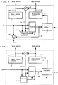
- Fig. 1 is a schematic block diagram showing a time-division data multiplexing apparatus as an embodiment of the present invention
- Fig.2 is a schematic timing chart showing a multiplexed data stream produced by the apparatus shown in Fig. 1. It is assumed that n input data blocks, first through Nth data blocks, are to be time-division multiplexed. The data transmission rate is assumed to be constant. A quantity of data transmitted in a predetermined time period T is expressed as Q T . A total quantity (total data size) of the first through Nth data blocks is assumed to be Q T .
- the input first through Nth data blocks (N is an integer of at least 2) are temporarily stored in first through Nth memories 1, 3 and 5, respectively.
- the first through Nth memories are controlled by first through Nth address control circuits 2, 4 and 6, respectively.
- the nth memory 3 stores the nth input data block.
- the first address control circuit 2 receives an available-time signal T 1 which is equal to a total time period T available for transmission of the total N input data blocks, and calculates a time period A 1 of a time slot to be assigned to the first data block from the time period T 1 (here, both an available-time signal and a time period indicated by the signal are denoted by the same reference symbol) and a data size M 1 of the first data block stored in the first memory 1. According to the time period A 1 , the first address control circuit 2 controls the first memory 1 to read out the stored first data block, and at the same time outputs a selection signal S 1 indicating that the first data block is selected for transmission.
- a selector 7 selects output data D 1 from the first memory 1 as a data block to be transmitted in response to the selection signal S 1 , and passes therethrough the output data D 1 from the first memory 1, i.e., data in the first data block. Further, the first address control circuit 2 calculates a difference between the time period T 1 and the time period A 1 and generates an available-time signal T 2 indicative of the difference. The available-time signal T 2 is received by the second address control circuit (not shown in Fig.1).
- the nth address control circuit 4 receives an available-time signal T n indicative of a time period available for transmission of the nth through Nth data blocks, and calculates a time period A n of a time slot to be assigned to the nth data block from the time period T n and a data size M n of the nth data block stored in the nth memory 3. According to the time period A n , the nth address control circuit 4 controls the nth memory 3 to read out the stored nth data block, and at the same time outputs a selection signal S n indicating that the nth data block is selected for transmission.
- a selector 7 selects output data D n from the nth memory 3 as a data block to be transmitted in response to the selection signal S n , and passes therethrough the output data D n from the nth memory 3, i.e., data in the nth data block. Further the nth address control circuit 4 calculates a difference between the time period T n and the time period A n and generates an available-time signal T n+1 indicative of the difference. The available-time signal T n+1 is received by the (n+1)th address control circuit (not shown in Fig. 1). Of course, it is not necessary for the Nth address control circuit 6 to output an available-time signal because there is no signal block remaining.
- the output data from the selector 7 becomes a time-division multiplexed data D in which the first through Nth data blocks are sequentially time-division multiplexed in the predetermined time period T as shown in Fig.2.
- Each time slot assigned to a corresponding data block has a time period which is determined depending upon the data size of the corresponding data block. It may be understood that there is no time slot which has an unoccupied portion in which no data exist.
- each of the first through Nth memories in Fig. 1 is assumed to be a first-in first-out memory (FIFO memory, hereafter).
- a write address counter 41 and a read address counter 42 respectively generate a write address Aw n and a read address Ar n of the nth FIFO memory.
- the data size of the nth data block stored in the nth FIFO memory 1 or 3 can be represented by a difference between the read address Ar n and write address Aw n .
- a subtractor 43 calculates the difference between the read address Ar n and write address Aw n and outputs a difference signal M n indicative of the difference, or the data size of the nth data block stored in the nth FIFO memory.
- a comparator 44 compares the difference signal M n with the available-time signal T n indicative of the time period T n assigned for transmission of the nth through Nth data blocks and outputs a signal indicating which of M n and T n is smaller than the other.
- a selector 45 receives the difference signal M n and the available-time signal T n and selects as an output signal A n thereof a smaller one of the two signals according to the output signal of the comparator 44.
- the selector 45 outputs the difference signal M n when M n is smaller than T n and the available-time signal T n when T n is smaller than M n .
- the output signal A n of the selector 45 indicates a time period A n of the time slot assigned to the nth data block.
- a read data counter 46 is responsive to the output signal A n of the selector 45 for activating the read address counter 42 for the time period A n so as to read out the data of the data block D n stored in the nth memory 1 or 3, and for generating the selection signal S n for the time period A n . That is, the selection signal S n indicates that the nth data block is being selected as the data block to be transmitted.
- the selector 7 shown in Fig. 1 passes therethrough the output data D n from the nth memory 3 in response to the selection signal S n to allocate the data D n of the nth data block to the nth time slot having the time period A n .
- the new available-time signal Tn+1 is sent to the selector (corresponding to the selector 45) of the (n+1)th address control circuit.
- Fig.4 is a schematic block diagram showing an example of the Nth address control circuit in the apparatus shown in Fig.1.
- a write address counter 61 and a read address counter 62 respectively generate a write address Aw N and a read address Ar N of the Nth FIFO memory 5.
- the data size of the Nth data block stored in the Nth FIFO memory can be represented by a difference between the read address Ar N and write address Aw N .
- a subtractor 63 calculates the difference between the read address Ar N and write address Aw N and outputs a difference signal M N indicative of the difference, or the data size of the Nth data block stored in the Nth FIFO memory.
- a comparator 64 compares the difference signal M N with the available-time signal T N indicative of the time period T N assigned for transmission of the Nth data block and outputs a signal indicating which of M N and T N is smaller than the other.
- a selector 65 receives the difference signal M N and the available-time signal T N and selects as an output signal A N thereof a smaller one of the two signals according to the output signal of the comparator 64. That is, the selector 65 outputs the difference signal M N when M N is smaller than T N and the available-time signal T N when T N is smaller than M N .
- the output signal A N of the selector 65 indicates a time period A N of the time slot assigned to the Nth data block.
- a read data counter 66 is responsive period A N so as to read out the data of the data block D N stored in the Nth memory, and for generating the selection signal S N for the time period A N . That is, the selection signal S N indicates that the Nth data block is being selected as the data block to be transmitted.
- the selector 7 shown in Fig.1 passes therethrough the output data D N from the Nth memory 5 in response to the selection signal S N to allocate the data D N of the Nth data block to the Nth time slot having the time period A N .
- a time-division data multiplexing apparatus determines a data size of each data block from read and write address of a corresponding memory storing the data block, and decides a length of a time slot to be assigned to the data block from the data size of the data block and an available time for transmission of the data block and succeeding data blocks. Further, the remainder of the available time is assigned to the succeeding data blocks. Accordingly, each time slot is assigned to a corresponding data block according to the data size of the data block so as to perform time-division data multiplexing at high efficiency without causing a loss time.
Landscapes
- Engineering & Computer Science (AREA)
- Computer Networks & Wireless Communication (AREA)
- Signal Processing (AREA)
- Computer Hardware Design (AREA)
- Time-Division Multiplex Systems (AREA)
Applications Claiming Priority (2)
| Application Number | Priority Date | Filing Date | Title |
|---|---|---|---|
| JP86707/91 | 1991-04-18 | ||
| JP3086707A JPH07112181B2 (ja) | 1991-04-18 | 1991-04-18 | データ多重化回路 |
Publications (2)
| Publication Number | Publication Date |
|---|---|
| EP0509799A2 true EP0509799A2 (fr) | 1992-10-21 |
| EP0509799A3 EP0509799A3 (en) | 1993-01-13 |
Family
ID=13894393
Family Applications (1)
| Application Number | Title | Priority Date | Filing Date |
|---|---|---|---|
| EP19920303407 Withdrawn EP0509799A3 (en) | 1991-04-18 | 1992-04-15 | Highly-efficient time-division data multiplexing apparatus |
Country Status (3)
| Country | Link |
|---|---|
| US (1) | US5311517A (fr) |
| EP (1) | EP0509799A3 (fr) |
| JP (1) | JPH07112181B2 (fr) |
Families Citing this family (11)
| Publication number | Priority date | Publication date | Assignee | Title |
|---|---|---|---|---|
| JPH06191093A (ja) * | 1992-12-25 | 1994-07-12 | Fuji Xerox Co Ltd | 記録装置 |
| JP3778993B2 (ja) * | 1995-05-16 | 2006-05-24 | ヒューレット・パッカード・カンパニー | 最小論理マルチプレクサ・システム |
| US5602848A (en) * | 1995-06-05 | 1997-02-11 | International Business Machines Corporation | Multi-mode TDM interface circuit |
| FI101120B (fi) | 1995-09-05 | 1998-04-15 | Nokia Telecommunications Oy | Yhden bitin resoluutiolla kytkevä kytkentäkenttä |
| JPH1168797A (ja) * | 1997-08-26 | 1999-03-09 | Nec Corp | 可変長セル対応位相乗換装置 |
| US6295299B1 (en) * | 1997-08-29 | 2001-09-25 | Extreme Networks, Inc. | Data path architecture for a LAN switch |
| US6246681B1 (en) * | 1997-12-19 | 2001-06-12 | Alcatel Usa Sourcing, L.P. | System and method for plane selection |
| US7187673B2 (en) * | 2000-12-18 | 2007-03-06 | Koninklijke Philips Electronics N.V. | Technique for creating a machine to route non-packetized digital signals using distributed RAM |
| JP4664252B2 (ja) * | 2006-07-31 | 2011-04-06 | 富士通株式会社 | 監視ユニット及び被監視ユニット |
| KR101346162B1 (ko) * | 2007-02-28 | 2014-01-06 | 삼성전자주식회사 | 데이터 버스트를 처리하는 데이터 버스트 어셈블리 장치 및그 방법 |
| JP4998367B2 (ja) * | 2008-05-13 | 2012-08-15 | 日本電気株式会社 | データ伝送装置および帯域割当方法 |
Family Cites Families (12)
| Publication number | Priority date | Publication date | Assignee | Title |
|---|---|---|---|---|
| JPS5783945A (en) * | 1980-11-12 | 1982-05-26 | Mitsubishi Electric Corp | Information transmitter |
| JPS592455A (ja) * | 1982-06-28 | 1984-01-09 | Fujitsu Ltd | 時分割多重伝送方式 |
| GB8515347D0 (en) * | 1985-06-18 | 1985-07-17 | Plessey Co Plc | Telecommunications exchanges |
| EP0227852B1 (fr) * | 1985-12-23 | 1990-08-29 | International Business Machines Corporation | Système local de communication pour services intégrés basé sur un moyen de transmission à structure de boucle avec utilisation d'un jeton |
| US4727536A (en) * | 1986-06-19 | 1988-02-23 | General Datacomm, Inc. | Variable control and data rates in highly efficient multiplexer |
| CA1292333C (fr) * | 1987-05-15 | 1991-11-19 | Masayoshi Shimada | Systemes numeriques a multiplexage temporel et methode de controle de ces systemes |
| FR2618624B1 (fr) * | 1987-07-24 | 1992-04-30 | Michel Servel | Systeme de commutation de multiplex temporels hybrides a memoire tampon optimisee |
| US4893306A (en) * | 1987-11-10 | 1990-01-09 | Bell Communications Research, Inc. | Method and apparatus for multiplexing circuit and packet traffic |
| FR2623954B1 (fr) * | 1987-11-27 | 1993-11-19 | Alcatel Cit | Element de commutation de donnees transmises par multiplexage temporel asynchrone |
| US4891805A (en) * | 1988-06-13 | 1990-01-02 | Racal Data Communications Inc. | Multiplexer with dynamic bandwidth allocation |
| US5128929A (en) * | 1988-11-15 | 1992-07-07 | Nec Corporation | Time division switching system capable of broad band communications service |
| US5121383A (en) * | 1990-11-16 | 1992-06-09 | Bell Communications Research, Inc. | Duration limited statistical multiplexing in packet networks |
-
1991
- 1991-04-18 JP JP3086707A patent/JPH07112181B2/ja not_active Expired - Fee Related
-
1992
- 1992-04-15 EP EP19920303407 patent/EP0509799A3/en not_active Withdrawn
- 1992-04-20 US US07/870,632 patent/US5311517A/en not_active Expired - Fee Related
Also Published As
| Publication number | Publication date |
|---|---|
| JPH07112181B2 (ja) | 1995-11-29 |
| JPH04318717A (ja) | 1992-11-10 |
| EP0509799A3 (en) | 1993-01-13 |
| US5311517A (en) | 1994-05-10 |
Similar Documents
| Publication | Publication Date | Title |
|---|---|---|
| CA1292541C (fr) | Systeme de commutation hybride de signaux a multiplexage temporel a memoire tampon optimisee | |
| US6009108A (en) | Multiplexer system for converting variable-length burst data streams into averaged-transfer-rate fixed-length packets | |
| US6768734B2 (en) | Device and method for equalizing data delays | |
| EP0509799A2 (fr) | Circuit de multiplexage à division temporelle à efficience elevée | |
| US4815110A (en) | Method and a system for synchronizing clocks in a bus type local network | |
| JPH0568243A (ja) | 可変長符号化制御方式 | |
| US5128939A (en) | Method of phase-converting frame and apparatus using same | |
| US5351232A (en) | Path monitoring system for cross-connect system | |
| JPH03101537A (ja) | ビットレート適合用装置 | |
| US4680752A (en) | Time switch in a time division switching network | |
| US5548534A (en) | Two stage clock dejitter circuit for regenerating an E4 telecommunications signal from the data component of an STS-3C signal | |
| US6775294B2 (en) | Time slot assigner for communication system | |
| US5864536A (en) | Method and apparatus for adapting a transmission bit rate of a data multiplexer operating according to an asynchronous transfer mode | |
| EP0345891A1 (fr) | Système de commutation pour commuter des données orientées paquet aussi bien que circuit | |
| CA2070000C (fr) | Elements de commutation espace/temps | |
| US5654967A (en) | Delay-in-frames correcting system in a PCM transmission line | |
| US5287360A (en) | Device for inserting information bits into a specific frame structure | |
| EP0504710A1 (fr) | Commutateur à point de croisement utilisant des mémoires communes | |
| CA2243448A1 (fr) | Methode de commande de transmission de donnees a partir d'un dispositif comportant une pluralite de files d'attente | |
| KR960705428A (ko) | 동기회로장치(synchronizing circuit arrangement) | |
| CA1091832A (fr) | Appareil de decodage commun mic asynchrone | |
| EP0251588B1 (fr) | Multiplexeur entrelacé de bits avec synchronisation d'octets pour des équipements en communication | |
| US5257262A (en) | DCME unit capable of processing a wide variety of input information signals | |
| US5802358A (en) | Digital audio data phase shifting apparatus | |
| JP2933653B2 (ja) | パケットスイッチング交換装置の入力変換装置 |
Legal Events
| Date | Code | Title | Description |
|---|---|---|---|
| PUAI | Public reference made under article 153(3) epc to a published international application that has entered the european phase |
Free format text: ORIGINAL CODE: 0009012 |
|
| AK | Designated contracting states |
Kind code of ref document: A2 Designated state(s): DE FR GB |
|
| PUAL | Search report despatched |
Free format text: ORIGINAL CODE: 0009013 |
|
| AK | Designated contracting states |
Kind code of ref document: A3 Designated state(s): DE FR GB |
|
| STAA | Information on the status of an ep patent application or granted ep patent |
Free format text: STATUS: THE APPLICATION IS DEEMED TO BE WITHDRAWN |
|
| 18D | Application deemed to be withdrawn |
Effective date: 19930714 |