EP0509343A2 - Méthode de fonctionnement d'un régulateur à découpage et son dispositif - Google Patents
Méthode de fonctionnement d'un régulateur à découpage et son dispositif Download PDFInfo
- Publication number
- EP0509343A2 EP0509343A2 EP92105757A EP92105757A EP0509343A2 EP 0509343 A2 EP0509343 A2 EP 0509343A2 EP 92105757 A EP92105757 A EP 92105757A EP 92105757 A EP92105757 A EP 92105757A EP 0509343 A2 EP0509343 A2 EP 0509343A2
- Authority
- EP
- European Patent Office
- Prior art keywords
- switch
- actuator
- switching regulator
- current
- pulses
- Prior art date
- Legal status (The legal status is an assumption and is not a legal conclusion. Google has not performed a legal analysis and makes no representation as to the accuracy of the status listed.)
- Granted
Links
Images

Classifications
-
- H—ELECTRICITY
- H02—GENERATION; CONVERSION OR DISTRIBUTION OF ELECTRIC POWER
- H02M—APPARATUS FOR CONVERSION BETWEEN AC AND AC, BETWEEN AC AND DC, OR BETWEEN DC AND DC, AND FOR USE WITH MAINS OR SIMILAR POWER SUPPLY SYSTEMS; CONVERSION OF DC OR AC INPUT POWER INTO SURGE OUTPUT POWER; CONTROL OR REGULATION THEREOF
- H02M3/00—Conversion of dc power input into dc power output
- H02M3/22—Conversion of dc power input into dc power output with intermediate conversion into ac
- H02M3/24—Conversion of dc power input into dc power output with intermediate conversion into ac by static converters
- H02M3/28—Conversion of dc power input into dc power output with intermediate conversion into ac by static converters using discharge tubes with control electrode or semiconductor devices with control electrode to produce the intermediate ac
- H02M3/325—Conversion of dc power input into dc power output with intermediate conversion into ac by static converters using discharge tubes with control electrode or semiconductor devices with control electrode to produce the intermediate ac using devices of a triode or a transistor type requiring continuous application of a control signal
- H02M3/335—Conversion of dc power input into dc power output with intermediate conversion into ac by static converters using discharge tubes with control electrode or semiconductor devices with control electrode to produce the intermediate ac using devices of a triode or a transistor type requiring continuous application of a control signal using semiconductor devices only
- H02M3/33507—Conversion of dc power input into dc power output with intermediate conversion into ac by static converters using discharge tubes with control electrode or semiconductor devices with control electrode to produce the intermediate ac using devices of a triode or a transistor type requiring continuous application of a control signal using semiconductor devices only with automatic control of the output voltage or current, e.g. flyback converters
-
- Y—GENERAL TAGGING OF NEW TECHNOLOGICAL DEVELOPMENTS; GENERAL TAGGING OF CROSS-SECTIONAL TECHNOLOGIES SPANNING OVER SEVERAL SECTIONS OF THE IPC; TECHNICAL SUBJECTS COVERED BY FORMER USPC CROSS-REFERENCE ART COLLECTIONS [XRACs] AND DIGESTS
- Y02—TECHNOLOGIES OR APPLICATIONS FOR MITIGATION OR ADAPTATION AGAINST CLIMATE CHANGE
- Y02B—CLIMATE CHANGE MITIGATION TECHNOLOGIES RELATED TO BUILDINGS, e.g. HOUSING, HOUSE APPLIANCES OR RELATED END-USER APPLICATIONS
- Y02B70/00—Technologies for an efficient end-user side electric power management and consumption
- Y02B70/10—Technologies improving the efficiency by using switched-mode power supplies [SMPS], i.e. efficient power electronics conversion e.g. power factor correction or reduction of losses in power supplies or efficient standby modes
Definitions
- the invention relates to a method for operating a switching regulator.
- the length of the switch-on pulses for the actuator is usually regulated as a function of the output voltage and / or the current through the actuator (DE 27 15 571C2). It is known from EP 205 630 B1 to regulate the length of the switch-on pulses for the actuator as a function of the current through the actuator, the pause time between two switch-on pulses being kept constant. From IEEE Transactions on Power Electronics, Vol. PE-1, No. 3, July 86, pages 181 to 191, it is known to regulate the length of the switch-on pulses for the actuator depending on the level of the input voltage and the output voltage.
- the object of the invention is to provide a method for operating a switching regulator which can be used in particular for switching regulators with relatively high switching frequencies.
- Claim 5 shows a switching regulator which is particularly suitable for carrying out the method according to claim 1.
- the remaining claims relate to further development of the method / the switching regulator.
- the invention is based on the following findings: In the case of a forward control with a constant pause time for the switch-on pulses, the frequency variation is too strong, so that this type of switching regulator is not suitable for high-frequency applications.
- control delays often have an unfavorable effect.
- Complex auxiliary devices such as sawtooth generators with comparison devices and current detection devices, are not necessary in the invention.
- Switching regulators with switching frequencies of greater than 300 kHz can be constructed with the invention. Switching regulators with such switching frequencies have hitherto only been able to be implemented with resonance converters which, in addition to additional resonance-determining elements, generally require complex control circuits.
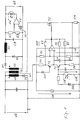
- Fig. 1 is a schematic diagram of a switching regulator for performing the method according to the invention.
- Fig. 2 shows the time course of the current through the switching regulator actuator.
- the input voltage UE of the switching regulator is to the series circuit, consisting of the primary winding W1 of the transformer Tr, the actuator TS - here designed as a field effect transistor - and the current measuring resistor RM.
- the secondary circuit of the switching regulator consists of the secondary winding W2 of the transformer Tr, the rectifier D1, the freewheeling diode D2, the smoothing choke Dr and the smoothing capacitor CA on the output side.
- the output voltage UA of the switching regulator for DC voltage consumers can be removed from the latter.
- a conventional demagnetization winding W3 with diode D3 is provided for demagnetizing the transformer Tr.
- the level of the output voltage UA of the switching regulator is detected by a first sensor - voltage divider R2, R3 and an error signal amplifier FV connected to it. As soon as the output voltage UA exceeds the value of the reference voltage Ur1 at the reference input of the error amplifier FV, a signal proportional to the level of the output voltage UA is transmitted to the primary control circuit via the optocoupler OK and is available there for regulating the repetition frequency of the switch-on pulses for the switching regulator actuator TS.
- the input voltage UE of the switching regulator is in the control loop at the series circuit consisting of the resistor R1, the switching section of the pnp switching section T2, the switching section of the npn switching section T3 and the resistor R4 as the first sensor.
- the actuator TS is controlled via an astable multivibrator MV, which is designed as a threshold comparator K with a charging capacitor C1 as a frequency-determining element.
- the inverting input of the threshold value comparator is connected both to the collectors of the transistors T2, T3 and to an electrode of the charging capacitor C1.
- the other electrode of the charging capacitor C1 leads to the connection point between the actuator - source of the n-channel field effect transistor - and current measuring resistor RM.
- the transistor T3, together with the Zener diode ZD2 also acts as a current source which can be controlled as a function of the output voltage UA.
- the output voltage UK of the optocoupler OK is led to the base of the transistor T2.
- the comparator H has H potential on the output side.
- the field effect transistor TS thus becomes conductive.
- the current source formed from the transistor T3 is then rendered ineffective via the voltage divider R5, R4, which lies between the output of the comparator K and the reference ground, by raising the emitter potential of the transistor T3 above the base potential, so that the transistor T3 blocks.
- the charging capacitor C1 was previously discharged to the lower switching threshold of the comparator K, which is predetermined by the circuitry of the comparator K with the resistors R6, R7 and R8.
- the charging capacitor C1 is now charged via the current source - transistor T2 - the charging current being controlled as a function of the level of the input voltage UE via the resistor R1. If the input voltage UE now becomes higher, the increase in the current IS through the actuator TS is steeper (dashed line in FIG. 2) than with a lower input voltage (solid line in FIG. 2). A higher charging current then flows, ie the inverting input of the threshold value comparator K reaches a higher one more quickly Potential as the non-inverting input.
- the astable multivibrator MV formed by the comparator K tilts earlier to L potential and thus shortens the switch-on time of the actuator TS from t L to t L '(FIG. 2).
- the emitter potential of the transistor T2 becomes more negative than the base potential via the resistors R9 and R1, as a result of which transistor T2 blocks and thus puts the charging current source out of operation.
- the current source - transistor T3 - is activated by connecting resistor R5 in parallel with emitter resistor R4 via the L potential at the output of comparator K. This reduces the emitter potential of transistor T3 and the current through the current source - transistor T3 - results from the voltage UK at the optocoupler, the base emitter voltage U BE of transistor T3 and the parallel connection of resistors R4, R5.
- the charging capacitor C1 is now discharged with this current up to the lower switching threshold of the comparator K.
- the time of the discharge t E or t E '(FIG. 2) of the charging capacitor C1 depends on the output voltage UA. This also determines the repetition frequency 1 / T of the switch-on pulses for the actuator TS. As can be seen from FIG. 2, the point in time at which the actuator TS is switched on again — end of the period T or T ′ — results from the intersection of a discharge characteristic curve with the lower threshold value SW for the comparator K. As FIG. 2 has further shown the discharge characteristics, in contrast to the charging characteristics, have the same slope.
- the switch-off time and thus the length of the switch-on pulses - end of the conduction time t L or t L 'for the actuator TS can also be controlled by the amount of the energy consumption current IS.
- the current measuring resistor RM which is connected in series with the charging capacitor C1
- the switch-off time of the actuator TS therefore depends on the sum of the variable dependent on the input voltage UE and the variable dependent on the energy consumption current IS.
- the influence of the input voltage UE on the switch-on time t L , t L ' is chosen, for example, so that when the input voltage UE varies, the repetition frequency 1 / T, 1 / T' is almost constant, the influence of the error amplifier FV when the output voltage is detected UA is also taken into account.
- This operating mode has the advantage of a simple load current limitation, which can also be connected to the base of transistor T3.
Landscapes
- Engineering & Computer Science (AREA)
- Power Engineering (AREA)
- Dc-Dc Converters (AREA)
Applications Claiming Priority (2)
| Application Number | Priority Date | Filing Date | Title |
|---|---|---|---|
| DE4112240A DE4112240A1 (de) | 1991-04-15 | 1991-04-15 | Verfahren zum betreiben eines schaltreglers sowie anordnung |
| DE4112240 | 1991-04-15 |
Publications (3)
| Publication Number | Publication Date |
|---|---|
| EP0509343A2 true EP0509343A2 (fr) | 1992-10-21 |
| EP0509343A3 EP0509343A3 (en) | 1992-11-19 |
| EP0509343B1 EP0509343B1 (fr) | 1996-07-17 |
Family
ID=6429605
Family Applications (1)
| Application Number | Title | Priority Date | Filing Date |
|---|---|---|---|
| EP92105757A Expired - Lifetime EP0509343B1 (fr) | 1991-04-15 | 1992-04-03 | Méthode de fonctionnement d'un régulateur à découpage et son dispositif |
Country Status (2)
| Country | Link |
|---|---|
| EP (1) | EP0509343B1 (fr) |
| DE (2) | DE4112240A1 (fr) |
Cited By (6)
| Publication number | Priority date | Publication date | Assignee | Title |
|---|---|---|---|---|
| EP0584623A1 (fr) * | 1992-08-28 | 1994-03-02 | Siemens Aktiengesellschaft | Convertisseur en courant continu à mode de courant |
| EP0657986A1 (fr) * | 1993-12-10 | 1995-06-14 | Siemens Aktiengesellschaft | Convertisseur à découpage avec coupleur optique |
| AT405704B (de) * | 1996-07-15 | 1999-11-25 | Siemens Ag Oesterreich | Schaltnetzteil |
| AT409202B (de) * | 1998-12-16 | 2002-06-25 | Siemens Ag Oesterreich | Schaltnetzteil |
| US6922287B2 (en) | 2001-10-12 | 2005-07-26 | Unaxis Balzers Aktiengesellschaft | Light coupling element |
| US10746000B2 (en) | 2016-02-17 | 2020-08-18 | Halliburton Energy Services, Inc. | Wide-input-range downhole power supply |
Citations (6)
| Publication number | Priority date | Publication date | Assignee | Title |
|---|---|---|---|---|
| US3373334A (en) * | 1965-06-01 | 1968-03-12 | Sperry Rand Corp | Regulated d.c. to d.c. power supply |
| US4037271A (en) * | 1976-12-03 | 1977-07-19 | Boschert Associates | Switching regulator power supply |
| DE2715571A1 (de) * | 1977-04-07 | 1978-10-12 | Licentia Gmbh | Verfahren zur steuerung eines schaltreglers |
| EP0205630A1 (fr) * | 1985-06-20 | 1986-12-30 | ANT Nachrichtentechnik GmbH | Régulateur de découpage et son application |
| US4648015A (en) * | 1984-10-04 | 1987-03-03 | Motorola, Inc. | Filter capacitor discharge circuit for a DC-DC converter |
| EP0259775A2 (fr) * | 1986-09-11 | 1988-03-16 | Siemens Aktiengesellschaft | Disposition de circuit pour limiter, réguler et dans certains cas interrompre le courant de collecteur du transistor de découpage placé dans le circuit primaire d'une alimentation à découpage |
Family Cites Families (1)
| Publication number | Priority date | Publication date | Assignee | Title |
|---|---|---|---|---|
| US3590361A (en) * | 1969-12-31 | 1971-06-29 | Bell Telephone Labor Inc | Dc to dc converter including switching device having its on and off times independently controlled by the line and load voltages, respectively |
-
1991
- 1991-04-15 DE DE4112240A patent/DE4112240A1/de not_active Ceased
-
1992
- 1992-04-03 EP EP92105757A patent/EP0509343B1/fr not_active Expired - Lifetime
- 1992-04-03 DE DE59206766T patent/DE59206766D1/de not_active Expired - Fee Related
Patent Citations (6)
| Publication number | Priority date | Publication date | Assignee | Title |
|---|---|---|---|---|
| US3373334A (en) * | 1965-06-01 | 1968-03-12 | Sperry Rand Corp | Regulated d.c. to d.c. power supply |
| US4037271A (en) * | 1976-12-03 | 1977-07-19 | Boschert Associates | Switching regulator power supply |
| DE2715571A1 (de) * | 1977-04-07 | 1978-10-12 | Licentia Gmbh | Verfahren zur steuerung eines schaltreglers |
| US4648015A (en) * | 1984-10-04 | 1987-03-03 | Motorola, Inc. | Filter capacitor discharge circuit for a DC-DC converter |
| EP0205630A1 (fr) * | 1985-06-20 | 1986-12-30 | ANT Nachrichtentechnik GmbH | Régulateur de découpage et son application |
| EP0259775A2 (fr) * | 1986-09-11 | 1988-03-16 | Siemens Aktiengesellschaft | Disposition de circuit pour limiter, réguler et dans certains cas interrompre le courant de collecteur du transistor de découpage placé dans le circuit primaire d'une alimentation à découpage |
Cited By (6)
| Publication number | Priority date | Publication date | Assignee | Title |
|---|---|---|---|---|
| EP0584623A1 (fr) * | 1992-08-28 | 1994-03-02 | Siemens Aktiengesellschaft | Convertisseur en courant continu à mode de courant |
| EP0657986A1 (fr) * | 1993-12-10 | 1995-06-14 | Siemens Aktiengesellschaft | Convertisseur à découpage avec coupleur optique |
| AT405704B (de) * | 1996-07-15 | 1999-11-25 | Siemens Ag Oesterreich | Schaltnetzteil |
| AT409202B (de) * | 1998-12-16 | 2002-06-25 | Siemens Ag Oesterreich | Schaltnetzteil |
| US6922287B2 (en) | 2001-10-12 | 2005-07-26 | Unaxis Balzers Aktiengesellschaft | Light coupling element |
| US10746000B2 (en) | 2016-02-17 | 2020-08-18 | Halliburton Energy Services, Inc. | Wide-input-range downhole power supply |
Also Published As
| Publication number | Publication date |
|---|---|
| DE59206766D1 (de) | 1996-08-22 |
| EP0509343A3 (en) | 1992-11-19 |
| EP0509343B1 (fr) | 1996-07-17 |
| DE4112240A1 (de) | 1992-10-22 |
Similar Documents
| Publication | Publication Date | Title |
|---|---|---|
| DE102005055160B4 (de) | Regelschaltung zur Strom- und Spannungregelung in einem Schaltnetzteil | |
| DE2832595C2 (fr) | ||
| DE3907410C1 (fr) | ||
| DE3721075C1 (de) | Gleichspannungsversorgungsschaltung | |
| EP0420997B1 (fr) | Disposition de circuit pour alimentation à découpage du type à récupération | |
| DE3618221C1 (de) | Schaltnetzteil mit einem primaer getakteten Gleichspannungswandler | |
| DE2607463A1 (de) | Ueberlastungsschutzschaltung | |
| DE3615901C2 (fr) | ||
| DD217955A5 (de) | Speisespannungsschaltung | |
| EP0509343B1 (fr) | Méthode de fonctionnement d'un régulateur à découpage et son dispositif | |
| DE2167212C2 (de) | Schaltungsanordnung zur Erzeugung wenigstens einer vorgegebenen Ausgangsspannung, deren Größe von einer Eingangsspannung unabhängig ist | |
| DE4008663C1 (fr) | ||
| DE3610156C2 (fr) | ||
| EP0324904A1 (fr) | Alimentation pour générer une tension continue régulée | |
| DE3134599C2 (de) | Verfahren und Schaltungsanordnung zur Regelung der Ausgangsspannung eines fremdgesteuerten Gleichspannungswandlers | |
| DE3701395C2 (fr) | ||
| EP0475296B1 (fr) | Dispositif d'alimentation à découpage avec une sortie à convertisseur direct et une sortie à convertisseur à récupération | |
| EP0301386A2 (fr) | Alimentation régulée à découpage | |
| DE2849619A1 (de) | Netzteil mit einem selbstschwingenden sperrwandler | |
| EP0027171A1 (fr) | Convertisseur de passage à courant continu | |
| DE2804694A1 (de) | Getaktetes netzgeraet | |
| DE3604716C2 (fr) | ||
| DE3110075C2 (de) | Strombegrenzer für einen Sperrumrichter | |
| EP1919067B1 (fr) | Circuit de contrôle pour un commutateur dans une alimentation à découpage avec mode rafale | |
| DE3110934A1 (de) | Schaltnetzteil fuer elektronische geraete |
Legal Events
| Date | Code | Title | Description |
|---|---|---|---|
| PUAI | Public reference made under article 153(3) epc to a published international application that has entered the european phase |
Free format text: ORIGINAL CODE: 0009012 |
|
| PUAL | Search report despatched |
Free format text: ORIGINAL CODE: 0009013 |
|
| AK | Designated contracting states |
Kind code of ref document: A2 Designated state(s): DE FR GB NL |
|
| AK | Designated contracting states |
Kind code of ref document: A3 Designated state(s): DE FR GB NL |
|
| 17P | Request for examination filed |
Effective date: 19921022 |
|
| 17Q | First examination report despatched |
Effective date: 19940620 |
|
| GRAH | Despatch of communication of intention to grant a patent |
Free format text: ORIGINAL CODE: EPIDOS IGRA |
|
| RAP1 | Party data changed (applicant data changed or rights of an application transferred) |
Owner name: ROBERT BOSCH GMBH |
|
| GRAA | (expected) grant |
Free format text: ORIGINAL CODE: 0009210 |
|
| AK | Designated contracting states |
Kind code of ref document: B1 Designated state(s): DE FR GB NL |
|
| REF | Corresponds to: |
Ref document number: 59206766 Country of ref document: DE Date of ref document: 19960822 |
|
| ET | Fr: translation filed | ||
| GBT | Gb: translation of ep patent filed (gb section 77(6)(a)/1977) |
Effective date: 19960923 |
|
| REG | Reference to a national code |
Ref country code: GB Ref legal event code: 746 Effective date: 19970326 |
|
| PLBE | No opposition filed within time limit |
Free format text: ORIGINAL CODE: 0009261 |
|
| STAA | Information on the status of an ep patent application or granted ep patent |
Free format text: STATUS: NO OPPOSITION FILED WITHIN TIME LIMIT |
|
| REG | Reference to a national code |
Ref country code: FR Ref legal event code: D6 |
|
| 26N | No opposition filed | ||
| PGFP | Annual fee paid to national office [announced via postgrant information from national office to epo] |
Ref country code: GB Payment date: 19990325 Year of fee payment: 8 |
|
| PGFP | Annual fee paid to national office [announced via postgrant information from national office to epo] |
Ref country code: NL Payment date: 19990427 Year of fee payment: 8 Ref country code: FR Payment date: 19990427 Year of fee payment: 8 |
|
| PGFP | Annual fee paid to national office [announced via postgrant information from national office to epo] |
Ref country code: DE Payment date: 19990712 Year of fee payment: 8 |
|
| PG25 | Lapsed in a contracting state [announced via postgrant information from national office to epo] |
Ref country code: GB Free format text: LAPSE BECAUSE OF NON-PAYMENT OF DUE FEES Effective date: 20000403 |
|
| PG25 | Lapsed in a contracting state [announced via postgrant information from national office to epo] |
Ref country code: NL Free format text: LAPSE BECAUSE OF NON-PAYMENT OF DUE FEES Effective date: 20001101 |
|
| GBPC | Gb: european patent ceased through non-payment of renewal fee |
Effective date: 20000403 |
|
| PG25 | Lapsed in a contracting state [announced via postgrant information from national office to epo] |
Ref country code: FR Free format text: LAPSE BECAUSE OF NON-PAYMENT OF DUE FEES Effective date: 20001229 |
|
| NLV4 | Nl: lapsed or anulled due to non-payment of the annual fee |
Effective date: 20001101 |
|
| PG25 | Lapsed in a contracting state [announced via postgrant information from national office to epo] |
Ref country code: DE Free format text: LAPSE BECAUSE OF NON-PAYMENT OF DUE FEES Effective date: 20010201 |
|
| REG | Reference to a national code |
Ref country code: FR Ref legal event code: ST |