EP0508618B1 - Method of making ohmic contact to a III-V semiconductor device - Google Patents
Method of making ohmic contact to a III-V semiconductor device Download PDFInfo
- Publication number
- EP0508618B1 EP0508618B1 EP92302306A EP92302306A EP0508618B1 EP 0508618 B1 EP0508618 B1 EP 0508618B1 EP 92302306 A EP92302306 A EP 92302306A EP 92302306 A EP92302306 A EP 92302306A EP 0508618 B1 EP0508618 B1 EP 0508618B1
- Authority
- EP
- European Patent Office
- Prior art keywords
- containing layer
- semiconductor
- layer
- deposition
- contact
- Prior art date
- Legal status (The legal status is an assumption and is not a legal conclusion. Google has not performed a legal analysis and makes no representation as to the accuracy of the status listed.)
- Expired - Lifetime
Links
- 239000004065 semiconductor Substances 0.000 title claims description 40
- 238000004519 manufacturing process Methods 0.000 title claims description 4
- 238000000151 deposition Methods 0.000 claims description 27
- 239000000463 material Substances 0.000 claims description 27
- 238000000034 method Methods 0.000 claims description 22
- 230000008021 deposition Effects 0.000 claims description 16
- 238000010438 heat treatment Methods 0.000 claims description 9
- 229910052737 gold Inorganic materials 0.000 claims description 5
- 229910052785 arsenic Inorganic materials 0.000 claims description 4
- 229910052738 indium Inorganic materials 0.000 claims description 4
- 229910052697 platinum Inorganic materials 0.000 claims description 3
- VYPSYNLAJGMNEJ-UHFFFAOYSA-N Silicium dioxide Chemical compound O=[Si]=O VYPSYNLAJGMNEJ-UHFFFAOYSA-N 0.000 description 12
- 239000004020 conductor Substances 0.000 description 9
- 239000010931 gold Substances 0.000 description 8
- 229910052681 coesite Inorganic materials 0.000 description 6
- 229910052906 cristobalite Inorganic materials 0.000 description 6
- 239000000377 silicon dioxide Substances 0.000 description 6
- 229910052682 stishovite Inorganic materials 0.000 description 6
- 229910052905 tridymite Inorganic materials 0.000 description 6
- 239000000758 substrate Substances 0.000 description 5
- 238000000206 photolithography Methods 0.000 description 4
- 229910000530 Gallium indium arsenide Inorganic materials 0.000 description 3
- 238000004943 liquid phase epitaxy Methods 0.000 description 3
- 238000012545 processing Methods 0.000 description 3
- 238000001039 wet etching Methods 0.000 description 3
- 230000015572 biosynthetic process Effects 0.000 description 2
- 238000005530 etching Methods 0.000 description 2
- PCHJSUWPFVWCPO-UHFFFAOYSA-N gold Chemical compound [Au] PCHJSUWPFVWCPO-UHFFFAOYSA-N 0.000 description 2
- 239000002184 metal Substances 0.000 description 2
- 229910052751 metal Inorganic materials 0.000 description 2
- NINIDFKCEFEMDL-UHFFFAOYSA-N Sulfur Chemical compound [S] NINIDFKCEFEMDL-UHFFFAOYSA-N 0.000 description 1
- RQNWIZPPADIBDY-UHFFFAOYSA-N arsenic atom Chemical compound [As] RQNWIZPPADIBDY-UHFFFAOYSA-N 0.000 description 1
- 230000004888 barrier function Effects 0.000 description 1
- 238000005253 cladding Methods 0.000 description 1
- 239000011248 coating agent Substances 0.000 description 1
- 238000000576 coating method Methods 0.000 description 1
- 239000000470 constituent Substances 0.000 description 1
- 238000007796 conventional method Methods 0.000 description 1
- 238000001312 dry etching Methods 0.000 description 1
- 238000004070 electrodeposition Methods 0.000 description 1
- 238000005566 electron beam evaporation Methods 0.000 description 1
- 230000008020 evaporation Effects 0.000 description 1
- 238000001704 evaporation Methods 0.000 description 1
- APFVFJFRJDLVQX-UHFFFAOYSA-N indium atom Chemical compound [In] APFVFJFRJDLVQX-UHFFFAOYSA-N 0.000 description 1
- 230000007774 longterm Effects 0.000 description 1
- 230000003287 optical effect Effects 0.000 description 1
- 125000002524 organometallic group Chemical group 0.000 description 1
- 238000004806 packaging method and process Methods 0.000 description 1
- 238000002360 preparation method Methods 0.000 description 1
- 238000012552 review Methods 0.000 description 1
- 229910000679 solder Inorganic materials 0.000 description 1
- 229910052717 sulfur Inorganic materials 0.000 description 1
- 239000011593 sulfur Substances 0.000 description 1
- 238000012360 testing method Methods 0.000 description 1
- 238000000927 vapour-phase epitaxy Methods 0.000 description 1
Images
Classifications
-
- H—ELECTRICITY
- H01—ELECTRIC ELEMENTS
- H01L—SEMICONDUCTOR DEVICES NOT COVERED BY CLASS H10
- H01L33/00—Semiconductor devices having potential barriers specially adapted for light emission; Processes or apparatus specially adapted for the manufacture or treatment thereof or of parts thereof; Details thereof
- H01L33/02—Semiconductor devices having potential barriers specially adapted for light emission; Processes or apparatus specially adapted for the manufacture or treatment thereof or of parts thereof; Details thereof characterised by the semiconductor bodies
- H01L33/20—Semiconductor devices having potential barriers specially adapted for light emission; Processes or apparatus specially adapted for the manufacture or treatment thereof or of parts thereof; Details thereof characterised by the semiconductor bodies with a particular shape, e.g. curved or truncated substrate
- H01L33/24—Semiconductor devices having potential barriers specially adapted for light emission; Processes or apparatus specially adapted for the manufacture or treatment thereof or of parts thereof; Details thereof characterised by the semiconductor bodies with a particular shape, e.g. curved or truncated substrate of the light emitting region, e.g. non-planar junction
-
- H—ELECTRICITY
- H01—ELECTRIC ELEMENTS
- H01L—SEMICONDUCTOR DEVICES NOT COVERED BY CLASS H10
- H01L21/00—Processes or apparatus adapted for the manufacture or treatment of semiconductor or solid state devices or of parts thereof
- H01L21/02—Manufacture or treatment of semiconductor devices or of parts thereof
- H01L21/04—Manufacture or treatment of semiconductor devices or of parts thereof the devices having potential barriers, e.g. a PN junction, depletion layer or carrier concentration layer
- H01L21/18—Manufacture or treatment of semiconductor devices or of parts thereof the devices having potential barriers, e.g. a PN junction, depletion layer or carrier concentration layer the devices having semiconductor bodies comprising elements of Group IV of the Periodic Table or AIIIBV compounds with or without impurities, e.g. doping materials
- H01L21/28—Manufacture of electrodes on semiconductor bodies using processes or apparatus not provided for in groups H01L21/20 - H01L21/268
- H01L21/283—Deposition of conductive or insulating materials for electrodes conducting electric current
- H01L21/285—Deposition of conductive or insulating materials for electrodes conducting electric current from a gas or vapour, e.g. condensation
- H01L21/28506—Deposition of conductive or insulating materials for electrodes conducting electric current from a gas or vapour, e.g. condensation of conductive layers
- H01L21/28575—Deposition of conductive or insulating materials for electrodes conducting electric current from a gas or vapour, e.g. condensation of conductive layers on semiconductor bodies comprising AIIIBV compounds
-
- H—ELECTRICITY
- H01—ELECTRIC ELEMENTS
- H01L—SEMICONDUCTOR DEVICES NOT COVERED BY CLASS H10
- H01L29/00—Semiconductor devices specially adapted for rectifying, amplifying, oscillating or switching and having potential barriers; Capacitors or resistors having potential barriers, e.g. a PN-junction depletion layer or carrier concentration layer; Details of semiconductor bodies or of electrodes thereof ; Multistep manufacturing processes therefor
- H01L29/40—Electrodes ; Multistep manufacturing processes therefor
- H01L29/43—Electrodes ; Multistep manufacturing processes therefor characterised by the materials of which they are formed
- H01L29/45—Ohmic electrodes
- H01L29/452—Ohmic electrodes on AIII-BV compounds
-
- H—ELECTRICITY
- H01—ELECTRIC ELEMENTS
- H01L—SEMICONDUCTOR DEVICES NOT COVERED BY CLASS H10
- H01L33/00—Semiconductor devices having potential barriers specially adapted for light emission; Processes or apparatus specially adapted for the manufacture or treatment thereof or of parts thereof; Details thereof
- H01L33/36—Semiconductor devices having potential barriers specially adapted for light emission; Processes or apparatus specially adapted for the manufacture or treatment thereof or of parts thereof; Details thereof characterised by the electrodes
- H01L33/40—Materials therefor
-
- H—ELECTRICITY
- H01—ELECTRIC ELEMENTS
- H01S—DEVICES USING THE PROCESS OF LIGHT AMPLIFICATION BY STIMULATED EMISSION OF RADIATION [LASER] TO AMPLIFY OR GENERATE LIGHT; DEVICES USING STIMULATED EMISSION OF ELECTROMAGNETIC RADIATION IN WAVE RANGES OTHER THAN OPTICAL
- H01S5/00—Semiconductor lasers
- H01S5/04—Processes or apparatus for excitation, e.g. pumping, e.g. by electron beams
- H01S5/042—Electrical excitation ; Circuits therefor
- H01S5/0425—Electrodes, e.g. characterised by the structure
- H01S5/04252—Electrodes, e.g. characterised by the structure characterised by the material
-
- H—ELECTRICITY
- H01—ELECTRIC ELEMENTS
- H01L—SEMICONDUCTOR DEVICES NOT COVERED BY CLASS H10
- H01L33/00—Semiconductor devices having potential barriers specially adapted for light emission; Processes or apparatus specially adapted for the manufacture or treatment thereof or of parts thereof; Details thereof
- H01L33/02—Semiconductor devices having potential barriers specially adapted for light emission; Processes or apparatus specially adapted for the manufacture or treatment thereof or of parts thereof; Details thereof characterised by the semiconductor bodies
- H01L33/26—Materials of the light emitting region
- H01L33/30—Materials of the light emitting region containing only elements of Group III and Group V of the Periodic Table
-
- H—ELECTRICITY
- H01—ELECTRIC ELEMENTS
- H01S—DEVICES USING THE PROCESS OF LIGHT AMPLIFICATION BY STIMULATED EMISSION OF RADIATION [LASER] TO AMPLIFY OR GENERATE LIGHT; DEVICES USING STIMULATED EMISSION OF ELECTROMAGNETIC RADIATION IN WAVE RANGES OTHER THAN OPTICAL
- H01S5/00—Semiconductor lasers
- H01S5/20—Structure or shape of the semiconductor body to guide the optical wave ; Confining structures perpendicular to the optical axis, e.g. index or gain guiding, stripe geometry, broad area lasers, gain tailoring, transverse or lateral reflectors, special cladding structures, MQW barrier reflection layers
- H01S5/22—Structure or shape of the semiconductor body to guide the optical wave ; Confining structures perpendicular to the optical axis, e.g. index or gain guiding, stripe geometry, broad area lasers, gain tailoring, transverse or lateral reflectors, special cladding structures, MQW barrier reflection layers having a ridge or stripe structure
- H01S5/223—Buried stripe structure
- H01S5/2237—Buried stripe structure with a non-planar active layer
-
- H—ELECTRICITY
- H01—ELECTRIC ELEMENTS
- H01S—DEVICES USING THE PROCESS OF LIGHT AMPLIFICATION BY STIMULATED EMISSION OF RADIATION [LASER] TO AMPLIFY OR GENERATE LIGHT; DEVICES USING STIMULATED EMISSION OF ELECTROMAGNETIC RADIATION IN WAVE RANGES OTHER THAN OPTICAL
- H01S5/00—Semiconductor lasers
- H01S5/20—Structure or shape of the semiconductor body to guide the optical wave ; Confining structures perpendicular to the optical axis, e.g. index or gain guiding, stripe geometry, broad area lasers, gain tailoring, transverse or lateral reflectors, special cladding structures, MQW barrier reflection layers
- H01S5/24—Structure or shape of the semiconductor body to guide the optical wave ; Confining structures perpendicular to the optical axis, e.g. index or gain guiding, stripe geometry, broad area lasers, gain tailoring, transverse or lateral reflectors, special cladding structures, MQW barrier reflection layers having a grooved structure, e.g. V-grooved, crescent active layer in groove, VSIS laser
-
- Y—GENERAL TAGGING OF NEW TECHNOLOGICAL DEVELOPMENTS; GENERAL TAGGING OF CROSS-SECTIONAL TECHNOLOGIES SPANNING OVER SEVERAL SECTIONS OF THE IPC; TECHNICAL SUBJECTS COVERED BY FORMER USPC CROSS-REFERENCE ART COLLECTIONS [XRACs] AND DIGESTS
- Y10—TECHNICAL SUBJECTS COVERED BY FORMER USPC
- Y10S—TECHNICAL SUBJECTS COVERED BY FORMER USPC CROSS-REFERENCE ART COLLECTIONS [XRACs] AND DIGESTS
- Y10S148/00—Metal treatment
- Y10S148/02—Contacts, special
Definitions
- This invention pertains to methods of making semiconductor devices. More particularly, it pertains to methods of making semiconductor devices based on III-V material, exemplarily InP-based photonic and electronic devices, e.g., lasers, LEDs and transistors.
- the '023 patent discloses depositing p-side Ti/Pt and n-side Ti/Pt onto the relevant surfaces of a semiconductor body, followed by an appropriate heat treatment that results in simultaneous formation of p-side and n-side ohmic contacts. See also A. Katz et al., J. Appl. Physics. Vol 66 (5), p. 2056 (Sept. '89) and EP-A-0 413 491, which report substantially the same subject matter as US-A- 5 036 023.
- JP-A-63095661 discloses a InGaAsP substrate of undisclosed conductivity type with a Au/Ti/Pt/Au layer structure thereon.
- FIG. 1 schematically depicts an exemplary device made according to the invention.
- the invention is as defined by the claims.
- the invention is a method of making an article that comprises a semiconductor device, exemplarily a semiconductor laser, optical amplifier, or light emitting diode.
- the method comprises providing a semiconductor body that comprises a p-doped first semiconductor material and an n-doped second semiconductor material. At least the first semiconductor material comprises as major constituents both indium and arsenic.
- the first and second semiconductor materials form a first and a second surface, respectively, of the semiconductor body.
- the method further comprises depositing first contact material onto the first surface, heat treating the semiconductor body with the contact material thereon, and carrying out one or more steps towards completion of the article.
- the first contact material-depositing step comprises depositing, in sequence, a first intermediate layer that comprises Au (and typically also comprises Be), a first conductor layer that comprises Ti, and a second conductor layer that comprises Pt.
- the method further comprises depositing, prior to said heat treating step, second contact material onto the second surface, the second contact material comprising third and fourth conductor layers that comprise Ti and Pt, respectively, with the fourth conductor layer being disposed on the third conductor layer.
- the heat treating step comprises a "rapid thermal processing" (RTP) step that comprises heating the semiconductor body with the contact material thereon to a temperature in the range 400-500°C for a time in the range 10-100 seconds, such that ohmic contacts to the first and second semiconductor materials are formed simultaneously.
- RTP rapid thermal processing
- the inventive process comprises depositing a second intermediate layer (typically comprising Au and Ge) on the second semiconductor surface, followed by deposition of the third and fourth conductor layers.
- a second intermediate layer typically comprising Au and Ge
- the semiconductor body with the first intermediate layer thereon is subjected to a heat treatment (exemplarily RTP) prior to deposition of the other layers.
- the inventive method also comprises a variety of conventional steps, exemplarily including epitaxial deposition of semiconductor layers on a semiconductor substrate, oxide deposition, photolithography, wet and/or dry etching, Au deposition, dicing or cleaving of a semiconductor wafer, AR-coating and mirror deposition, solder bonding and/or wire bonding, and device testing and packaging.
- steps require no detailed discussion.
- the discussion below will be primarily in terms of devices wherein the first and second surfaces are on opposite sides of the semiconductor body, as is the case in conventional semiconductor lasers and LEDs.
- the first and second surfaces are on the same side of the semiconductor body, and the inventive method can be particularly advantageously used to produce such devices as well as III-V-based transistors, as will be apparent to those skilled in the art.
- a significant aspect of the invention is the presence of In and As in at least the first semiconductor material.
- this material is the "contact layer" of the p-terminal of an inventive device.
- the contact layer is In 1-x Ga x As, with x typically in the range 0. 0.1-0.9, exemplarily 0.47.
- the presence of both In and As at the metal/semiconductor interface is thought to result in a relatively low Schottky barrier, and thus make possible a contact having a low specific contact resistance.
- the semiconductor body can be prepared in conventional manner, and this preparation thus does not require detailed discussion. Furthermore, many of the process steps can be as described in the '023 patent. This pertains, for instance, to the heat treatment after deposition of both contact material layers.
- the first and/or third conductor layers are not deposited directly onto the first and/or second semiconductor surfaces but instead are deposited onto a previously deposited Au-containing thin (typically ⁇ 100 nm) intermediate layer.
- a previously deposited Au-containing thin (typically ⁇ 100 nm) intermediate layer was discovered that use of such an intermediate layer in one or both of the contacts frequently results in increased device yield and/or lifetime.
- the p-side contact comprises a 5-80 nm thick AuBe intermediate layer
- the n-side contact comprises a 7-20 nm thick AuGe intermediate layer.
- Techniques for depositing AuBe and AuGe layers are well known in the art.
- all of the layers of both the first and second contact material can be deposited by means of electron beam evaporation.
- embodiments of the inventive method comprise an RTP step subsequent to the deposition of all the conductor layers
- some embodiments may comprise an optional heat treatment step (typically also RTP) prior to deposition of any of the conductor layers but subsequent to deposition of the first intermediate layer.
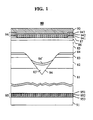
- FIG. 1 schematically depicts an exemplary device according to the invention, namely a channeled substrate buried heterostructure (CSBH) laser diode 80.
- the laser comprises n-InP substrate 81, semi-insulating Fe-doped InP layer 82, n-InP buffer layer 83 and 83', InGaAsP layer 84 and 84' (active layer), p-InP cladding layer 85, and p + InGaAs layer 86.
- the laser further comprises patterned SiO 2 layer 87 defining the p-contact region.
- Numerals 95 and 96 refer to the first and second contact material, respectively.
- Each contact material layer comprises an intermediate layer (941 and 951), Ti layer (942 or 952), and Pt layer (943 or 953).
- Gold layers 90 and 91 complete the p- and n-contact, respectively.
- n-InP (10 18 cm -3 sulfur doped) substrate is grown an epitaxial semi-insulating Fe-doped (resistance greater than 10 6 ⁇ cm) 2 ⁇ m thick InP layer by conventional organometallic vapor phase epitaxy (OMVPE).
- OMVPE organometallic vapor phase epitaxy
- a 0.3 ⁇ m thick SiO 2 layer is formed by plasma deposition, and 2 ⁇ m wide stripe windows opened in the SiO 2 layer by conventional photolithography and etching.
- V-grooves are formed also substantially as described in US patent 4, 595, 454, and the patterned SiO 2 layer is removed by conventional wet etching.
- a double heterostructure consisting of a 1 ⁇ m thick n-InP layer, an InGaAsP layer that is lattice matched to the InP and has a bandgap of 1.3 ⁇ m, a p-InP layer, and a p + InGaAs layer, is then grown by conventional liquid phase epitaxy (LPE) on the grooved surface of the wafer.
- LPE liquid phase epitaxy
- the p-contacts are formed.
- a 300 nm thick layer of SiO 2 is formed on the p-side surface by plasma deposition, and stripes, overlying the V-grooves, are opened in the SiO 2 layer by conventional photolithography and etching.
- a 20 nm thick AuBe layer is deposited, followed by an RTP treatment.
- a 50 nm thick Ti layer, followed by a 75 nm thick Pt layer are deposited by e-gun evaporation, followed by removal of unwanted contact material by conventional lift-off.
- the wafer is then thinned to about 80 ⁇ m by conventional lapping and wet etching. This is followed by formation of the n-contacts, including a 12 nm thick AuGe intermediate layer, in the same manner the p-contacts have been formed previously.
- the wafer is subjected to a RTP treatment, by heating in a forming gas (15% b.v. H 2 ) atmosphere to 440°C for 30 seconds.
Landscapes
- Engineering & Computer Science (AREA)
- Power Engineering (AREA)
- Microelectronics & Electronic Packaging (AREA)
- Computer Hardware Design (AREA)
- Physics & Mathematics (AREA)
- Manufacturing & Machinery (AREA)
- General Physics & Mathematics (AREA)
- Condensed Matter Physics & Semiconductors (AREA)
- Optics & Photonics (AREA)
- Electromagnetism (AREA)
- Ceramic Engineering (AREA)
- Electrodes Of Semiconductors (AREA)
- Led Devices (AREA)
- Semiconductor Lasers (AREA)
Description
- This invention pertains to methods of making semiconductor devices. More particularly, it pertains to methods of making semiconductor devices based on III-V material, exemplarily InP-based photonic and electronic devices, e.g., lasers, LEDs and transistors.
- The need for making a non-rectifying (ohmic) contact to a semiconductor body exists throughout the semiconductor field. In the field of III/V-based semiconductors it has been conventional to use so-called alloyed contacts. For a review of the relevant prior art see applicants' U.S. patent No. 5,036,023, which discloses an advantageous method of making III/V semiconductor devices.
- In particular, the '023 patent discloses depositing p-side Ti/Pt and n-side Ti/Pt onto the relevant surfaces of a semiconductor body, followed by an appropriate heat treatment that results in simultaneous formation of p-side and n-side ohmic contacts. See also A. Katz et al., J. Appl. Physics. Vol 66 (5), p. 2056 (Sept. '89) and EP-A-0 413 491, which report substantially the same subject matter as US-A- 5 036 023.
- JP-A-63095661 discloses a InGaAsP substrate of undisclosed conductivity type with a Au/Ti/Pt/Au layer structure thereon.
- Although the method of the '023 patent is a substantial advance over conventional methods, it would still be desirable to have available a method that can result in higher device yields and/or device lifetime. This application discloses such a method.
- FIG. 1 schematically depicts an exemplary device made according to the invention.
- The invention is as defined by the claims. The invention is a method of making an article that comprises a semiconductor device, exemplarily a semiconductor laser, optical amplifier, or light emitting diode. The method comprises providing a semiconductor body that comprises a p-doped first semiconductor material and an n-doped second semiconductor material. At least the first semiconductor material comprises as major constituents both indium and arsenic. The first and second semiconductor materials form a first and a second surface, respectively, of the semiconductor body. The method further comprises depositing first contact material onto the first surface, heat treating the semiconductor body with the contact material thereon, and carrying out one or more steps towards completion of the article.
- Significantly, the first contact material-depositing step comprises depositing, in sequence, a first intermediate layer that comprises Au (and typically also comprises Be), a first conductor layer that comprises Ti, and a second conductor layer that comprises Pt. The method further comprises depositing, prior to said heat treating step, second contact material onto the second surface, the second contact material comprising third and fourth conductor layers that comprise Ti and Pt, respectively, with the fourth conductor layer being disposed on the third conductor layer. Still furthermore, the heat treating step comprises a "rapid thermal processing" (RTP) step that comprises heating the semiconductor body with the contact material thereon to a temperature in the range 400-500°C for a time in the range 10-100 seconds, such that ohmic contacts to the first and second semiconductor materials are formed simultaneously.
- Currently preferred temperatures and times for processing InP-based devices are in the ranges 425 -475°C and 15-60 seconds, respectively. Appropriate choice of RTP parameters can result in low specific contact resistance,exemplarily 10-7 Ω · cm2 or even lower, for the p-side contact on InGaAs.
- Optionally the inventive process comprises depositing a second intermediate layer (typically comprising Au and Ge) on the second semiconductor surface, followed by deposition of the third and fourth conductor layers. In at least some embodiments the semiconductor body with the first intermediate layer thereon is subjected to a heat treatment (exemplarily RTP) prior to deposition of the other layers.
- The inventive method also comprises a variety of conventional steps, exemplarily including epitaxial deposition of semiconductor layers on a semiconductor substrate, oxide deposition, photolithography, wet and/or dry etching, Au deposition, dicing or cleaving of a semiconductor wafer, AR-coating and mirror deposition, solder bonding and/or wire bonding, and device testing and packaging. Such processing steps require no detailed discussion.
- Although the invention is not so limited, the discussion below will be primarily in terms of devices wherein the first and second surfaces are on opposite sides of the semiconductor body, as is the case in conventional semiconductor lasers and LEDs. In "single side" devices the first and second surfaces are on the same side of the semiconductor body, and the inventive method can be particularly advantageously used to produce such devices as well as III-V-based transistors, as will be apparent to those skilled in the art.
- A significant aspect of the invention is the presence of In and As in at least the first semiconductor material. Typically this material is the "contact layer" of the p-terminal of an inventive device. Exemplarily the contact layer is In1-xGaxAs, with x typically in the range 0. 0.1-0.9, exemplarily 0.47. The presence of both In and As at the metal/semiconductor interface is thought to result in a relatively low Schottky barrier, and thus make possible a contact having a low specific contact resistance.
- In the practice of the inventive method, the semiconductor body can be prepared in conventional manner, and this preparation thus does not require detailed discussion. Furthermore, many of the process steps can be as described in the '023 patent. This pertains, for instance, to the heat treatment after deposition of both contact material layers.
- In embodiments of the inventive process the first and/or third conductor layers are not deposited directly onto the first and/or second semiconductor surfaces but instead are deposited onto a previously deposited Au-containing thin (typically <100 nm) intermediate layer. We have discovered that use of such an intermediate layer in one or both of the contacts frequently results in increased device yield and/or lifetime.
- Exemplarily, the p-side contact comprises a 5-80 nm thick AuBe intermediate layer, and the n-side contact comprises a 7-20 nm thick AuGe intermediate layer. Techniques for depositing AuBe and AuGe layers are well known in the art. Exemplarily, all of the layers of both the first and second contact material can be deposited by means of electron beam evaporation.
- Although embodiments of the inventive method comprise an RTP step subsequent to the deposition of all the conductor layers, some embodiments may comprise an optional heat treatment step (typically also RTP) prior to deposition of any of the conductor layers but subsequent to deposition of the first intermediate layer.
- FIG. 1 schematically depicts an exemplary device according to the invention, namely a channeled substrate buried heterostructure (CSBH)
laser diode 80. The laser comprises n-InP substrate 81, semi-insulating Fe-dopedInP layer 82, n-InP buffer layer 83 and 83', InGaAsPlayer 84 and 84' (active layer), p-InP cladding layer 85, and p+ InGaAs layer 86. The laser further comprises patterned SiO2 layer 87 defining the p-contact region.Numerals Gold layers - Example: A CSBH laser chip as shown in FIG. 1 is produced substantially as follows.
- On a (100)-oriented 275 µm thick, n-InP (1018 cm-3 sulfur doped) substrate is grown an epitaxial semi-insulating Fe-doped (resistance greater than 106 Ω cm) 2 µm thick InP layer by conventional organometallic vapor phase epitaxy (OMVPE). After treating the surface in a manner substantially as described in US patent 4, 595, 454, a 0.3 µm thick SiO2 layer is formed by plasma deposition, and 2 µm wide stripe windows opened in the SiO2 layer by conventional photolithography and etching. Next, V-grooves are formed also substantially as described in US patent 4, 595, 454, and the patterned SiO2 layer is removed by conventional wet etching. A double heterostructure, consisting of a 1 µm thick n-InP layer, an InGaAsP layer that is lattice matched to the InP and has a bandgap of 1.3 µm, a p-InP layer, and a p+ InGaAs layer, is then grown by conventional liquid phase epitaxy (LPE) on the grooved surface of the wafer. After completion of the LPE growth, the p-contacts are formed. In particular, a 300 nm thick layer of SiO2 is formed on the p-side surface by plasma deposition, and stripes, overlying the V-grooves, are opened in the SiO2 layer by conventional photolithography and etching. Subsequently, a 20 nm thick AuBe layer is deposited, followed by an RTP treatment. Next, a 50 nm thick Ti layer, followed by a 75 nm thick Pt layer, are deposited by e-gun evaporation, followed by removal of unwanted contact material by conventional lift-off. The wafer is then thinned to about 80 µm by conventional lapping and wet etching. This is followed by formation of the n-contacts, including a 12 nm thick AuGe intermediate layer, in the same manner the p-contacts have been formed previously. Next the wafer is subjected to a RTP treatment, by heating in a forming gas (15% b.v. H2) atmosphere to 440°C for 30 seconds. This is followed by photolithography and conventional electrodeposition of a 0.8 µm thick gold layer on each of the n- and p-sides of the wafer, to form the n- and p-contact pads, respectively. Next the wafer is scribed and cleaved to form chips with high-quality laser mirror facets, and the thus produced laser chips are tested by conventional means. The metal layers form ohmic contacts, with the p-contacts having a specific contact resistance of less than 10-7 Ω · cm2. The thus produced lasers typically perform as expected, and show good long-term stability.
Claims (6)
- A method of making an article comprising a semiconductor device, the method comprisinga) providing a semiconductor body (80) that comprises a p-doped first semiconductor material (86) comprising both In and As, and that further comprises a n-doped second semiconductor material (81), the first and second semiconductor materials forming a first and a second surface of the body, respectively;b) depositing first contact material (96) onto the first surface and second contact material (95) onto the second surface, with both first and second contact materials comprising, in sequence, a Ti-containing layer (942, 952) and a Pt-containing layer (943, 953);c) heat treating the semiconductor body with the first and second contact materials thereon, the heat treatment comprising heating the semiconductor body with the contact materials thereon to a temperature in the range 400-500°C for a time in the range 10-100 seconds, such that ohmic contacts to the first and second semiconductor materials are formed simultaneously; andd) completing making the article;CHARACTERIZED IN THAT step b) comprises depositing, prior to deposition of the Ti-containing layer (942), a Au-containing layer (941) onto the first surface.
- The method of claim 1, wherein step b) further comprises depositing a Au-containing layer (951) onto the second surface prior to deposition of the Ti-containing layer (952).
- The method of claim 1, additionally comprising heat treating the body with the Au-containing layer (941) on the first surface prior to deposition of the Ti-containing layer (942) thereon.
- The method of claim 3, wherein said additional heat treating prior to deposition of the Ti-containing layer comprises heating the semiconductor body to a temperature in the range 400-500°C for a time in the range 10-100 seconds.
- The method of claim 2, wherein the Au-containing layer (941) on the first surface consists essentially of Au and Be, the Au-containing layer (951) on the second surface consists essentially of Au and Ge, and the Ti-containing and Pt-containing layers consist essentially of Ti and Pt, respectively.
- The method of claim 2, further comprising depositing a Au-containing layer (90, 91) onto each of the Pt-containing layers.
Applications Claiming Priority (2)
| Application Number | Priority Date | Filing Date | Title |
|---|---|---|---|
| US675304 | 1991-03-26 | ||
| US07/675,304 US5100836A (en) | 1989-08-16 | 1991-03-26 | Method of making a semiconductor device |
Publications (3)
| Publication Number | Publication Date |
|---|---|
| EP0508618A2 EP0508618A2 (en) | 1992-10-14 |
| EP0508618A3 EP0508618A3 (en) | 1993-05-05 |
| EP0508618B1 true EP0508618B1 (en) | 1997-09-24 |
Family
ID=24709892
Family Applications (1)
| Application Number | Title | Priority Date | Filing Date |
|---|---|---|---|
| EP92302306A Expired - Lifetime EP0508618B1 (en) | 1991-03-26 | 1992-03-18 | Method of making ohmic contact to a III-V semiconductor device |
Country Status (4)
| Country | Link |
|---|---|
| US (1) | US5100836A (en) |
| EP (1) | EP0508618B1 (en) |
| JP (1) | JP2633434B2 (en) |
| DE (1) | DE69222343T2 (en) |
Family Cites Families (5)
| Publication number | Priority date | Publication date | Assignee | Title |
|---|---|---|---|---|
| US4595454A (en) * | 1984-06-15 | 1986-06-17 | At&T Bell Laboratories | Fabrication of grooved semiconductor devices |
| JPS61150325A (en) * | 1984-12-25 | 1986-07-09 | Fujitsu Ltd | Manufacture of semiconductor device |
| JPS6395661A (en) * | 1986-10-13 | 1988-04-26 | Toshiba Corp | Semiconductor element electrode |
| US5047832A (en) * | 1989-03-10 | 1991-09-10 | Sumitomo Electric Industries, Ltd. | Electrode structure for III-V compound semiconductor element and method of manufacturing the same |
| US5036023A (en) * | 1989-08-16 | 1991-07-30 | At&T Bell Laboratories | Rapid thermal processing method of making a semiconductor device |
-
1991
- 1991-03-26 US US07/675,304 patent/US5100836A/en not_active Expired - Lifetime
-
1992
- 1992-02-03 JP JP4637592A patent/JP2633434B2/en not_active Expired - Lifetime
- 1992-03-18 DE DE69222343T patent/DE69222343T2/en not_active Expired - Fee Related
- 1992-03-18 EP EP92302306A patent/EP0508618B1/en not_active Expired - Lifetime
Also Published As
| Publication number | Publication date |
|---|---|
| JPH04320387A (en) | 1992-11-11 |
| EP0508618A3 (en) | 1993-05-05 |
| DE69222343T2 (en) | 1998-04-09 |
| DE69222343D1 (en) | 1997-10-30 |
| US5100836A (en) | 1992-03-31 |
| JP2633434B2 (en) | 1997-07-23 |
| EP0508618A2 (en) | 1992-10-14 |
Similar Documents
| Publication | Publication Date | Title |
|---|---|---|
| EP0413491B1 (en) | Method of making a semiconductor device | |
| KR100649777B1 (en) | INxALyGAzN OPTICAL EMITTERS FABRICATED VIA SUBSTRATE REMOVAL | |
| EP0390262B1 (en) | Radiation-emitting semiconductor device and method of manufacturing such a semiconductor device | |
| US5985687A (en) | Method for making cleaved facets for lasers fabricated with gallium nitride and other noncubic materials | |
| US8193016B2 (en) | Semiconductor laser device and method of manufacturing the same | |
| US5208821A (en) | Buried heterostructure lasers using MOCVD growth over patterned substrates | |
| US8306086B2 (en) | Algainn-based lasers produced using etched facet technology | |
| US20210408767A1 (en) | O-band silicon-based high-speed semiconductor laser diode for optical communication and its manufacturing method | |
| US4441187A (en) | A semiconductor laser light source | |
| US20120228664A1 (en) | Nitride semiconductor light emitting device and method of manufacturing the same | |
| US4725112A (en) | Buried undercut mesa-like waveguide | |
| US5793788A (en) | Semiconductor light emitting element with p-type non-alloy electrode including a platinum layer and method for fabricating the same | |
| EP0508618B1 (en) | Method of making ohmic contact to a III-V semiconductor device | |
| EP0312401B1 (en) | Semiconductor devices and method of manufacturing the same | |
| US5721751A (en) | Semiconductor laser | |
| US5887011A (en) | Semiconductor laser | |
| US5323412A (en) | Semiconductor laser device | |
| JP3665911B2 (en) | Semiconductor optical device manufacturing method and semiconductor optical device | |
| CN114006265B (en) | Vertical cavity surface emitting laser and manufacturing method thereof | |
| JP3451818B2 (en) | Semiconductor laser | |
| JPS63129687A (en) | Semiconductor laser and manufacture thereof | |
| JPH01239984A (en) | Semiconductor laser diode and its manufacture | |
| JPS6316689A (en) | Semiconductor device | |
| JPH0750267A (en) | Growth method of ii-vi compound semiconductor | |
| JPS61113289A (en) | Manufacture of semiconductor light emitting diode |
Legal Events
| Date | Code | Title | Description |
|---|---|---|---|
| PUAI | Public reference made under article 153(3) epc to a published international application that has entered the european phase |
Free format text: ORIGINAL CODE: 0009012 |
|
| AK | Designated contracting states |
Kind code of ref document: A2 Designated state(s): DE FR GB |
|
| PUAL | Search report despatched |
Free format text: ORIGINAL CODE: 0009013 |
|
| AK | Designated contracting states |
Kind code of ref document: A3 Designated state(s): DE FR GB |
|
| 17P | Request for examination filed |
Effective date: 19931021 |
|
| RAP3 | Party data changed (applicant data changed or rights of an application transferred) |
Owner name: AT&T CORP. |
|
| 17Q | First examination report despatched |
Effective date: 19951030 |
|
| GRAG | Despatch of communication of intention to grant |
Free format text: ORIGINAL CODE: EPIDOS AGRA |
|
| GRAH | Despatch of communication of intention to grant a patent |
Free format text: ORIGINAL CODE: EPIDOS IGRA |
|
| GRAH | Despatch of communication of intention to grant a patent |
Free format text: ORIGINAL CODE: EPIDOS IGRA |
|
| GRAA | (expected) grant |
Free format text: ORIGINAL CODE: 0009210 |
|
| AK | Designated contracting states |
Kind code of ref document: B1 Designated state(s): DE FR GB |
|
| REF | Corresponds to: |
Ref document number: 69222343 Country of ref document: DE Date of ref document: 19971030 |
|
| ET | Fr: translation filed | ||
| PLBE | No opposition filed within time limit |
Free format text: ORIGINAL CODE: 0009261 |
|
| STAA | Information on the status of an ep patent application or granted ep patent |
Free format text: STATUS: NO OPPOSITION FILED WITHIN TIME LIMIT |
|
| 26N | No opposition filed | ||
| PGFP | Annual fee paid to national office [announced via postgrant information from national office to epo] |
Ref country code: FR Payment date: 20010222 Year of fee payment: 10 |
|
| PGFP | Annual fee paid to national office [announced via postgrant information from national office to epo] |
Ref country code: DE Payment date: 20010330 Year of fee payment: 10 |
|
| REG | Reference to a national code |
Ref country code: GB Ref legal event code: IF02 |
|
| PG25 | Lapsed in a contracting state [announced via postgrant information from national office to epo] |
Ref country code: DE Free format text: LAPSE BECAUSE OF NON-PAYMENT OF DUE FEES Effective date: 20021001 |
|
| PG25 | Lapsed in a contracting state [announced via postgrant information from national office to epo] |
Ref country code: FR Free format text: LAPSE BECAUSE OF NON-PAYMENT OF DUE FEES Effective date: 20021129 |
|
| REG | Reference to a national code |
Ref country code: FR Ref legal event code: ST |
|
| PGFP | Annual fee paid to national office [announced via postgrant information from national office to epo] |
Ref country code: GB Payment date: 20110321 Year of fee payment: 20 |
|
| REG | Reference to a national code |
Ref country code: GB Ref legal event code: PE20 Expiry date: 20120317 |
|
| PG25 | Lapsed in a contracting state [announced via postgrant information from national office to epo] |
Ref country code: GB Free format text: LAPSE BECAUSE OF EXPIRATION OF PROTECTION Effective date: 20120317 |