EP0507346A2 - Vorrichtung zur Verbesserung der Kontouren eines Bildsignals - Google Patents
Vorrichtung zur Verbesserung der Kontouren eines Bildsignals Download PDFInfo
- Publication number
- EP0507346A2 EP0507346A2 EP92105880A EP92105880A EP0507346A2 EP 0507346 A2 EP0507346 A2 EP 0507346A2 EP 92105880 A EP92105880 A EP 92105880A EP 92105880 A EP92105880 A EP 92105880A EP 0507346 A2 EP0507346 A2 EP 0507346A2
- Authority
- EP
- European Patent Office
- Prior art keywords
- digital data
- signal
- image signal
- sampled digital
- delayed
- Prior art date
- Legal status (The legal status is an assumption and is not a legal conclusion. Google has not performed a legal analysis and makes no representation as to the accuracy of the status listed.)
- Granted
Links
Images


Classifications
-
- H—ELECTRICITY
- H04—ELECTRIC COMMUNICATION TECHNIQUE
- H04N—PICTORIAL COMMUNICATION, e.g. TELEVISION
- H04N5/00—Details of television systems
- H04N5/14—Picture signal circuitry for video frequency region
- H04N5/20—Circuitry for controlling amplitude response
- H04N5/205—Circuitry for controlling amplitude response for correcting amplitude versus frequency characteristic
- H04N5/208—Circuitry for controlling amplitude response for correcting amplitude versus frequency characteristic for compensating for attenuation of high frequency components, e.g. crispening, aperture distortion correction
Definitions
- the present invention relates to a visual image reproducing device for use such as in a television receiver, a videotape recorder or a video projector and, more particularly, to an image signal outline enhancing device which can be used to enhance the outline of such an image signal having a very high frequency as a color difference signal, for a sharper image reproduction.
- the image signal outline enhancing devices have become increasingly important as a means for sharpening the image reproduced on the CRT screen by enhancing the leading and trailing edges of such an image signal having a very high frequency as a color difference signals.
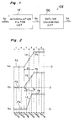
- Fig. 7 and Figs. 8 and 9 are, respectively, a block diagram and graphs showing the input/output relationship in an example of a conventional image signal outline enhancing device.
- the outline enhancing device CEp includes a rise time detecting circuit 11 which detects the rise time tr required for the color difference signal Sa to rise from the zero level to its steady peak amplitude level, a correction pulse generation circuit 12 for generating a correction pulse Sc for the same period as the detected rise time tr, and a hold circuit 13 for keeping the output signal Se' at the zero level during the correction pulse Sc is generated.
- a color difference signal enhancing device CEp thus constructed operates as described below, with references to Figs. 8 and 9.
- the rise time detecting circuit 11 detects the rise time tr which is the period from a time when the when the color difference signal Sa starts to rise to a time when the signal Sa exceeds the threshold level Vt.
- the correction pulse generation circuit 12 produces the correction pulse Sc for the period tr.
- the hold circuit 13 holds the output signal Se' at the zero level. After the period tr, the hold circuit enables the output signal Se' to rise. As a result, the output signal Se' rapidly rises to the steady level with a greater gradient than that of the difference signal Sa.
- the rise time detecting circuit 11 can not detect the rise time tr correctly.
- the color difference signal Sa makes small, rapid variations in a waveform caused by mechanical vibrations, fluctuations in supply voltage, control-system instability, and other causes, the signal Sa also fluctuates or jitters.
- the waveform fluctuates up, the color difference signal Sa shifts to a position above the threshold level Vt as indicated in an imaginary line Sau.
- the signal Sa shifts to a position below the threshold level Vt as indicated in an imaginary line Sad.
- the correction pulse generation circuit 12 also alternatively produces or does not produce the correction pulse Sc, accordingly. Therefore, the produced output signal Se' alternatively shows a non-corrected waveform Se'n and a corrected waveform Se'c as shown Fig. 8, causing the signal Se' to jitter, too.
- the present invention has been developed with a view to substantially solving the above described disadvantages and has for its essential object to provide an improved image signal outline enhancing device.
- an image signal outline enhancing device for enhancing an outline of image formed by an image signal having leading and trailing-edge portions and a pulse portion between the leading and trailing-edge portions comprising an interpolating means for estimating a digital data between subsequent two of the sampled digital data and for inserting the estimated digital data and an outline enhancing means for enhancing the image signal by making the leading and trailing-edge portions steeper.
- a block diagram of a color difference signal enhancing device CE receives a color difference signal Sa in digital form sampled in a predetermined interval t.
- a color difference signal Sa in digital form sampled in a predetermined interval t.
- each of small circles represents a sampled digital data of the color difference signal Sa which has a leading-edge portion Lp, a pulse portion Pp, and a trailing-edge portion (not shown).
- the color difference signal enhancing device CE comprises an interpolation filter circuit IF which interpolates the color difference signal by inserting estimated digital data between two subsequent sampled digital data of the color difference signal Sa and produces an interpolated signal Sb.
- the interpolated signal Sb also has a leading-edge portion Lb, a pulse portion Pb, and a trailing-edge portion (not shown).
- signal Sb has a greater number of digital data per unit time, resulting in closer interval of digital data.
- the device CE further comprises an outline enhancing circuit OC which produces an outline enhanced signal Se based on the interpolated signal Sb.
- the outline enhanced signal Se also has a leading-edge portion Le, a pulse portion Pe, and a trailing-edge portion (no shown).
- signal Se has edge potions, e.g., Le, slanted at a greater gradient.
- FIG. 2 A color-bar test pattern image in which a blue bar and a red bar are closely placed is considered.
- a color difference signal Sa of a line scanned across this color bar image is partially shown in Fig. 2, wherein a flat portion Fp before the leading-edge portion Lp represents a blue bar, a leading-edge portion Lp represents a boarder between the blue and red bars.
- signal Sa has a leading-edge portion Lp which continues for two sampling periods, whereas signal Se has is one sampling period.
- the color difference signal Sa is shown as a positive going signal in this embodiment, the present invention is applicable also to a negative going signal.
- the interpolation filer circuit IF estimates a digital data which is inserted between two subsequent digital data the color difference signal Sa, as indicated by a small triangle.
- the interpolation filter circuit IF produces the interpolated signal Sb.
- the interpolated signal Sb has digital data occurring twice as much as that in the signal Sa, meaning that the digital data occurring interval is 1/2t.
- the outline enhancing circuit OC produces the enhanced signal Se based on the interpolated signal Sb such that the gradient of the leading-edge portion Le is made steeper than that of the signal Sb. In other wards, the leading-edge portion Le of the signal Se occupies only a period t, whereas the leading edge portion Lb of signal Sb occupies a period 2t. Thus, the signal Se rises in a half period of that of the color difference signal Sa, resulting in enhancement of the outline.
- the details of the outline enhancing circuit OC is disclosed in the prior E.P. patent application No. 92 105 092.8 filed March 25, 1992 by the same applicants as the present application.
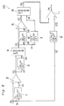
- the interpolation filer circuit IF comprises a firs flip-flop circuit 1 which latches the color difference signal Sa in response to a leading-edge of a clock signal Pa and produces a delayed color difference signal Sa' which is delayed by a period t.
- a second flip-flop circuit 2 latches the signal Sa' in response to the clock signal Pa and produces a firs delayed color difference signal Sd1 which is delayed by a period t.
- An adder 3 adds the signal Sa' to the signal Sd1 and produces a first intermediate signal Si1.
- a multiplier 4 multiplies the first intermediate signal Si1 by 1/2 and produces a second intermediate signal Si2 which is equal to an average between two subsequent sampled digital data.
- a third flip-flop circuit 5 latches the signal Si2 in response to the clock signal Pa, and produces a second latched color difference signal Sl.
- a third flip-flop circuit 6 latches the first signal Sd1 and produces a second delayed color difference signal Sd2.
- a selector 7 selects the signal Sl when the signal Pa is 0 (low) and the signal Sd2 when the signal Pa is 1 (high), and produces a third intermediate signal Si3.
- a fifth flip-flop circuit 8 latches the third intermediate signal Si3 in response to a system clock signal Ps and produces the interpolated signal Sb.
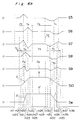
- the outline enhancing circuit OC operates as follows.
- a first delay circuit 1 (Fig. 5) delays the interpolated signal Sb (Fig. 6a) by a first delay period t1 and produces a delayed interpolated signal S2 (Fig. 6a).
- a first subtracter 2 (Fig. 5) subtracts the signal S2 from the signal Sb and produces a primary differentiated signal S3 (Fig. 6a).
- a second delay circuit 3 (Fig. 5) delays the signal S3 by a first delay period t1 and produces a delayed primary differentiated signal S4 (Fig. 6a).
- a first minimum circuit 4 (Fig. 5) selects either of signals S3 and S4 whose absolute amplitude is smaller than the other and produces a minimum primary differentiated signal S5 (Fig. 6a).
- a third delay circuit 5 delays the signal S5 by a second delay period t2 and produces a first delayed minimum primary differentiated signal S6 (Fig. 6b).
- a second subtracter 6 subtracts the signal S6 from the signal S5 and produces a second differentiated signal S7 (Fig. 6b).
- a fourth delay circuit 7 delays the signal S5 by the second delay period of t2/2 and produces a second delayed minimum primary differentiated signal S8 (Fig. 6b).
- a second minimum circuit 8 (Fig.
- the fifth delay circuit 9 (Fig. 5) delays the interpolated signal Sb by a period of t1+t2/2 and produces a second delayed interpolated signal S10 (Fig. 6b) which is synchronized with the signal S9.
- a third subtracter 11 (fig. 5) subtracts the signal S9 from the signal S10 and produces an output signal Se.
- the signal Se has the leading and railing edges which are more steep than those of the interpolated signal Sb, as shown.
- the outline enhancing circuit OC does no compare the amplitude of the color difference signal Sa with the predetermined threshold V, the circuit OC can enhance the outline of the signal Sa stably and correctly under no influence of the jittering of the color difference signal Sa.
- the interpolation filter circuit IF is provided before the outline enhancing circuit OC to provide an estimated digital data between two subsequent sampled digital data.
- the color difference signal enhancing device CE of the preferred embodiment of present invention it is possible to enhance the outline of any level of color difference signal such that the interpolation filer circuit IF interpolates and increases the digital data within the sampling interval of the signal and that the outline enhancing circuit OC improves the steepness of the leading and railing edges of the signal based on the interpolated digital data.
Landscapes
- Engineering & Computer Science (AREA)
- Multimedia (AREA)
- Signal Processing (AREA)
- Processing Of Color Television Signals (AREA)
- Picture Signal Circuits (AREA)
Applications Claiming Priority (2)
| Application Number | Priority Date | Filing Date | Title |
|---|---|---|---|
| JP3071523A JPH04306976A (ja) | 1991-04-04 | 1991-04-04 | 色信号輪郭補正装置 |
| JP71523/91 | 1991-04-04 |
Publications (3)
| Publication Number | Publication Date |
|---|---|
| EP0507346A2 true EP0507346A2 (de) | 1992-10-07 |
| EP0507346A3 EP0507346A3 (en) | 1993-06-09 |
| EP0507346B1 EP0507346B1 (de) | 1996-09-04 |
Family
ID=13463173
Family Applications (1)
| Application Number | Title | Priority Date | Filing Date |
|---|---|---|---|
| EP92105880A Expired - Lifetime EP0507346B1 (de) | 1991-04-04 | 1992-04-06 | Vorrichtung zur Verbesserung der Kontouren eines Bildsignals |
Country Status (4)
| Country | Link |
|---|---|
| EP (1) | EP0507346B1 (de) |
| JP (1) | JPH04306976A (de) |
| CA (1) | CA2065069C (de) |
| DE (1) | DE69213289T2 (de) |
Family Cites Families (4)
| Publication number | Priority date | Publication date | Assignee | Title |
|---|---|---|---|---|
| CA1311297C (en) * | 1986-09-30 | 1992-12-08 | Theodore Stanley Rzeszewski | Video signal enhancement by adaptive digital signal processing |
| JP2672541B2 (ja) * | 1988-01-11 | 1997-11-05 | キヤノン株式会社 | 画像処理装置 |
| GB8822161D0 (en) * | 1988-09-21 | 1988-10-26 | Abekas Video Systems | Video signal processing |
| JPH0326067A (ja) * | 1989-06-22 | 1991-02-04 | Toshiba Corp | カラー画像読取装置 |
-
1991
- 1991-04-04 JP JP3071523A patent/JPH04306976A/ja active Pending
-
1992
- 1992-04-03 CA CA002065069A patent/CA2065069C/en not_active Expired - Fee Related
- 1992-04-06 DE DE69213289T patent/DE69213289T2/de not_active Expired - Fee Related
- 1992-04-06 EP EP92105880A patent/EP0507346B1/de not_active Expired - Lifetime
Also Published As
| Publication number | Publication date |
|---|---|
| EP0507346A3 (en) | 1993-06-09 |
| DE69213289T2 (de) | 1997-04-24 |
| JPH04306976A (ja) | 1992-10-29 |
| EP0507346B1 (de) | 1996-09-04 |
| DE69213289D1 (de) | 1996-10-10 |
| CA2065069A1 (en) | 1992-10-05 |
| CA2065069C (en) | 1998-01-27 |
Similar Documents
| Publication | Publication Date | Title |
|---|---|---|
| EP0302500B1 (de) | Schaltung zur Verarbeitung eines Farbdifferenzsignals unter Verwendung der Änderung eines Luminanzsignals | |
| JP2814039B2 (ja) | クランプ回路 | |
| US5029004A (en) | Edge enhancement apparatus useful with liquid crystal displays | |
| EP0211570B1 (de) | Anzeigesystem per Zeilenfolgeverfahren mit Korrektur für ungenormte Signale | |
| EP0447210B1 (de) | FM-Modulator mit Trägerrücksetzung und Verfahren zum Frequenzmodulieren eines Videosignals | |
| KR100274527B1 (ko) | 동기화 회로 | |
| JPH0620280B2 (ja) | テレビジョン信号用振幅検出回路 | |
| KR920009012B1 (ko) | 자동주파수 제어회로 | |
| KR100466553B1 (ko) | 지연 정정 회로 | |
| EP0507346B1 (de) | Vorrichtung zur Verbesserung der Kontouren eines Bildsignals | |
| US6801706B1 (en) | Jitter correcting apparatus and method for video signals | |
| GB2056823A (en) | Line scan circuit for crt display | |
| EP0574200A1 (de) | Digitale Modulationseinrichtung für Chrominanzsignale | |
| JP3519878B2 (ja) | 垂直同期動作の制御回路 | |
| US5258841A (en) | Horizontal synchronizing signal separation circuit | |
| KR940004511B1 (ko) | 브이씨알의 재생 색신호 자동 보정 시스템 | |
| JP3014791B2 (ja) | 垂直同期信号正規化装置 | |
| JP2675441B2 (ja) | 磁気記録再生装置 | |
| JP3385646B2 (ja) | 画像処理回路 | |
| JP2507325B2 (ja) | テレビジョン信号処理装置 | |
| JP3077154B2 (ja) | エンハンサ回路 | |
| JP2000152031A (ja) | 信号クランプ装置および記録媒体 | |
| JPS59219089A (ja) | 磁気記録再生回路のカラ−プロセス回路 | |
| JPH04369179A (ja) | 輪郭補正装置 | |
| JPH0563068B2 (de) |
Legal Events
| Date | Code | Title | Description |
|---|---|---|---|
| PUAI | Public reference made under article 153(3) epc to a published international application that has entered the european phase |
Free format text: ORIGINAL CODE: 0009012 |
|
| 17P | Request for examination filed |
Effective date: 19920406 |
|
| AK | Designated contracting states |
Kind code of ref document: A2 Designated state(s): DE FR GB IT |
|
| PUAL | Search report despatched |
Free format text: ORIGINAL CODE: 0009013 |
|
| AK | Designated contracting states |
Kind code of ref document: A3 Designated state(s): DE FR GB IT |
|
| 17Q | First examination report despatched |
Effective date: 19940113 |
|
| GRAH | Despatch of communication of intention to grant a patent |
Free format text: ORIGINAL CODE: EPIDOS IGRA |
|
| GRAH | Despatch of communication of intention to grant a patent |
Free format text: ORIGINAL CODE: EPIDOS IGRA |
|
| GRAA | (expected) grant |
Free format text: ORIGINAL CODE: 0009210 |
|
| AK | Designated contracting states |
Kind code of ref document: B1 Designated state(s): DE FR GB IT |
|
| ET | Fr: translation filed | ||
| REF | Corresponds to: |
Ref document number: 69213289 Country of ref document: DE Date of ref document: 19961010 |
|
| ITF | It: translation for a ep patent filed | ||
| PLBE | No opposition filed within time limit |
Free format text: ORIGINAL CODE: 0009261 |
|
| STAA | Information on the status of an ep patent application or granted ep patent |
Free format text: STATUS: NO OPPOSITION FILED WITHIN TIME LIMIT |
|
| 26N | No opposition filed | ||
| REG | Reference to a national code |
Ref country code: GB Ref legal event code: IF02 |
|
| PGFP | Annual fee paid to national office [announced via postgrant information from national office to epo] |
Ref country code: IT Payment date: 20090424 Year of fee payment: 18 Ref country code: FR Payment date: 20090417 Year of fee payment: 18 Ref country code: DE Payment date: 20090402 Year of fee payment: 18 |
|
| PGFP | Annual fee paid to national office [announced via postgrant information from national office to epo] |
Ref country code: GB Payment date: 20090401 Year of fee payment: 18 |
|
| GBPC | Gb: european patent ceased through non-payment of renewal fee |
Effective date: 20100406 |
|
| REG | Reference to a national code |
Ref country code: FR Ref legal event code: ST Effective date: 20101230 |
|
| PG25 | Lapsed in a contracting state [announced via postgrant information from national office to epo] |
Ref country code: DE Free format text: LAPSE BECAUSE OF NON-PAYMENT OF DUE FEES Effective date: 20101103 |
|
| PG25 | Lapsed in a contracting state [announced via postgrant information from national office to epo] |
Ref country code: IT Free format text: LAPSE BECAUSE OF NON-PAYMENT OF DUE FEES Effective date: 20100406 Ref country code: GB Free format text: LAPSE BECAUSE OF NON-PAYMENT OF DUE FEES Effective date: 20100406 |
|
| PG25 | Lapsed in a contracting state [announced via postgrant information from national office to epo] |
Ref country code: FR Free format text: LAPSE BECAUSE OF NON-PAYMENT OF DUE FEES Effective date: 20100430 |