EP0505130A2 - Verdünnte ladungsgekoppelte Anordnungen und deren Herstellungsverfahren - Google Patents
Verdünnte ladungsgekoppelte Anordnungen und deren Herstellungsverfahren Download PDFInfo
- Publication number
- EP0505130A2 EP0505130A2 EP92302254A EP92302254A EP0505130A2 EP 0505130 A2 EP0505130 A2 EP 0505130A2 EP 92302254 A EP92302254 A EP 92302254A EP 92302254 A EP92302254 A EP 92302254A EP 0505130 A2 EP0505130 A2 EP 0505130A2
- Authority
- EP
- European Patent Office
- Prior art keywords
- charge
- coupled device
- thinned
- silicon
- coupled
- Prior art date
- Legal status (The legal status is an assumption and is not a legal conclusion. Google has not performed a legal analysis and makes no representation as to the accuracy of the status listed.)
- Ceased
Links
Images

Classifications
-
- H—ELECTRICITY
- H10—SEMICONDUCTOR DEVICES; ELECTRIC SOLID-STATE DEVICES NOT OTHERWISE PROVIDED FOR
- H10F—INORGANIC SEMICONDUCTOR DEVICES SENSITIVE TO INFRARED RADIATION, LIGHT, ELECTROMAGNETIC RADIATION OF SHORTER WAVELENGTH OR CORPUSCULAR RADIATION
- H10F39/00—Integrated devices, or assemblies of multiple devices, comprising at least one element covered by group H10F30/00, e.g. radiation detectors comprising photodiode arrays
- H10F39/011—Manufacture or treatment of image sensors covered by group H10F39/12
- H10F39/026—Wafer-level processing
-
- H—ELECTRICITY
- H10—SEMICONDUCTOR DEVICES; ELECTRIC SOLID-STATE DEVICES NOT OTHERWISE PROVIDED FOR
- H10P—GENERIC PROCESSES OR APPARATUS FOR THE MANUFACTURE OR TREATMENT OF DEVICES COVERED BY CLASS H10
- H10P52/00—Grinding, lapping or polishing of wafers, substrates or parts of devices
- H10P52/40—Chemomechanical polishing [CMP]
- H10P52/402—Chemomechanical polishing [CMP] of semiconductor materials
-
- H—ELECTRICITY
- H10—SEMICONDUCTOR DEVICES; ELECTRIC SOLID-STATE DEVICES NOT OTHERWISE PROVIDED FOR
- H10F—INORGANIC SEMICONDUCTOR DEVICES SENSITIVE TO INFRARED RADIATION, LIGHT, ELECTROMAGNETIC RADIATION OF SHORTER WAVELENGTH OR CORPUSCULAR RADIATION
- H10F30/00—Individual radiation-sensitive semiconductor devices in which radiation controls the flow of current through the devices, e.g. photodetectors
- H10F30/20—Individual radiation-sensitive semiconductor devices in which radiation controls the flow of current through the devices, e.g. photodetectors the devices having potential barriers, e.g. phototransistors
- H10F30/21—Individual radiation-sensitive semiconductor devices in which radiation controls the flow of current through the devices, e.g. photodetectors the devices having potential barriers, e.g. phototransistors the devices being sensitive to infrared, visible or ultraviolet radiation
- H10F30/28—Individual radiation-sensitive semiconductor devices in which radiation controls the flow of current through the devices, e.g. photodetectors the devices having potential barriers, e.g. phototransistors the devices being sensitive to infrared, visible or ultraviolet radiation the devices being characterised by field-effect operation, e.g. junction field-effect phototransistors
- H10F30/2823—Individual radiation-sensitive semiconductor devices in which radiation controls the flow of current through the devices, e.g. photodetectors the devices having potential barriers, e.g. phototransistors the devices being sensitive to infrared, visible or ultraviolet radiation the devices being characterised by field-effect operation, e.g. junction field-effect phototransistors the devices being conductor-insulator-semiconductor devices, e.g. diodes or charge-coupled devices [CCD]
-
- H—ELECTRICITY
- H10—SEMICONDUCTOR DEVICES; ELECTRIC SOLID-STATE DEVICES NOT OTHERWISE PROVIDED FOR
- H10F—INORGANIC SEMICONDUCTOR DEVICES SENSITIVE TO INFRARED RADIATION, LIGHT, ELECTROMAGNETIC RADIATION OF SHORTER WAVELENGTH OR CORPUSCULAR RADIATION
- H10F39/00—Integrated devices, or assemblies of multiple devices, comprising at least one element covered by group H10F30/00, e.g. radiation detectors comprising photodiode arrays
- H10F39/80—Constructional details of image sensors
-
- H—ELECTRICITY
- H10—SEMICONDUCTOR DEVICES; ELECTRIC SOLID-STATE DEVICES NOT OTHERWISE PROVIDED FOR
- H10P—GENERIC PROCESSES OR APPARATUS FOR THE MANUFACTURE OR TREATMENT OF DEVICES COVERED BY CLASS H10
- H10P50/00—Etching of wafers, substrates or parts of devices
- H10P50/60—Wet etching
- H10P50/64—Wet etching of semiconductor materials
- H10P50/642—Chemical etching
-
- Y—GENERAL TAGGING OF NEW TECHNOLOGICAL DEVELOPMENTS; GENERAL TAGGING OF CROSS-SECTIONAL TECHNOLOGIES SPANNING OVER SEVERAL SECTIONS OF THE IPC; TECHNICAL SUBJECTS COVERED BY FORMER USPC CROSS-REFERENCE ART COLLECTIONS [XRACs] AND DIGESTS
- Y10—TECHNICAL SUBJECTS COVERED BY FORMER USPC
- Y10S—TECHNICAL SUBJECTS COVERED BY FORMER USPC CROSS-REFERENCE ART COLLECTIONS [XRACs] AND DIGESTS
- Y10S148/00—Metal treatment
- Y10S148/012—Bonding, e.g. electrostatic for strain gauges
-
- Y—GENERAL TAGGING OF NEW TECHNOLOGICAL DEVELOPMENTS; GENERAL TAGGING OF CROSS-SECTIONAL TECHNOLOGIES SPANNING OVER SEVERAL SECTIONS OF THE IPC; TECHNICAL SUBJECTS COVERED BY FORMER USPC CROSS-REFERENCE ART COLLECTIONS [XRACs] AND DIGESTS
- Y10—TECHNICAL SUBJECTS COVERED BY FORMER USPC
- Y10S—TECHNICAL SUBJECTS COVERED BY FORMER USPC CROSS-REFERENCE ART COLLECTIONS [XRACs] AND DIGESTS
- Y10S148/00—Metal treatment
- Y10S148/135—Removal of substrate
-
- Y—GENERAL TAGGING OF NEW TECHNOLOGICAL DEVELOPMENTS; GENERAL TAGGING OF CROSS-SECTIONAL TECHNOLOGIES SPANNING OVER SEVERAL SECTIONS OF THE IPC; TECHNICAL SUBJECTS COVERED BY FORMER USPC CROSS-REFERENCE ART COLLECTIONS [XRACs] AND DIGESTS
- Y10—TECHNICAL SUBJECTS COVERED BY FORMER USPC
- Y10S—TECHNICAL SUBJECTS COVERED BY FORMER USPC CROSS-REFERENCE ART COLLECTIONS [XRACs] AND DIGESTS
- Y10S438/00—Semiconductor device manufacturing: process
- Y10S438/977—Thinning or removal of substrate
Definitions
- the present invention relates to charge-coupled devices and in particular, such devices which are thinned to allow illumination of the backside of the device to improve quantum efficiency and UV spectral response.
- the invention is particularly directed towards an improved method for thinning such charge-coupled devices.
- Charge-coupled devices are typically made of silicon and are used as solid-state imagers by taking advantage of the properties of a silicon crystal lattice. In the crystalline form, each atom of silicon is covalently bonded to its neighbor. Energy greater than the energy gap of about 1.1 eV is required to break a bond and create an electron hole pair. Incident electromagnetic radiation in the form of photons of wavelength shorter than 1 um can break the bonds and generate electron hole pairs.
- the wavelength of incoming light and the photon absorption depth are directly related, the shorter the wavelength, the shorter the penetration depth into the silicon.
- Silicon becomes transparent at a wavelength of approximately 1100 nm and is essentially opaque to light at wavelengths shorter than 400 nm.
- High energy particles, X-rays and cosmic rays can break many thousands of bonds; therefore, excessive exposure can cause damage to the crystal lattice. Bonds can also be broken by thermal agitation. At room temperature, approximately 50 bonds per second per um3 are broken and recombined on a continuous basis. The rate of electron hole pair generation due to thermal energy is highly temperature-dependent and can be reduced arbitrarily through cooling.
- the potential well concept was developed, wherein a thin layer of silicon dioxide is grown on a section of silicon, and a conductive gate structure is applied over the oxide.
- the gate structure is formed in an array of columns and rows, thus making it possible by applying a positive electrical potential to various gate elements to create depletion regions where free electrons generated by the incoming photons can be stored.
- the depletion region, or well, containing the free electrons can be caused to migrate along a column or row, so that the signal may eventually be output at the edge of the array.
- the gate structure is arranged with multiple phases, particularly three phases, so that the potential wells may be easily migrated through the silicon to an output device.
- the charge transfer efficiency of a charge-coupled device is most important, as is the quantum efficiency and the spectral response. These considerations are particularly important when extremely low light levels are to be sensed.
- the gates are usually made of very thin polysilicon, which is reasonably transparent to long wavelengths but becomes opaque at wavelengths shorter than 400 nm. Thus, at short wavelengths, the gate structure attenuates incoming light.
- Figure 1A illustrates schematically a cross-section of a typical thick-bodied charge-coupled device.
- the device includes a silicon body 2, a silicon dioxide layer 4 and a gate array 6 formed on the silicon dioxide layer.
- Incoming light is illustrated by arrows 8 as illuminating a front side of the silicon 2.
- Figure 1B illustrates a cross-section of a thinned charge-coupled device with light illuminating a backside.
- the thinned charge-coupled device having a thickness of approximately 10 um, has improved quantum efficiency and UV spectral response.
- Potassium hydroxide is an anisotropic etchant and therefore only etches the silicon directly behind the pixels, which results in a rectangular membrane attached to a rectangular hoop of silicon, as illustrated in Figure 1B.
- This structure does not require mechanical support for thinning; however, it results in a somewhat buckled, non-planar charge-coupled device silicon membrane.
- the chemical etchants are extremely strong and have varying reaction rates, thereby making it difficult to control the rate of etching, resulting in very poor yields.
- the techniques used for wet etching with the chemical etchants required that the pixel face of the charge-coupled device be protected during the chemical etching; typically, the pixel face of the charge-coupled device is waxed to a support substrate, while the back is etched. Thereafter, the charge-coupled device is transferred to a second, optically-transparent, substrate to provide proper support.
- This technique has two major drawbacks. Firstly, the excessive handling required significantly increases the possibility of damaging the charge-coupled device. Secondly, the backside of the charge-coupled device, which is mounted to an optically-transparent substrate, has two layers through which light must pass under normal use, thereby causing additional attenuation.
- the present invention contemplates a method for thinning a charge-coupled device, which method overcomes the drawbacks of the prior art.
- a standard thick silicon charge-coupled device has its pixel face mounted to a transparent glass substrate, which has a thermal coefficient of expansion matched to the charge-coupled device. This bonding is accomplished using a thin layer of thermoset epoxy.
- the backside silicon of the charge-coupled device is thinned to 10 ⁇ .5 um using a two-step chemi-mechanical process.
- the bulk silicon is thinned to 75 um with a 700 micro-grit aluminum oxide abrasive and is then thinned and polished to 10 um using 80 nm grit colloidal silica.
- Access from the backside to the aluminum bonding pads of the device is achieved by photolithographic patterning and reactive ion etching of the silicon above the bonding pads.
- the charge-coupled device is then packaged and wire-bonded in a structure which offers support for the thin silicon/glass sandwich structure and allows for unobstructed backside illumination.
- the thinned silicon membrane is secured to a rigid, flat, smooth glass substrate for proper support.
- the polishing step results in a specular, optically smooth surface devoid of surface damage or defects.
- the thinned backside silicon has no overlying structure to attenuate or distort the incoming light during normal charge-coupled device use.
- the packaging of the resulting charge-coupled device is straightforward, since the aluminum bonding pads are facing the package opening, in a manner similar to the situation when the gate side of the device is illuminated.
- di primary objective of the present invention is to provide a method of thinning charge-coupled devices which results in improved device yield and provides a flatness of ⁇ /2 or better.
- Another objective of the present invention is to provide a thinned charge-coupled device wherein the backside may be directly illuminated without the requirement for the illumination to pass through additional supporting structures.
- Another objective of the present invention is to provide a thinned charge-coupled device which is adapted to be easily mounted in a typical charge-coupled device package.
- Figures 1A and 1B are cross-section illustrations of thick and thinned charge-coupled devices, respectively.
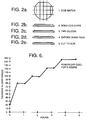
- FIG. 2 illustrates the basic steps of the present invention.
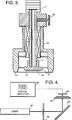
- Figure 3 schematically illustrates a fixture used in the present invention for lapping and polishing.
- Figure 4 illustrates a thickness measuring technique used to measure the final thickness of the thinned charge-coupled device.
- Figure 5 is a partial cross-section of a thinned charge-coupled device with the aluminum bonding pads exposed.
- Figure 6 is a time-temperature schedule for the curing of the epoxy which bonds the charge-coupled device to the glass substrate.
- the present invention starts with a standard, commercially-available thick charge-coupled device which may be purchased in wafer form, said wafer including a plurality of devices.
- the device selected for the practice of the present invention is an FA1024L Scientific Imager produced by Ford Aerospace, now Loral, which is a three-phase 1024X1024 full frame imager designed for front illumination.
- Candidate devices are probed at the wafer level, and operative devices are selected.
- the wafer is waxed to a support structure and is diced on a wafer dicing saw, as indicated in step 1 of Figure 2, which illustrates the process of the present invention.
- the die are washed thoroughly in trichloroethylene to remove all wax residue used in dicing. This is followed by an acetone wash and propanol rinse.
- the pixel face of the die is then optically inspected at 300X, and the location of any manufacturing blemishes are noted. These surface defects have no height, nor do they affect device performance, but are noted at this point so that they are not judged particulate contamination during the subsequent bonding process.
- the selected die for each device are thereafter segregated and stored for later processing.
- Glass substrates are then formed using 1 1/2 ⁇ x 1 1/2 ⁇ squares of 80 mil thick Schott ZNK7 glass.
- One side of each substrate face is polished to a flatness tolerance of ⁇ /2 or better, as measured on a 1/10 wave optical flat using a monochromatic helium light source.
- the polished substrates are now washed in trichloroethylene, followed by acetone and a propanol rinse. The substrates are then stored for later processing.
- both the glass substrates and the charge-coupled device die are final cleansed by the following process.
- the die or substrate is first rinsed in acetone, followed by propanol (approximately 60 seconds in each rinse). It is then scrubbed using soft polypropylene pads and a 1/64 mixture of detergent/water for approximately 3 minutes. This is followed by a 4-minute rinse in running D.I. water and blow dry using filtered, dry deionized nitrogen.
- the substrate or die is then inspected under a high-intensity 512 nm wafer inspection lamp, and if any particulate matter is observed, the cleaning process is repeated. When clean, both the die and the substrate are immersed in a beaker containing .2 um filtered propanol for storage until bonding.
- the bonding step is illustrated in Step 2 of Figure 2 and is preferably conducted in a Class 10 clean room.
- the charge-coupled device is placed pixel-face down on the glass substrate, which has been previously placed in a bonding fixture. With the charge-coupled device secured to the glass substrate, the fixture and the device/substrate combination are inverted, and the interface between the device and the substrate is inspected under 512 nm monochromatic light. If there are no particles greater than 0.5 um between the charge-coupled device and the substrate, there will be a regular series of fringes seen through the substrate, with decreasing but regular spacing towards the edge of the device. If particles exist, the fringe pattern will not be regular and even, but will encircle and be distorted by the contaminant. If the interface is free of particulates or has particulates smaller than 0.5 um, the device/substrate combination is transferred to a vacuum bonding fixture.
- Epo-tech 377 epoxy is deposited next to, but not in contact with, the device on the glass substrate.
- the pressure in the bonding fixture is reduced to 1 um of Hg and allowed to remain at this level for 3 minutes. During this period all air is removed from between the charge-coupled device and the glass substrate.
- a heater within the bonding fixture is then actuated, which raises the charge coupled device/substrate temperature to 60°C ⁇ 1°C.
- the bonding fixture also contains two vacuum feed-through manipulator probes; and when the 60°C point is reached, these manipulators are used to gently push the charge-coupled device into contact with the previously-deposited 377 epoxy spot. When this contact occurs, the epoxy is rapidly drawn under the charge-coupled device by capillary action, and complete bonding occurs.
- This heating stage solidifies the epoxy, which is partially cured, so that the epoxy layer can be inspected for voids and particles. If no voids or particles exist, the device/substrate combination is placed on a pneumatic press/heater, and the epoxy is cured as per the schedule shown in Figure 6. After the final step in the cure schedule, the bonded charge-coupled device/glass substrate is allowed to cool for 3 hours minimum. At this point, the charge-coupled device is uniformly bonded to the optically flat glass substrate to within .2 um.
- the bonded charge-coupled device/substrate assembly is then removed from the press heater and, after a thorough inspection, is ready for the lapping and polishing steps involved in thinning the silicon, as illustrated in Step 3 of Figure 2.
- the charge-coupled device is thinned from an initial thickness of 500 um to 10 um ⁇ .5 um, with a thickness uniformity of .25 um.
- the surface of the device has a flatness of ⁇ /2 or better.
- the device surface, from which material has been removed, is almost totally free of work damage.
- the charge-coupled device/substrate assembly is first bonded to a work holder 15 with wax at 70°C.
- This work holder which has been made of invar to prevent distortion of the charge-coupled device/substrate assembly due to expansion coefficient mismatch, is now screwed onto a draw tube 11.
- the exposed surface of the glass substrate 12 is then made parallel to the surface of a facing ring 14 by tilting the draw tube relative to the housing 16. This is accomplished with two micrometer tilt screws 13, only one of which is shown.
- the measurements which direct these adjustments and confirm the lap/polish rates are performed with an electronic gauge that has a minimum resolution of 0.1 um.
- the charge-coupled device 10 is parallel to its glass substrate 12, which is in turn parallel to the facing ring, the charge-coupled device is therefore parallel to the facing ring.
- the facing ring slides on the surface of the turning lap plate.
- the draw tube can move vertically, and when loaded with weight 17, forces the charge-coupled device against the lap plate. Silicon is therefore lapped or polished from the backside of the charge-coupled device in a plane parallel to the pixel side of the device to within 2 seconds or arc.
- the lap/polish fixture which is now holding the charge-coupled device/substrate assembly, is placed with the work side down on the surface of a cast-iron lap plate and loaded with 1.65 KG of weight 17. As the lap plate rotates, 700 Grit (14.5 um) is fed into its surface, resulting in a silicon material removal rate of 12 ⁇ .5 um/minute. This method of lapping is continued until the charge-coupled device is reduced to a thickness of 75 um ⁇ .5 um. The fixture is then removed from the lap plate and thoroughly cleaned in running D.I. water for five minutes. The lap/polish fixture is then placed on a second lap plate, which has a polyurethane polishing pad bonded to its surface.
- Colloidal silica is now used as the polishing compound, which polishes the charge-coupled device to its final thickness.
- the lap/polish fixture is still loaded with 1.65 KG of weight, and the silicon material removal rate is 10 um ⁇ 1 um/hour.
- the thinning of the charge-coupled device is complete when a device thickness of 10 um has been achieved.
- the device/substrate assembly is removed from the work holder and thoroughly cleaned with trichloroethylene.
- the final silicon thickness is measured with a HeNe silicon laser thickness measuring instrument, as illustrated in Figure 4.
- the thickness measuring instrument uses a HeNe laser 18, a chopper 20, a beam splitter 22, a movable X-Y stage 24, a silicon photodiode 26 as a detector, and a lock-in amplifier 28.
- the HeNe light is projected through the device/substrate combination from the glass side first, through the epoxy, silicon, and onto the photo detector.
- a simple calculation converts the output of the lock-in amplifier to a silicon thickness in micrometers and compensates for the glass, epoxy, air and interfaces included in the light path. If necessary, the charge-coupled device is repolished and rechecked, as previously described, until the 10 ⁇ .5 um thickness point is reached.
- the bonding pads of the charge-coupled device be exposed from the backside. Since the charge-coupled device is attached to the glass substrate at its pixel face, the electrical bonding pads are buried under the silicon.
- the fourth step shown in Figure 2 must be performed. This step is achieved by first lithographically patterning the backside silicon above the pads so that an etching step may take place to remove the silicon. The silicon is etched in a CF4/O2 plasma at 100 watts of power and a pressure of 2 Torr. The silicon is removed in a matter of minutes; however, the field oxide still covers the aluminum bonding pads. This silicon dioxide is etched away with a 10:1 buffered HF oxide etch.
- the oxide removal must be done cautiously, since the etchant will also etch the aluminum bond pads. The oxide is fully removed when bubbling appears in the etchant. The device is then quickly rinsed to minimize any etching of the aluminum bonding pads. After the aluminum bonding pads have been exposed in Step 4 of Figure 2, the device/substrate combination appears as shown partially in cross-section in Figure 5.
- the structure includes the glass substrate 30, an epoxy layer 32, a layer of passivation overglass 34, exposed aluminum bonding pads 36 and the remainder of the thinned silicon body 38.
- the device After exposure of the bonding pads, the device is ready to be cut to size, as shown in Step 5 of Figure 2.
- the cutting of the charge-coupled device assembly to the final size is carried out using a MicroAutomation dicing saw, so that the final assembly dimensions are 0.70 inches square.
- the assembly may then be mounted in a PI-4596S package obtained from Augat/Isotronics.
- the device is mounted so that the thinned backside silicon face is directed towards the open face of the package.
- the aluminum bonding pads may then be easily wire-bonded to the package pins using standard wire-bonding techniques.
- the present invention provides a charge-coupled device for imaging, wherein the rear surface is smoothly thinned so as to receive light from the image to be recorded, said light not being distorted or significantly attenuated while passing through the thinned silicon material.
- the device having a planar structure, may be easily mounted into a standard, commercially-available package.
Landscapes
- Solid State Image Pick-Up Elements (AREA)
- Mechanical Treatment Of Semiconductor (AREA)
Applications Claiming Priority (2)
| Application Number | Priority Date | Filing Date | Title |
|---|---|---|---|
| US670841 | 1991-03-18 | ||
| US07/670,841 US5162251A (en) | 1991-03-18 | 1991-03-18 | Method for making thinned charge-coupled devices |
Publications (2)
| Publication Number | Publication Date |
|---|---|
| EP0505130A2 true EP0505130A2 (de) | 1992-09-23 |
| EP0505130A3 EP0505130A3 (en) | 1992-09-30 |
Family
ID=24692112
Family Applications (1)
| Application Number | Title | Priority Date | Filing Date |
|---|---|---|---|
| EP19920302254 Ceased EP0505130A3 (en) | 1991-03-18 | 1992-03-16 | Thinned charge-coupled devices and method for making the same |
Country Status (5)
| Country | Link |
|---|---|
| US (1) | US5162251A (de) |
| EP (1) | EP0505130A3 (de) |
| JP (1) | JPH0590303A (de) |
| KR (1) | KR920018961A (de) |
| IL (1) | IL100978A (de) |
Cited By (3)
| Publication number | Priority date | Publication date | Assignee | Title |
|---|---|---|---|---|
| EP0776050A3 (de) * | 1995-11-20 | 1997-07-02 | Eastman Kodak Co | |
| EP0773589A3 (de) * | 1995-11-07 | 1997-07-02 | Eastman Kodak Co | Ebene Farbfilteranordnung für CCDs aus Farbstoffen und Beizmittelschichten |
| CN108231569A (zh) * | 2016-12-14 | 2018-06-29 | 株式会社迪思科 | 中介层的制造方法 |
Families Citing this family (20)
| Publication number | Priority date | Publication date | Assignee | Title |
|---|---|---|---|---|
| IL100979A0 (en) * | 1991-03-18 | 1992-11-15 | Hughes Aircraft Co | Method for establishing an electrical field at a surface of a semiconductor device |
| EP0568312A3 (en) * | 1992-04-27 | 1993-12-29 | Seiko Instr Inc | Semiconductor device with driver chip and methods of manufacture |
| US5270221A (en) * | 1992-11-05 | 1993-12-14 | Hughes Aircraft Company | Method of fabricating high quantum efficiency solid state sensors |
| US5441591A (en) * | 1993-06-07 | 1995-08-15 | The United States Of America As Represented By The Secretary Of The Navy | Silicon to sapphire bond |
| US5600130A (en) * | 1994-06-17 | 1997-02-04 | The Regents Of The University Of Colorado | Two-dimensional optoelectronic array module |
| WO1996003772A2 (en) * | 1994-07-26 | 1996-02-08 | Philips Electronics N.V. | Method of manufacturing a semiconductor device for surface mounting, and semiconductor device for surface mounting |
| US5597767A (en) * | 1995-01-06 | 1997-01-28 | Texas Instruments Incorporated | Separation of wafer into die with wafer-level processing |
| US5691248A (en) * | 1995-07-26 | 1997-11-25 | International Business Machines Corporation | Methods for precise definition of integrated circuit chip edges |
| US5648684A (en) * | 1995-07-26 | 1997-07-15 | International Business Machines Corporation | Endcap chip with conductive, monolithic L-connect for multichip stack |
| US5851845A (en) * | 1995-12-18 | 1998-12-22 | Micron Technology, Inc. | Process for packaging a semiconductor die using dicing and testing |
| US5786236A (en) * | 1996-03-29 | 1998-07-28 | Eastman Kodak Company | Backside thinning using ion-beam figuring |
| US6551857B2 (en) | 1997-04-04 | 2003-04-22 | Elm Technology Corporation | Three dimensional structure integrated circuits |
| US5904495A (en) * | 1997-06-11 | 1999-05-18 | Massachusetts Institute Of Technology | Interconnection technique for hybrid integrated devices |
| US6984571B1 (en) | 1999-10-01 | 2006-01-10 | Ziptronix, Inc. | Three dimensional device integration method and integrated device |
| US6500694B1 (en) * | 2000-03-22 | 2002-12-31 | Ziptronix, Inc. | Three dimensional device integration method and integrated device |
| US6902987B1 (en) * | 2000-02-16 | 2005-06-07 | Ziptronix, Inc. | Method for low temperature bonding and bonded structure |
| US6563133B1 (en) | 2000-08-09 | 2003-05-13 | Ziptronix, Inc. | Method of epitaxial-like wafer bonding at low temperature and bonded structure |
| JP3911174B2 (ja) * | 2002-03-01 | 2007-05-09 | シャープ株式会社 | 半導体素子の製造方法および半導体素子 |
| US7109092B2 (en) | 2003-05-19 | 2006-09-19 | Ziptronix, Inc. | Method of room temperature covalent bonding |
| US12424584B2 (en) | 2020-10-29 | 2025-09-23 | Adeia Semiconductor Bonding Technologies Inc. | Direct bonding methods and structures |
Family Cites Families (12)
| Publication number | Priority date | Publication date | Assignee | Title |
|---|---|---|---|---|
| US3965568A (en) * | 1973-08-27 | 1976-06-29 | Texas Instruments Incorporated | Process for fabrication and assembly of semiconductor devices |
| US4197633A (en) * | 1977-09-01 | 1980-04-15 | Honeywell, Inc. | Hybrid mosaic IR/CCD focal plane |
| US4321747A (en) * | 1978-05-30 | 1982-03-30 | Tokyo Shibaura Denki Kabushiki Kaisha | Method of manufacturing a solid-state image sensing device |
| US4266334A (en) * | 1979-07-25 | 1981-05-12 | Rca Corporation | Manufacture of thinned substrate imagers |
| GB2056172B (en) * | 1979-07-25 | 1983-04-27 | Rca Corp | Manufacture of thinned substrate imagers |
| CA1115852A (en) * | 1980-01-09 | 1982-01-05 | Jacques R. St. Louis | Mounting and packaging of silicon devices on ceramic substrates, and assemblies containing silicon devices |
| JPS59207639A (ja) * | 1983-05-11 | 1984-11-24 | Matsushita Electric Ind Co Ltd | 固体撮像装置の検査方法 |
| US4465549A (en) * | 1984-01-26 | 1984-08-14 | Rca Corporation | Method of removing a glass backing plate from one major surface of a semiconductor wafer |
| JPS6211393A (ja) * | 1985-07-09 | 1987-01-20 | Toshiba Corp | 固体撮像装置の試験用プロ−ブ基板 |
| US4876222A (en) * | 1987-09-25 | 1989-10-24 | Texas Instrument Incorporated | Semiconductor passivation |
| US4892842A (en) * | 1987-10-29 | 1990-01-09 | Tektronix, Inc. | Method of treating an integrated circuit |
| US4814283A (en) * | 1988-04-08 | 1989-03-21 | General Electric Company | Simple automated discretionary bonding of multiple parallel elements |
-
1991
- 1991-03-18 US US07/670,841 patent/US5162251A/en not_active Expired - Lifetime
-
1992
- 1992-02-17 IL IL10097892A patent/IL100978A/en not_active IP Right Cessation
- 1992-03-16 EP EP19920302254 patent/EP0505130A3/en not_active Ceased
- 1992-03-17 KR KR1019920004341A patent/KR920018961A/ko not_active Ceased
- 1992-03-18 JP JP4062582A patent/JPH0590303A/ja active Pending
Cited By (4)
| Publication number | Priority date | Publication date | Assignee | Title |
|---|---|---|---|---|
| EP0773589A3 (de) * | 1995-11-07 | 1997-07-02 | Eastman Kodak Co | Ebene Farbfilteranordnung für CCDs aus Farbstoffen und Beizmittelschichten |
| EP0776050A3 (de) * | 1995-11-20 | 1997-07-02 | Eastman Kodak Co | |
| CN108231569A (zh) * | 2016-12-14 | 2018-06-29 | 株式会社迪思科 | 中介层的制造方法 |
| CN108231569B (zh) * | 2016-12-14 | 2023-01-10 | 株式会社迪思科 | 中介层的制造方法 |
Also Published As
| Publication number | Publication date |
|---|---|
| KR920018961A (ko) | 1992-10-22 |
| EP0505130A3 (en) | 1992-09-30 |
| US5162251A (en) | 1992-11-10 |
| JPH0590303A (ja) | 1993-04-09 |
| IL100978A0 (en) | 1992-11-15 |
| IL100978A (en) | 1995-08-31 |
Similar Documents
| Publication | Publication Date | Title |
|---|---|---|
| US5162251A (en) | Method for making thinned charge-coupled devices | |
| US7838322B1 (en) | Method of enhancing an etch system | |
| TWI675463B (zh) | 用於背照式感測器之防反射層 | |
| US5786236A (en) | Backside thinning using ion-beam figuring | |
| EP0337556B1 (de) | Verfahren zum Herstellen eines Halbleiterkörpers | |
| TWI655421B (zh) | 影像感測器、製造影像感測器之方法、及檢驗系統 | |
| US6921719B2 (en) | Method of preparing whole semiconductor wafer for analysis | |
| US6677178B2 (en) | Semiconductor devices including back-surface-incidence CCD light-sensors, and methods for manufacturing same | |
| WO2002072311A2 (en) | Method for thinning and polishing the die of integrated circuits | |
| JP2004531877A (ja) | 紫外線領域から近赤外線領域への強化感度を備えるバック照明型画像形成器 | |
| US6245586B1 (en) | Wire-to-wire bonding system and method | |
| KR840001796B1 (ko) | 쇼트기 장벽 광기전 고체 복사선 탐지기 | |
| US6656755B1 (en) | Method for manufacturing semiconductor device by polishing | |
| Norkus et al. | Process technologies for high-resolution infrared detectors based on LiTaO3 | |
| US5362978A (en) | Method for establishing an electrical field at a surface of a semiconductor device | |
| JPH0582633A (ja) | 貼りあわせ基体とその製造方法 | |
| Chew et al. | Novel backside sample preparation processes for advanced CMOS integrated circuits failure analysis | |
| JP2002246339A (ja) | 半導体装置の製造方法 | |
| US6775350B2 (en) | Method of examining a wafer of semiconductor material by means of X-rays | |
| US20250242467A1 (en) | Polishing method and substrate treating apparatus | |
| US20250149358A1 (en) | Substrate treating apparatus | |
| EP0171801A2 (de) | Verfahren zur Bearbeitung einer von hinten beleuchteten Detektorvorrichtung | |
| TWI914323B (zh) | 影像感測器、檢測系統、及製造影像感測器之方法 | |
| JPH0442972A (ja) | 半導体圧力センサウエハの裏面処理方法 | |
| Lesser et al. | Processing of back-illuminated 4096x4096 Fairchild CCDs at the University of Arizona |
Legal Events
| Date | Code | Title | Description |
|---|---|---|---|
| PUAI | Public reference made under article 153(3) epc to a published international application that has entered the european phase |
Free format text: ORIGINAL CODE: 0009012 |
|
| PUAL | Search report despatched |
Free format text: ORIGINAL CODE: 0009013 |
|
| AK | Designated contracting states |
Kind code of ref document: A2 Designated state(s): DE FR GB NL |
|
| AK | Designated contracting states |
Kind code of ref document: A3 Designated state(s): DE FR GB NL |
|
| 17P | Request for examination filed |
Effective date: 19930308 |
|
| 17Q | First examination report despatched |
Effective date: 19940921 |
|
| STAA | Information on the status of an ep patent application or granted ep patent |
Free format text: STATUS: THE APPLICATION HAS BEEN REFUSED |
|
| 18R | Application refused |
Effective date: 19960401 |