EP0504987A2 - Method of manufacturing a semiconductor device having a semiconductor body with a buried silicide layer - Google Patents
Method of manufacturing a semiconductor device having a semiconductor body with a buried silicide layer Download PDFInfo
- Publication number
- EP0504987A2 EP0504987A2 EP92200708A EP92200708A EP0504987A2 EP 0504987 A2 EP0504987 A2 EP 0504987A2 EP 92200708 A EP92200708 A EP 92200708A EP 92200708 A EP92200708 A EP 92200708A EP 0504987 A2 EP0504987 A2 EP 0504987A2
- Authority
- EP
- European Patent Office
- Prior art keywords
- layer
- implantation
- silicide layer
- silicon
- buried
- Prior art date
- Legal status (The legal status is an assumption and is not a legal conclusion. Google has not performed a legal analysis and makes no representation as to the accuracy of the status listed.)
- Granted
Links
Images
Classifications
-
- H—ELECTRICITY
- H10—SEMICONDUCTOR DEVICES; ELECTRIC SOLID-STATE DEVICES NOT OTHERWISE PROVIDED FOR
- H10P—GENERIC PROCESSES OR APPARATUS FOR THE MANUFACTURE OR TREATMENT OF DEVICES COVERED BY CLASS H10
- H10P30/00—Ion implantation into wafers, substrates or parts of devices
- H10P30/20—Ion implantation into wafers, substrates or parts of devices into semiconductor materials, e.g. for doping
- H10P30/202—Ion implantation into wafers, substrates or parts of devices into semiconductor materials, e.g. for doping characterised by the semiconductor materials
- H10P30/204—Ion implantation into wafers, substrates or parts of devices into semiconductor materials, e.g. for doping characterised by the semiconductor materials into Group IV semiconductors
-
- H—ELECTRICITY
- H10—SEMICONDUCTOR DEVICES; ELECTRIC SOLID-STATE DEVICES NOT OTHERWISE PROVIDED FOR
- H10D—INORGANIC ELECTRIC SEMICONDUCTOR DEVICES
- H10D30/00—Field-effect transistors [FET]
- H10D30/01—Manufacture or treatment
- H10D30/012—Manufacture or treatment of static induction transistors [SIT], e.g. permeable base transistors [PBT]
-
- H—ELECTRICITY
- H10—SEMICONDUCTOR DEVICES; ELECTRIC SOLID-STATE DEVICES NOT OTHERWISE PROVIDED FOR
- H10D—INORGANIC ELECTRIC SEMICONDUCTOR DEVICES
- H10D48/00—Individual devices not covered by groups H10D1/00 - H10D44/00
- H10D48/01—Manufacture or treatment
- H10D48/031—Manufacture or treatment of three-or-more electrode devices
- H10D48/032—Manufacture or treatment of three-or-more electrode devices of unipolar transistors having ohmic electrodes on emitter-like, base-like, and collector-like regions, e.g. hot electron transistors [HET], metal base transistors [MBT], resonant tunneling transistors [RTT], bulk barrier transistors [BBT], planar doped barrier transistors [PDBT] or charge injection transistors [CHINT]
-
- H—ELECTRICITY
- H10—SEMICONDUCTOR DEVICES; ELECTRIC SOLID-STATE DEVICES NOT OTHERWISE PROVIDED FOR
- H10P—GENERIC PROCESSES OR APPARATUS FOR THE MANUFACTURE OR TREATMENT OF DEVICES COVERED BY CLASS H10
- H10P30/00—Ion implantation into wafers, substrates or parts of devices
- H10P30/20—Ion implantation into wafers, substrates or parts of devices into semiconductor materials, e.g. for doping
- H10P30/208—Ion implantation into wafers, substrates or parts of devices into semiconductor materials, e.g. for doping of electrically inactive species
-
- Y—GENERAL TAGGING OF NEW TECHNOLOGICAL DEVELOPMENTS; GENERAL TAGGING OF CROSS-SECTIONAL TECHNOLOGIES SPANNING OVER SEVERAL SECTIONS OF THE IPC; TECHNICAL SUBJECTS COVERED BY FORMER USPC CROSS-REFERENCE ART COLLECTIONS [XRACs] AND DIGESTS
- Y10—TECHNICAL SUBJECTS COVERED BY FORMER USPC
- Y10S—TECHNICAL SUBJECTS COVERED BY FORMER USPC CROSS-REFERENCE ART COLLECTIONS [XRACs] AND DIGESTS
- Y10S148/00—Metal treatment
- Y10S148/147—Silicides
Definitions
- the invention relates to a method of manufacturing a semiconductor device whereby ions are implanted in a monocrystalline silicon body in order to obtain a buried silicide layer.
- the method indicated in the opening paragraph is known from European Patent Application no. 271.232.
- the buried layes obtained by means of the known method have the disadvantage that they are too thick for many applications. They are unsuitable for, for example, so-called metal-base transistors in which the silicide layer serving as the base must be thinner than 10 nm.
- the invention has for its object inter alia to avoid the said disadvantage at least to a considerable degree and is based on the insight that it is effective first to form an amorphous buried layer in the implantation.
- the method mentioned in the opening paragraph is characterized in that first a buried amorphous layer is formed during the implantation and that subsequently the buried silicide layer is formed from the amorphous layer by a heat treatment. Ions are often better soluble in amorphous silicon than in monocrystalline silicon, and the subsequent heat treatment then forms a silicide layer whose thickness is smaller than that of the amorphous layer originally formed.
- the amorphous layer may be formed by implantation of a different element than that with which silicon of the silicon body is to form the buried silicide layer subsequently.
- the element with which silicon forms the silicide is then to be implanted separately.
- the amorphous layer is formed by implantation of silicon or a rare gas.
- the amorphous layer is formed by implantation of the element with which silicon of the silicon body is to form the buried silicide layer subsequently, for example, cobalt.
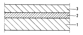
- the aim is to manufacture a semiconductor device, for example, a metal-base transistor in which ions are implanted in a monocrystalline silicon body 1 (see Figure) in order to obtain a buried silicide layer 2.
- a buried amorphous layer is first formed in the implantation, after which the buried silicide layer 2 is formed by a heat treatment.
- the amorphous layer is formed by implantation of a different element than that with which silicon of the silicon body is to form the buried silicide layer 2 subsequently.
- This other element may be, for example, a rare gas, for example argon, or it may be silicon.
- An amorphous silicon layer may be formed, for example, by means of a random implantation with a dose of 2,9 x 10¹⁴ silicon atoms per cm2 at an energy of 500 keV at a temperature of 80 K, whereby the amorphous silicon layer is given a thickness of 540 nm underneath a 200 nm thick top layer of monocrystalline silicon 3.
- a cobalt disilicide (CoSi2) layer having a thickness of 10 nm
- a cobalt implantation is necessary of approximately 2,6 x 10¹⁶ cobalt atoms per cm2. This may be done in a usual manner. It should be noted that amorphous silicon provides a high solubility for cobalt atoms.
- the amorphous silicon layer of 540 nm is converted into a cobalt silicide layer of 10 nm.
- the heat treatment takes, for example, four hours at 575° C and 0,5 hour at 1.000° C.
- the layer 3 acts as the emitter and the silicon body 1 as the collector.
- the present invention is obviously not limited to the example given, but may be varied in many ways by those skilled in the art.
- the amorphous layer may also be formed by implantation of, for example, cobalt atoms.
- a cobalt disilicide layer for example, a buried nickle disilicide layer may be formed. It is also possible to manufacture a permeable-base transistor by means of the method according to the invention.
Landscapes
- Bipolar Transistors (AREA)
- Electrodes Of Semiconductors (AREA)
Abstract
Description
- The invention relates to a method of manufacturing a semiconductor device whereby ions are implanted in a monocrystalline silicon body in order to obtain a buried silicide layer.
- The method indicated in the opening paragraph is known from European Patent Application no. 271.232.
The buried layes obtained by means of the known method have the disadvantage that they are too thick for many applications. They are unsuitable for, for example, so-called metal-base transistors in which the silicide layer serving as the base must be thinner than 10 nm. - The invention has for its object inter alia to avoid the said disadvantage at least to a considerable degree and is based on the insight that it is effective first to form an amorphous buried layer in the implantation.
According to the invention, therefore, the method mentioned in the opening paragraph is characterized in that first a buried amorphous layer is formed during the implantation and that subsequently the buried silicide layer is formed from the amorphous layer by a heat treatment.
Ions are often better soluble in amorphous silicon than in monocrystalline silicon, and the subsequent heat treatment then forms a silicide layer whose thickness is smaller than that of the amorphous layer originally formed.
The amorphous layer may be formed by implantation of a different element than that with which silicon of the silicon body is to form the buried silicide layer subsequently. The element with which silicon forms the silicide is then to be implanted separately.
For example, the amorphous layer is formed by implantation of silicon or a rare gas.
Preferably, the amorphous layer is formed by implantation of the element with which silicon of the silicon body is to form the buried silicide layer subsequently, for example, cobalt. - The invention will now be explained with reference to an embodiment and the accompanying Figure, which diagrammatically and in cross-section represents a portion of a semiconductor device in a stage of manufacture by means of the method according to the invention.
- In the present method, the aim is to manufacture a semiconductor device, for example, a metal-base transistor in which ions are implanted in a monocrystalline silicon body 1 (see Figure) in order to obtain a buried
silicide layer 2.
According to the invention, a buried amorphous layer is first formed in the implantation, after which the buriedsilicide layer 2 is formed by a heat treatment.
For example, the amorphous layer is formed by implantation of a different element than that with which silicon of the silicon body is to form the buriedsilicide layer 2 subsequently. This other element may be, for example, a rare gas, for example argon, or it may be silicon.
An amorphous silicon layer may be formed, for example, by means of a random implantation with a dose of 2,9 x 10¹⁴ silicon atoms per cm² at an energy of 500 keV at a temperature of 80 K, whereby the amorphous silicon layer is given a thickness of 540 nm underneath a 200 nm thick top layer ofmonocrystalline silicon 3.
To obtain a cobalt disilicide (CoSi₂) layer having a thickness of 10 nm, a cobalt implantation is necessary of approximately 2,6 x 10¹⁶ cobalt atoms per cm². This may be done in a usual manner.
It should be noted that amorphous silicon provides a high solubility for cobalt atoms.
During the ensuing heat treatment, the amorphous silicon layer of 540 nm is converted into a cobalt silicide layer of 10 nm. The heat treatment takes, for example, four hours at 575° C and 0,5 hour at 1.000° C.
In the metal-base transistor, which may be manufactured in usual manner in all other respects, thelayer 3 acts as the emitter and thesilicon body 1 as the collector.
The present invention is obviously not limited to the example given, but may be varied in many ways by those skilled in the art. Thus the amorphous layer may also be formed by implantation of, for example, cobalt atoms. Instead of a cobalt disilicide layer, for example, a buried nickle disilicide layer may be formed. It is also possible to manufacture a permeable-base transistor by means of the method according to the invention.
Claims (6)
- A method of manufacturing a semiconductor device whereby ions are implanted in a monocrystalline silicon body in order to obtain a buried silicide layer, characterized in that first a buried amorphous layer is formed during the implantation and that subsequently the buried silicide layer is formed from the amorphous layer by a heat treatment.
- A method as claimed in Claim 1, characterized in that the amorphous layer is formed by implantation of a different element than that with which silicon of the silicon body is to form the buried silicide layer subsequently.
- A method as claimed in Claim 2, characterized in that the amorphous layer is formed by implantation of silicon.
- A method as claimed in Claim 2, characterized in that the amorphous layer is formed by implantation of a rare gas.
- A method as claimed in Claim 1, characterized in that the amorphous layer is formed by implantation of the element with which silicon of the silicon body is to form the buried silicide layer subsequently.
- A method as claimed in Claim 5, characterized in that the amorphous layer is formed by implantation of cobalt.
Applications Claiming Priority (2)
| Application Number | Priority Date | Filing Date | Title |
|---|---|---|---|
| EP91200635 | 1991-03-21 | ||
| EP91200635 | 1991-03-21 |
Publications (3)
| Publication Number | Publication Date |
|---|---|
| EP0504987A2 true EP0504987A2 (en) | 1992-09-23 |
| EP0504987A3 EP0504987A3 (en) | 1992-10-21 |
| EP0504987B1 EP0504987B1 (en) | 1995-10-04 |
Family
ID=8207561
Family Applications (1)
| Application Number | Title | Priority Date | Filing Date |
|---|---|---|---|
| EP92200708A Expired - Lifetime EP0504987B1 (en) | 1991-03-21 | 1992-03-12 | Method of manufacturing a semiconductor device having a semiconductor body with a buried silicide layer |
Country Status (4)
| Country | Link |
|---|---|
| US (1) | US5236872A (en) |
| EP (1) | EP0504987B1 (en) |
| JP (1) | JPH07109833B2 (en) |
| DE (1) | DE69205193T2 (en) |
Cited By (1)
| Publication number | Priority date | Publication date | Assignee | Title |
|---|---|---|---|---|
| US6803273B1 (en) * | 1997-12-23 | 2004-10-12 | Texas Instruments Incorporated | Method to salicide source-line in flash memory with STI |
Families Citing this family (11)
| Publication number | Priority date | Publication date | Assignee | Title |
|---|---|---|---|---|
| US5290715A (en) * | 1991-12-31 | 1994-03-01 | U.S. Philips Corporation | Method of making dielectrically isolated metal base transistors and permeable base transistors |
| US5963838A (en) * | 1993-06-22 | 1999-10-05 | Kabushiki Kaisha Toshiba | Method of manufacturing a semiconductor device having wiring layers within the substrate |
| US5661044A (en) * | 1993-11-24 | 1997-08-26 | Lockheed Martin Energy Systems, Inc. | Processing method for forming dislocation-free SOI and other materials for semiconductor use |
| JP2978736B2 (en) * | 1994-06-21 | 1999-11-15 | 日本電気株式会社 | Method for manufacturing semiconductor device |
| GB9525784D0 (en) * | 1995-12-16 | 1996-02-14 | Philips Electronics Nv | Hot carrier transistors and their manufacture |
| US6841441B2 (en) | 2003-01-08 | 2005-01-11 | Chartered Semiconductor Manufacturing Ltd. | Method to produce dual gates (one metal and one poly or metal silicide) for CMOS devices using sputtered metal deposition, metallic ion implantation, or silicon implantation, and laser annealing |
| FR2864336B1 (en) * | 2003-12-23 | 2006-04-28 | Commissariat Energie Atomique | METHOD FOR SEALING TWO PLATES WITH FORMATION OF AN OHMIC CONTACT BETWEEN THEM |
| US8089137B2 (en) | 2009-01-07 | 2012-01-03 | Macronix International Co., Ltd. | Integrated circuit memory with single crystal silicon on silicide driver and manufacturing method |
| US8093661B2 (en) * | 2009-01-07 | 2012-01-10 | Macronix International Co., Ltd. | Integrated circuit device with single crystal silicon on silicide and manufacturing method |
| TWI398974B (en) * | 2009-01-07 | 2013-06-11 | Macronix Int Co Ltd | Integrated circuit device with single crystal silicon on silicide and manufacturing method |
| KR101801077B1 (en) * | 2012-01-10 | 2017-11-27 | 삼성전자주식회사 | Method of forming semiconductor device having buried wiring and related device |
Family Cites Families (10)
| Publication number | Priority date | Publication date | Assignee | Title |
|---|---|---|---|---|
| BE792589A (en) * | 1971-10-06 | 1973-03-30 | Ibm | PROCESS FOR OBTAINING SEMICONDUCTOR STRUCTURES BY IMPLANTATION OF IONS |
| US4096622A (en) * | 1975-07-31 | 1978-06-27 | General Motors Corporation | Ion implanted Schottky barrier diode |
| US4558507A (en) * | 1982-11-12 | 1985-12-17 | Nec Corporation | Method of manufacturing semiconductor device |
| JPS59210642A (en) * | 1983-05-16 | 1984-11-29 | Hitachi Ltd | Manufacture of semiconductor device |
| JPS60117738A (en) * | 1983-11-30 | 1985-06-25 | Sanken Electric Co Ltd | Manufacture of semiconductor device |
| US4875082A (en) * | 1986-06-20 | 1989-10-17 | Ford Aerospace Corporation | Schottky barrier photodiode structure |
| SE454309B (en) * | 1986-08-29 | 1988-04-18 | Stiftelsen Inst Mikrovags | PROCEDURE TO MAKE THIN LEADING OR SEMI-CONDUCTIVE LAYERS EMBEDDED IN SILICONE MEDIUM ATLANT IMPLANTATION |
| US4816421A (en) * | 1986-11-24 | 1989-03-28 | American Telephone And Telegraph Company, At&T Bell Laboratories | Method of making a heteroepitaxial structure by mesotaxy induced by buried implantation |
| JPH02220444A (en) * | 1989-02-21 | 1990-09-03 | Seiko Epson Corp | Semiconductor device manufacturing method |
| US5122479A (en) * | 1991-04-11 | 1992-06-16 | At&T Bell Laboratories | Semiconductor device comprising a silicide layer, and method of making the device |
-
1992
- 1992-03-09 US US07/848,612 patent/US5236872A/en not_active Expired - Fee Related
- 1992-03-12 EP EP92200708A patent/EP0504987B1/en not_active Expired - Lifetime
- 1992-03-12 DE DE69205193T patent/DE69205193T2/en not_active Expired - Fee Related
- 1992-03-18 JP JP4062415A patent/JPH07109833B2/en not_active Expired - Fee Related
Cited By (1)
| Publication number | Priority date | Publication date | Assignee | Title |
|---|---|---|---|---|
| US6803273B1 (en) * | 1997-12-23 | 2004-10-12 | Texas Instruments Incorporated | Method to salicide source-line in flash memory with STI |
Also Published As
| Publication number | Publication date |
|---|---|
| DE69205193D1 (en) | 1995-11-09 |
| DE69205193T2 (en) | 1996-05-02 |
| EP0504987B1 (en) | 1995-10-04 |
| US5236872A (en) | 1993-08-17 |
| EP0504987A3 (en) | 1992-10-21 |
| JPH07109833B2 (en) | 1995-11-22 |
| JPH0590279A (en) | 1993-04-09 |
Similar Documents
| Publication | Publication Date | Title |
|---|---|---|
| JP2585489B2 (en) | Method for manufacturing semiconductor device made of silicon | |
| EP0504987A2 (en) | Method of manufacturing a semiconductor device having a semiconductor body with a buried silicide layer | |
| US4977098A (en) | Method of forming a self-aligned bipolar transistor using amorphous silicon | |
| JPH0777259B2 (en) | Method for manufacturing polycrystalline silicon resistor having desired temperature coefficient | |
| JPH0727965B2 (en) | Method for manufacturing device including embedded SiO 2 layer | |
| US7968954B2 (en) | Intermediate semiconductor device having nitrogen concentration profile | |
| US4764478A (en) | Method of manufacturing MOS transistor by dual species implantation and rapid annealing | |
| JPH05102072A (en) | Semiconductor device including silicide layer and method of manufacturing the device | |
| JP2998330B2 (en) | SIMOX substrate and method of manufacturing the same | |
| MY125505A (en) | Optimized reachthrough implant for simultaneously forming an mos capacitor. | |
| US4837174A (en) | Method for producing thin conductive and semi-conductive layers in mono-crystal silicon | |
| EP0573241A2 (en) | Semiconductor devices with a double layered silicide structure and process of making it | |
| US4472210A (en) | Method of making a semiconductor device to improve conductivity of amorphous silicon films | |
| JP3165051B2 (en) | Semiconductor element well formation method | |
| EP0736224B1 (en) | Method of forming a thermally stable silicide | |
| JPH069227B2 (en) | Method for manufacturing semiconductor substrate | |
| JPS6269555A (en) | Manufacturing transistor | |
| JPH026222B2 (en) | ||
| Shibata et al. | Resistivity changes in laser‐annealed polycrystalline silicon during thermal annealing | |
| JP3287839B2 (en) | Method of forming polycide film | |
| JPH0521461A (en) | Method for manufacturing semiconductor device | |
| KR100325297B1 (en) | Method for manufacturing semiconductor device | |
| JPH05206045A (en) | Method for manufacturing semiconductor device | |
| JPH08274111A (en) | Bipolar silicon transistor and manufacturing method thereof | |
| JPH03265131A (en) | Manufacture of semiconductor device |
Legal Events
| Date | Code | Title | Description |
|---|---|---|---|
| PUAI | Public reference made under article 153(3) epc to a published international application that has entered the european phase |
Free format text: ORIGINAL CODE: 0009012 |
|
| PUAL | Search report despatched |
Free format text: ORIGINAL CODE: 0009013 |
|
| AK | Designated contracting states |
Kind code of ref document: A2 Designated state(s): DE FR GB IT NL |
|
| AK | Designated contracting states |
Kind code of ref document: A3 Designated state(s): DE FR GB IT NL |
|
| 17P | Request for examination filed |
Effective date: 19930405 |
|
| 17Q | First examination report despatched |
Effective date: 19930803 |
|
| GRAA | (expected) grant |
Free format text: ORIGINAL CODE: 0009210 |
|
| AK | Designated contracting states |
Kind code of ref document: B1 Designated state(s): DE FR GB IT NL |
|
| PG25 | Lapsed in a contracting state [announced via postgrant information from national office to epo] |
Ref country code: NL Free format text: LAPSE BECAUSE OF FAILURE TO SUBMIT A TRANSLATION OF THE DESCRIPTION OR TO PAY THE FEE WITHIN THE PRESCRIBED TIME-LIMIT Effective date: 19951004 |
|
| REF | Corresponds to: |
Ref document number: 69205193 Country of ref document: DE Date of ref document: 19951109 |
|
| ITF | It: translation for a ep patent filed | ||
| ET | Fr: translation filed | ||
| NLV1 | Nl: lapsed or annulled due to failure to fulfill the requirements of art. 29p and 29m of the patents act | ||
| PLBE | No opposition filed within time limit |
Free format text: ORIGINAL CODE: 0009261 |
|
| STAA | Information on the status of an ep patent application or granted ep patent |
Free format text: STATUS: NO OPPOSITION FILED WITHIN TIME LIMIT |
|
| 26N | No opposition filed | ||
| REG | Reference to a national code |
Ref country code: FR Ref legal event code: CD |
|
| REG | Reference to a national code |
Ref country code: GB Ref legal event code: IF02 |
|
| REG | Reference to a national code |
Ref country code: GB Ref legal event code: 746 Effective date: 20021017 |
|
| REG | Reference to a national code |
Ref country code: FR Ref legal event code: D6 |
|
| PGFP | Annual fee paid to national office [announced via postgrant information from national office to epo] |
Ref country code: FR Payment date: 20030328 Year of fee payment: 12 |
|
| PGFP | Annual fee paid to national office [announced via postgrant information from national office to epo] |
Ref country code: GB Payment date: 20030331 Year of fee payment: 12 |
|
| PGFP | Annual fee paid to national office [announced via postgrant information from national office to epo] |
Ref country code: DE Payment date: 20030515 Year of fee payment: 12 |
|
| PG25 | Lapsed in a contracting state [announced via postgrant information from national office to epo] |
Ref country code: GB Free format text: LAPSE BECAUSE OF NON-PAYMENT OF DUE FEES Effective date: 20040312 |
|
| PG25 | Lapsed in a contracting state [announced via postgrant information from national office to epo] |
Ref country code: DE Free format text: LAPSE BECAUSE OF NON-PAYMENT OF DUE FEES Effective date: 20041001 |
|
| GBPC | Gb: european patent ceased through non-payment of renewal fee |
Effective date: 20040312 |
|
| PG25 | Lapsed in a contracting state [announced via postgrant information from national office to epo] |
Ref country code: FR Free format text: LAPSE BECAUSE OF NON-PAYMENT OF DUE FEES Effective date: 20041130 |
|
| REG | Reference to a national code |
Ref country code: FR Ref legal event code: ST |
|
| PG25 | Lapsed in a contracting state [announced via postgrant information from national office to epo] |
Ref country code: IT Free format text: LAPSE BECAUSE OF NON-PAYMENT OF DUE FEES;WARNING: LAPSES OF ITALIAN PATENTS WITH EFFECTIVE DATE BEFORE 2007 MAY HAVE OCCURRED AT ANY TIME BEFORE 2007. THE CORRECT EFFECTIVE DATE MAY BE DIFFERENT FROM THE ONE RECORDED. Effective date: 20050312 |