EP0501824A2 - Optischer Strahlablenker mit Adressierung durch unterteilte Öffnungen - Google Patents
Optischer Strahlablenker mit Adressierung durch unterteilte Öffnungen Download PDFInfo
- Publication number
- EP0501824A2 EP0501824A2 EP92301729A EP92301729A EP0501824A2 EP 0501824 A2 EP0501824 A2 EP 0501824A2 EP 92301729 A EP92301729 A EP 92301729A EP 92301729 A EP92301729 A EP 92301729A EP 0501824 A2 EP0501824 A2 EP 0501824A2
- Authority
- EP
- European Patent Office
- Prior art keywords
- stripe electrodes
- interconnects
- electrodes
- optical beam
- stripe
- Prior art date
- Legal status (The legal status is an assumption and is not a legal conclusion. Google has not performed a legal analysis and makes no representation as to the accuracy of the status listed.)
- Granted
Links
Images


Classifications
-
- G—PHYSICS
- G02—OPTICS
- G02F—OPTICAL DEVICES OR ARRANGEMENTS FOR THE CONTROL OF LIGHT BY MODIFICATION OF THE OPTICAL PROPERTIES OF THE MEDIA OF THE ELEMENTS INVOLVED THEREIN; NON-LINEAR OPTICS; FREQUENCY-CHANGING OF LIGHT; OPTICAL LOGIC ELEMENTS; OPTICAL ANALOGUE/DIGITAL CONVERTERS
- G02F1/00—Devices or arrangements for the control of the intensity, colour, phase, polarisation or direction of light arriving from an independent light source, e.g. switching, gating or modulating; Non-linear optics
- G02F1/29—Devices or arrangements for the control of the intensity, colour, phase, polarisation or direction of light arriving from an independent light source, e.g. switching, gating or modulating; Non-linear optics for the control of the position or the direction of light beams, i.e. deflection
- G02F1/292—Devices or arrangements for the control of the intensity, colour, phase, polarisation or direction of light arriving from an independent light source, e.g. switching, gating or modulating; Non-linear optics for the control of the position or the direction of light beams, i.e. deflection by controlled diffraction or phased-array beam steering
-
- G—PHYSICS
- G02—OPTICS
- G02F—OPTICAL DEVICES OR ARRANGEMENTS FOR THE CONTROL OF LIGHT BY MODIFICATION OF THE OPTICAL PROPERTIES OF THE MEDIA OF THE ELEMENTS INVOLVED THEREIN; NON-LINEAR OPTICS; FREQUENCY-CHANGING OF LIGHT; OPTICAL LOGIC ELEMENTS; OPTICAL ANALOGUE/DIGITAL CONVERTERS
- G02F1/00—Devices or arrangements for the control of the intensity, colour, phase, polarisation or direction of light arriving from an independent light source, e.g. switching, gating or modulating; Non-linear optics
- G02F1/01—Devices or arrangements for the control of the intensity, colour, phase, polarisation or direction of light arriving from an independent light source, e.g. switching, gating or modulating; Non-linear optics for the control of the intensity, phase, polarisation or colour
- G02F1/13—Devices or arrangements for the control of the intensity, colour, phase, polarisation or direction of light arriving from an independent light source, e.g. switching, gating or modulating; Non-linear optics for the control of the intensity, phase, polarisation or colour based on liquid crystals, e.g. single liquid crystal display cells
- G02F1/133—Constructional arrangements; Operation of liquid crystal cells; Circuit arrangements
- G02F1/1333—Constructional arrangements; Manufacturing methods
- G02F1/1343—Electrodes
- G02F1/134309—Electrodes characterised by their geometrical arrangement
-
- H—ELECTRICITY
- H01—ELECTRIC ELEMENTS
- H01Q—ANTENNAS, i.e. RADIO AERIALS
- H01Q3/00—Arrangements for changing or varying the orientation or the shape of the directional pattern of the waves radiated from an antenna or antenna system
- H01Q3/26—Arrangements for changing or varying the orientation or the shape of the directional pattern of the waves radiated from an antenna or antenna system varying the relative phase or relative amplitude of energisation between two or more active radiating elements; varying the distribution of energy across a radiating aperture
- H01Q3/2676—Optically controlled phased array
-
- G—PHYSICS
- G02—OPTICS
- G02F—OPTICAL DEVICES OR ARRANGEMENTS FOR THE CONTROL OF LIGHT BY MODIFICATION OF THE OPTICAL PROPERTIES OF THE MEDIA OF THE ELEMENTS INVOLVED THEREIN; NON-LINEAR OPTICS; FREQUENCY-CHANGING OF LIGHT; OPTICAL LOGIC ELEMENTS; OPTICAL ANALOGUE/DIGITAL CONVERTERS
- G02F2203/00—Function characteristic
- G02F2203/24—Function characteristic beam steering
Definitions
- phase shifting elements of the present invention illustratively comprise liquid crystal devices and may generally be of the type suggested in the above-mentioned Huignard et al. patent, but which are more specifically similar to the phase shifting elements disclosed and described in the Dorschner et al. (701′) patent.
- FIG. 1 there is shown, in diagrammatical cross-sectional view, a liquid crystal beam steering device 10 of the type described for use in the present invention, and which is a simplified representation of the beam steerer described in the Dorschner et al. (701′) patent.
- Device 10 comprises a liquid crystal cell having windows 12 and 14 which are optically transparent at the frequency range of interest.
- Common electrode 16, affixed to window 12 is electrically conductive and optically transparent.
- Electrodes 181, 182, 183, . . ., referred to collectively as electrodes 18, affixed to window 14, comprise a plurality of electrically-conductive, optically-transparent stripes.
- electrodes 18 may be 4-10 micrometers ( ⁇ m) in width, and spaced from one another by approximately one ⁇ m.
- the space between windows 12 and 14 is filled with a layer of liquid crystal molecules 20, illustratively long, thin, rod-like organic molecules of the so-called "nematic" phase.
- the referenced Dorschner et al. patent teaches the use of alignment layers on the inner surfaces of windows 12 and 14 to properly align the liquid crystal molecules at the boundaries of layer 20.
- the appropriate alignment of the liquid crystal molecules such that liquid crystal cell 10 functions properly as a variable phase retarder, is parallel to the polarization of the incident light. It has also been determined that a preferable alignment of the liquid crystal molecules is orthogonal to the longitudinal edges of the stripe electrodes 18.
- the optical beam phase shifter 10 of FIG. 1 is responsive to a light source and beam forming network (not shown) which provide a polarized light beam 22, ranging from visible through far infrared.
- beam 22 is in the infrared spectrum, having a typical wavelength in the range of 9 to 11.5 ⁇ m, illustratively at 10.6 ⁇ m.
- Light beam 22, represented in part by rays 22a-22c, is directed onto window 14 of optical device 10.
- Light beam 22 may be incident perpendicular to the plane formed by stripe electrodes 18, or it may be incident obliquely, preferably such that its projection onto the plane formed by stripe electrodes 18 is parallel to the longitudinal direction of electrodes 18. In other words, the longitudinal edges of stripe electrodes 18 are parallel to the planes of incidence of rays 22a-22c.
- the potentials applied to the electrodes 18 onto which rays 22a, 22b and 22c are incident shown diagrammatically as staircase waveform 26a, are such as to cause the greatest retardation to emergent ray 24c, and the least retardation to emergent ray 24a.
- the wavefront 17 of the beam 24 which emerges from the optical beam deflector 10 is tilted with respect to the incident wavefront. If identical potential is applied to all electrodes 18, the refractive index of the liquid crystal layer 20 is uniform, and beam 24 is undeflected. It is therefore seen that the optical beam deflector 10 of FIG. 1 provides selective beam steering in accordance with the electrical potentials applied to stripe electrodes 18.
- control voltage signals to the individual stripe electrodes 18 for the purpose of beam steering is analogous to the methods used in conventional microwave radar beam steering as taught, for example, in Radar Handbook , M.I Skolnik, ed., McGraw-Hill, New York, 1970, at chapter 11.
- a plurality of control voltage signals being periodic in space and having a continuous progression of voltage steps within each period between a minimum value and a maximum value, may be applied to the multiplicity of stripe electrodes 18.
- cell windows 12 and 14 must exhibit low absorption of the infrared light having the wavelength emitted by a CO2 laser, typically at 10.6 ⁇ m.
- Typical candidates for the choice of cell windows 12 and 14 include semiconductors such as germanium, zinc selenide and gallium arsenide, or the halide salts, such as potassium chloride, all of which are relatively transparent to CO2 laser light.
- electrode 16, which provides electrical conductivity across cell window 12, and electrodes 18, which provide a multiplicity of individual zones of electrical conductivity on cell window 14, must also be substantially optically transparent at the above-mentioned wavelength.
- optically transparent electrodes 16 and 18 are preferably provided on cell windows 12 and 14 by a process of ion implantation, as disclosed in U.S. Patent No. 4,882,235, "Liquid Crystal Cell Windows,” issued November 21, 1989, to D.P. Resler, and assigned to the same assignee as the present invention, which patent is incorporated herein by reference.
- the illustrative beam steering device 10 of FIG. 1 operates in the transmission mode for light beam 22 incident on window 14 having stripe electrodes 18, the cited references suggest that many variations of this arrangement may be effected.
- light beam 22 may be incident on window 12 having common electrode 16 and emerge deflected from window 14.
- common electrode 16 may be reflective at the frequency range of interest, and light beam 22 would be incident on, and emerge deflected from window 14.
- stripe electrodes 18 may be optically reflective, and light beam 22 would be incident on, and emerge deflected from, window 12.
- a staircase of voltage 26a is applied to electrodes 18, the voltage levels chosen to result in a uniform staircase, or an approximation to a ramp, of phase shift across the aperture. Because the response of the liquid crystal is not linear, the voltage ramp does not necessarily comprise equal steps.
- the phase shifters may be operated modulo 2 ⁇ , as with microwave arrays, to avoid the requirement of large phase shifts.
- the resultant "sawtooth" distribution of phase is equivalent to a single continuous phase ramp, which acts like a prism and steers the input beam according to the degree of phase ramp imposed.
- the referenced Dorschner et al. (′701) patent discloses relatively large contact pads which underlie the stripe electrodes, and whose widths span a number of the stripes.
- Each contact pad is electrically coupled to a single electrode by a conductor which may typically be deposited into a via hole.
- the conductors are preferably spaced apart in a staggered configuration.
- the present invention discloses structure for combining the multiplicity of electrodes into a plurality of subarrays, wherein each subarray comprises a number of electrodes sufficient to provide an adequate distribution of beam steering angles for the intended application.
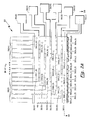
- FIGS. 2a and 2b there are shown diagrammatical plan and cross-sectional views, respectively, of a portion of a simplified beam steering assembly according to the principles of the present invention.
- the assembly includes a liquid crystal cell 52 having windows 40 and 44 and a layer of liquid crystal molecules 50 therebetween.
- cell 52 includes a common electrode 42 on an inner surface of window 44, and a multiplicity of stripe electrodes 30(1,1), 30(1,2), . . ., 30(1,6), 30(2,1), . . ., 30(2,6), . . ., 30(n,1), . . ., 30(n,6), referred to collectively as stripe electrodes 30, on an inner surface of window 40.
- the beam steering assembly of FIGS. 2a and 2b comprises a large array of striped phase shifters, wherein each phase shifter is formed by one of the stripe electrodes 30, the common electrode 42 and the liquid crystal molecules 50 therebetween.
- the phase shifters uniformly cover substantially the entire aperture of the beam steering assembly.
- a plurality of n subarrays 38(1), . . ., 38(n), referred to collectively as subarrays 38 are formed by jumper straps 32(1), 32(2), . . ., 32(6), referred to collectively as jumper straps 32.
- jumper strap 32(1) interconnects stripe electrodes 30(1,1), 30(2,1), . . ., and 30(n,1)
- jumper strap 32(2) interconnects stripe electrodes 30(1,2), 30(2,2), . . ., and 30(n,2); etc.
- Jumper strap 32(1) is connected to stripe electrode 30(1,1) by a conductor within via hole 34(1,1), to stripe electrode 30(2,1) by a conductor within via hole 34(2,1), . . ., and to stripe electrode 30(n,1) by a conductor within via hole 34(n,1).
- jumper straps 32(i) are connected to stripe electrodes 30(j,i) by the conductors within via holes 34(j,i), wherein j runs from 1 to the number of subarrays, n, and i runs from 1 to the number of phase shifters, M, within each subarray.
- Each jumper strap 32(i) terminates at a contact pad 36(i) for interconnection with external wiring for the purpose of application of control voltages thereto.
- common electrode 42 is coupled to a contact pad 48 for interconnection with an external lead for the purpose of application of a reference voltage thereto.
- every sixth electrode 30 is connected in parallel, and there are just six address lines which must be connected via contact pads 36 to external power supplies, instead of the thousands which would ordinarily be required for apertures of one cm or larger. These is also a single ground connection required at contact pad 48, independent of the number of electrodes 30 in a subarray 38, or in the entire array.
- each phase shifter is permanently connected in parallel to the corresponding phase shifter of each of the other subarrays 38. Thus, whatever spatial phase distribution is applied to one subarray 38 is repeated across the full aperture.
- M is the number of phase shifters in a subarray
- the number of addressing electrodes is M + 1.
- M is likely to be a rather large number, probably several hundred, possibly several thousand.
- M is small in comparison with the total number of phase shifters S in the entire array, there is a significant reduction of the number of required addressing lines. That is the case for practical applications.
- the leadout connections are fabricated as follows: a multiplicity of stripe electrodes 30 (one for each phase shifter) are formed on an optically transparent substrate 40 by ion implantation. Other means may be used, such as deposition of semi-transparent conducting thin films, but ion implantation has been found to be preferable from several key performance considerations, such as losses, optical index match, and laser damage levels.
- a thin-film insulating layer 46 such as silicon nitride or silicon dioxide, is then deposited over a small area including the terminating ends of electrodes 30. Via holes 34 are then formed in the thin-film insulating layer 46 using a photo-pattern and either plasma or chemical etching.
- the via holes 34 are arranged in a pattern appropriate for the desired electrode grouping; i.e., at every Mth electrode in a cyclic manner for an M-phase-shifter subarray architecture, as shown in FIGS. 2a and 2b.
- Thin-film metal interconnect lines 32 are then deposited through another photo-pattern on top of insulating layer 46, thereby electrically connecting the appropriate electrodes 30 through via holes 34.
- As many metal interconnect lines 32 are used as there are independently addressable connections for the subarray architecture chosen.
- the metal interconnect lines 32 terminate at the substrate periphery into bonding pads 36 which may illustratively be subsequently wire-bonded to pins on a flatpack device holder (not shown).
- the beam steering device illustrated in the present embodiment comprises a liquid crystal cell 52 having planar windows 40 and 44, it will be recognized by those of skill in the art that electrodes 40 and 42 may be affixed to non-planar surfaces, e.g., convex or concave surfaces, which have the quality of being of good optical figure.
- the subarray-addressed optical beam steerer of the present invention may be operated similarly to a conventional phased array, that is, a step-wise approximation to a phase ramp across the beam steering aperture is formed by the application of a corresponding staircase profile of voltages to the electrodes (see FIG. 1).
- the phase ramps may be applied modulo 2 ⁇ with maximum amplitude 2 ⁇ .
- only a limited number of ramp periods can be synthesized because only a limited number of phase Shifters, namely M, the number in each subarray, are independently addressable. This limits the number of addressable beam positions; however, a rather large number of positions are nevertheless possible, even for moderate subarray sizes, as is discussed below.
- Ramps with periods N ⁇ O which are integral factors of the subarray period M ⁇ O can be applied without any discontinuities at the subarray edges. That is an important consideration for maintaining low levels of sidelobes.
- subarrays with larger numbers of phase shifters include smaller steering angles.
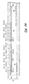
- subarrays of 48 phase shifters give the distribution of steering angles shown in FIG. 3, for the case of exact factorial periods (labeled "ramp pitch" here).
- a spacing ⁇ O of one wavelength between the stripe electrodes of the phase shifters has been assumed. Only those angles subtending a ⁇ 10° field of regard are shown; that is a fairly typical range of interest. It may be seen from FIG. 3 that the distribution of obtainable angles is fairly uniform. This trend toward uniform angle spacing increases rapidly as the number of elements in the subarray increases.
- a beam steerer having subarrays of 256 phase shifters has been built and tested and found to provide a large number of beam positions, fairly uniformly distributed within the above-mentioned ⁇ 10° field of regard.
- additional periods can be formed by the linear superposition of the above exact periods.
- Other effective periods can also be formed by the combination of periods which sum to the subarray dimension.
Landscapes
- Physics & Mathematics (AREA)
- Nonlinear Science (AREA)
- General Physics & Mathematics (AREA)
- Optics & Photonics (AREA)
- Geometry (AREA)
- Mathematical Physics (AREA)
- Chemical & Material Sciences (AREA)
- Crystallography & Structural Chemistry (AREA)
- Liquid Crystal (AREA)
- Optical Radar Systems And Details Thereof (AREA)
- Optical Modulation, Optical Deflection, Nonlinear Optics, Optical Demodulation, Optical Logic Elements (AREA)
Applications Claiming Priority (2)
| Application Number | Priority Date | Filing Date | Title |
|---|---|---|---|
| US07/662,094 US5093740A (en) | 1991-02-28 | 1991-02-28 | Optical beam steerer having subaperture addressing |
| US662094 | 1991-02-28 |
Publications (3)
| Publication Number | Publication Date |
|---|---|
| EP0501824A2 true EP0501824A2 (de) | 1992-09-02 |
| EP0501824A3 EP0501824A3 (en) | 1993-05-05 |
| EP0501824B1 EP0501824B1 (de) | 1997-08-27 |
Family
ID=24656358
Family Applications (1)
| Application Number | Title | Priority Date | Filing Date |
|---|---|---|---|
| EP92301729A Expired - Lifetime EP0501824B1 (de) | 1991-02-28 | 1992-02-28 | Optischer Strahlablenker mit Adressierung durch unterteilte Öffnungen |
Country Status (4)
| Country | Link |
|---|---|
| US (1) | US5093740A (de) |
| EP (1) | EP0501824B1 (de) |
| JP (1) | JP3512429B2 (de) |
| DE (1) | DE69221751T2 (de) |
Cited By (2)
| Publication number | Priority date | Publication date | Assignee | Title |
|---|---|---|---|---|
| WO1999024866A1 (fr) * | 1997-11-05 | 1999-05-20 | Zhu, Runshu | Dispositif a reseau de phase optique et procede de realisation |
| EP0899606A3 (de) * | 1997-07-31 | 1999-12-22 | Sharp Kabushiki Kaisha | Räumlicher Lichtmodulator und Anzeigevorrichtung |
Families Citing this family (28)
| Publication number | Priority date | Publication date | Assignee | Title |
|---|---|---|---|---|
| JPH0684031B2 (ja) * | 1984-08-16 | 1994-10-26 | 三菱マテリアル株式会社 | 射出成形方法 |
| EP0608458B1 (de) * | 1993-01-29 | 2002-01-02 | Citizen Watch Co. Ltd. | Verfahren zur Steuerung einer optischen Modulationsvorrichtung |
| US5373151A (en) * | 1993-10-04 | 1994-12-13 | Raytheon Company | Optical system including focal plane array compensation technique for focusing and periodically defocusing a beam |
| US5400161A (en) * | 1993-10-04 | 1995-03-21 | Raytheon Company | Optical system including focus-defocus focal plane array compensation technique using liquid crystal phased array |
| US5943159A (en) * | 1996-05-14 | 1999-08-24 | Zhu; Tom Yuxin | Method and apparatus for optical beam steering |
| JPH1041857A (ja) * | 1996-07-23 | 1998-02-13 | Nec Corp | 移動通信システム用送信装置 |
| US6456419B1 (en) | 2000-09-29 | 2002-09-24 | Innovative Technology Licensing, Llc | Frequency modulated liquid crystal beamsteering device |
| US6490076B2 (en) | 2001-01-11 | 2002-12-03 | Hrl Laboratories, Llc | Optical phased array for depolarized optical beam control |
| US6643054B1 (en) | 2001-01-22 | 2003-11-04 | Carl-Zeiss-Stiftung | Beam deflector, switching system comprising beam deflectors as well as method for selectively coupling terminals for optical signals |
| US6618189B2 (en) | 2001-04-10 | 2003-09-09 | Hrl Laboratories, Llc | Radio frequency wave and optical beam steerer combination |
| US6809307B2 (en) * | 2001-09-28 | 2004-10-26 | Raytheon Company | System and method for effecting high-power beam control with adaptive optics in low power beam path |
| US6849841B2 (en) * | 2001-09-28 | 2005-02-01 | Raytheon Company | System and method for effecting high-power beam control with outgoing wavefront correction utilizing holographic sampling at primary mirror, phase conjugation, and adaptive optics in low power beam path |
| JP4382317B2 (ja) * | 2001-12-06 | 2009-12-09 | シチズンホールディングス株式会社 | 液晶可変波長フィルタ装置 |
| US7215472B2 (en) * | 2004-08-12 | 2007-05-08 | Raytheon Company | Wide-angle beam steering system |
| GB0608055D0 (en) * | 2006-04-24 | 2006-05-31 | Univ Cambridge Tech | Liquid crystal devices |
| US8059254B1 (en) * | 2008-06-04 | 2011-11-15 | Raytheon Company | Transparent heatsink/structure/interconnect for tiling space based optical components |
| US8362410B2 (en) | 2010-07-26 | 2013-01-29 | Raytheon Company | Source-independent beam director and control system for a high-energy electromagnetic radiation source |
| US20120068880A1 (en) | 2010-09-17 | 2012-03-22 | Raytheon Company | System and Method for Dual-Band Antenna Pointing, Acquisition, And Tracking |
| NZ702327A (en) | 2012-05-24 | 2016-03-31 | Raytheon Co | Liquid crystal control structure, tip-tilt-focus optical phased array and high power adaptive optic |
| KR101996655B1 (ko) * | 2012-12-26 | 2019-07-05 | 엘지디스플레이 주식회사 | 홀로그램 표시 장치 |
| EP3004979B1 (de) | 2013-05-24 | 2019-01-16 | Raytheon Company | Adaptiveoptik mit flüssigkristallanordnungsvorrichtung und mäanderwiderständen |
| US9575341B2 (en) * | 2014-06-28 | 2017-02-21 | Intel Corporation | Solid state LIDAR circuit with waveguides tunable to separate phase offsets |
| CN109581696A (zh) * | 2017-09-28 | 2019-04-05 | 北京万集科技股份有限公司 | 一种波导移相器及其制备方法 |
| DE102018206140A1 (de) * | 2018-04-20 | 2019-10-24 | Bayerische Motoren Werke Aktiengesellschaft | Abdeckelement, System und Vorrichtung |
| JP2019200258A (ja) * | 2018-05-15 | 2019-11-21 | 凸版印刷株式会社 | 光偏向装置 |
| US11143860B1 (en) | 2019-04-29 | 2021-10-12 | United States Of America As Represented By The Secretary Of The Air Force | Photonic crystal-based optical steering |
| CN112817009B (zh) * | 2020-12-30 | 2022-10-18 | 西安电子科技大学 | 基于二维光学相控阵的抗干扰探测成像系统和方法 |
| KR102721980B1 (ko) | 2022-02-24 | 2024-10-25 | 삼성전자주식회사 | 기판 정렬 장치 및 이를 이용한 기판 정렬 방법 |
Family Cites Families (11)
| Publication number | Priority date | Publication date | Assignee | Title |
|---|---|---|---|---|
| FR2134160B1 (de) * | 1971-04-22 | 1975-01-17 | Commissariat Energie Atomique | |
| US3915548A (en) * | 1973-04-30 | 1975-10-28 | Hughes Aircraft Co | Holographic lens and liquid crystal image source for head-up display |
| US4066334A (en) * | 1975-01-06 | 1978-01-03 | National Research Development Corporation | Liquid crystal light deflector |
| US4115747A (en) | 1976-12-27 | 1978-09-19 | Heihachi Sato | Optical modulator using a controllable diffraction grating |
| FR2541784B1 (fr) * | 1983-02-25 | 1986-05-16 | Thomson Csf | Dispositif de deflexion statique d'un faisceau infra-rouge |
| US4958914A (en) * | 1986-06-27 | 1990-09-25 | Hughes Aircraft Company | Optical intensity-to-position mapping and light deflector apparatus and method |
| US4937539A (en) * | 1987-08-19 | 1990-06-26 | Hughes Aircraft Company | Phased array for optical beam control |
| US4824215A (en) * | 1988-01-22 | 1989-04-25 | Xtalite Technology Limited/La Technologie Xtalite Limitee | Liquid crystal display apparatus |
| US4882235A (en) * | 1988-03-02 | 1989-11-21 | Raytheon Company | Liquid crystal cell window |
| US4964701A (en) * | 1988-10-04 | 1990-10-23 | Raytheon Company | Deflector for an optical beam |
| US5018835A (en) * | 1989-01-03 | 1991-05-28 | Raytheon Company | Deflector for an optical beam including refractive means |
-
1991
- 1991-02-28 US US07/662,094 patent/US5093740A/en not_active Expired - Lifetime
-
1992
- 1992-02-28 DE DE69221751T patent/DE69221751T2/de not_active Expired - Lifetime
- 1992-02-28 EP EP92301729A patent/EP0501824B1/de not_active Expired - Lifetime
- 1992-02-28 JP JP04341992A patent/JP3512429B2/ja not_active Expired - Fee Related
Cited By (3)
| Publication number | Priority date | Publication date | Assignee | Title |
|---|---|---|---|---|
| EP0899606A3 (de) * | 1997-07-31 | 1999-12-22 | Sharp Kabushiki Kaisha | Räumlicher Lichtmodulator und Anzeigevorrichtung |
| US6094249A (en) * | 1997-07-31 | 2000-07-25 | Sharp Kabushiki Kaisha | Spatial light modulator and display with reduced electrical connectivity requirement |
| WO1999024866A1 (fr) * | 1997-11-05 | 1999-05-20 | Zhu, Runshu | Dispositif a reseau de phase optique et procede de realisation |
Also Published As
| Publication number | Publication date |
|---|---|
| DE69221751T2 (de) | 1998-04-09 |
| EP0501824A3 (en) | 1993-05-05 |
| EP0501824B1 (de) | 1997-08-27 |
| DE69221751D1 (de) | 1997-10-02 |
| JP3512429B2 (ja) | 2004-03-29 |
| JPH0580358A (ja) | 1993-04-02 |
| US5093740A (en) | 1992-03-03 |
Similar Documents
| Publication | Publication Date | Title |
|---|---|---|
| EP0501824B1 (de) | Optischer Strahlablenker mit Adressierung durch unterteilte Öffnungen | |
| EP0501825B1 (de) | Verfahren zur Strahlsteuerung in einem durch fein unterteilte Öffnungen adressierten optischen Strahlablenker | |
| EP0363084B1 (de) | Ablenkungselement für einen optischen Strahl | |
| US5151814A (en) | Phased array for optical beam control | |
| US4937539A (en) | Phased array for optical beam control | |
| US5440654A (en) | Fiber optic switching system | |
| US6456419B1 (en) | Frequency modulated liquid crystal beamsteering device | |
| US5528414A (en) | Two dimensional electro-optic modulator array | |
| US4813766A (en) | Optical time delay apparatus | |
| US5061048A (en) | Apparatus for optical beam steering using non-linear optical polymers | |
| US4447815A (en) | Lens for electronic scanning in the polarization plane | |
| US4882235A (en) | Liquid crystal cell window | |
| US6832028B2 (en) | Liquid crystal adaptive coupler for steering a light beam relative to a light-receiving end of an optical waveguide | |
| US6128421A (en) | Electro-optical phased array beam modulator | |
| EP0352302B1 (de) | Phasengesteuerter lichtablenker | |
| US4693561A (en) | Amorphous silicon spatial light modulator | |
| JPS62502783A (ja) | 横方向に駆動される電子光学的ゲ−トを備える線形光弁アレイおよびその製造方法 | |
| US5262796A (en) | Optoelectronic scanning microwave antenna | |
| US8089677B2 (en) | Dynamic optical grating device and associated method for modulating light | |
| US20230418049A1 (en) | Two-layer optical beam steering device, system, method of utilization, and method of fabrication | |
| GB2225122A (en) | An apparatus for producing a phase shift in a beam of electromagnetic radiation | |
| Fubini | Stripline radiators | |
| Cassarly et al. | Phase control of coherent diode laser arrays using liquid crystals | |
| KR20250145117A (ko) | 광 도파관 | |
| CN118092028A (zh) | 波束扫描装置及电子设备 |
Legal Events
| Date | Code | Title | Description |
|---|---|---|---|
| PUAI | Public reference made under article 153(3) epc to a published international application that has entered the european phase |
Free format text: ORIGINAL CODE: 0009012 |
|
| AK | Designated contracting states |
Kind code of ref document: A2 Designated state(s): DE FR GB |
|
| PUAL | Search report despatched |
Free format text: ORIGINAL CODE: 0009013 |
|
| AK | Designated contracting states |
Kind code of ref document: A3 Designated state(s): DE FR GB |
|
| 17P | Request for examination filed |
Effective date: 19930922 |
|
| 17Q | First examination report despatched |
Effective date: 19950721 |
|
| GRAG | Despatch of communication of intention to grant |
Free format text: ORIGINAL CODE: EPIDOS AGRA |
|
| GRAH | Despatch of communication of intention to grant a patent |
Free format text: ORIGINAL CODE: EPIDOS IGRA |
|
| GRAH | Despatch of communication of intention to grant a patent |
Free format text: ORIGINAL CODE: EPIDOS IGRA |
|
| GRAA | (expected) grant |
Free format text: ORIGINAL CODE: 0009210 |
|
| AK | Designated contracting states |
Kind code of ref document: B1 Designated state(s): DE FR GB |
|
| REF | Corresponds to: |
Ref document number: 69221751 Country of ref document: DE Date of ref document: 19971002 |
|
| ET | Fr: translation filed | ||
| PLBE | No opposition filed within time limit |
Free format text: ORIGINAL CODE: 0009261 |
|
| 26N | No opposition filed | ||
| REG | Reference to a national code |
Ref country code: GB Ref legal event code: IF02 |
|
| PGFP | Annual fee paid to national office [announced via postgrant information from national office to epo] |
Ref country code: FR Payment date: 20110218 Year of fee payment: 20 Ref country code: DE Payment date: 20110223 Year of fee payment: 20 |
|
| PGFP | Annual fee paid to national office [announced via postgrant information from national office to epo] |
Ref country code: GB Payment date: 20110223 Year of fee payment: 20 |
|
| REG | Reference to a national code |
Ref country code: DE Ref legal event code: R071 Ref document number: 69221751 Country of ref document: DE |
|
| REG | Reference to a national code |
Ref country code: DE Ref legal event code: R071 Ref document number: 69221751 Country of ref document: DE |
|
| REG | Reference to a national code |
Ref country code: GB Ref legal event code: PE20 Expiry date: 20120227 |
|
| PG25 | Lapsed in a contracting state [announced via postgrant information from national office to epo] |
Ref country code: DE Free format text: LAPSE BECAUSE OF EXPIRATION OF PROTECTION Effective date: 20120229 |
|
| PG25 | Lapsed in a contracting state [announced via postgrant information from national office to epo] |
Ref country code: GB Free format text: LAPSE BECAUSE OF EXPIRATION OF PROTECTION Effective date: 20120227 |