EP0899606A2 - Räumlicher Lichtmodulator und Anzeigevorrichtung - Google Patents
Räumlicher Lichtmodulator und Anzeigevorrichtung Download PDFInfo
- Publication number
- EP0899606A2 EP0899606A2 EP98306024A EP98306024A EP0899606A2 EP 0899606 A2 EP0899606 A2 EP 0899606A2 EP 98306024 A EP98306024 A EP 98306024A EP 98306024 A EP98306024 A EP 98306024A EP 0899606 A2 EP0899606 A2 EP 0899606A2
- Authority
- EP
- European Patent Office
- Prior art keywords
- electrodes
- modulator
- picture elements
- pixel
- electrode
- Prior art date
- Legal status (The legal status is an assumption and is not a legal conclusion. Google has not performed a legal analysis and makes no representation as to the accuracy of the status listed.)
- Withdrawn
Links
- 239000005262 ferroelectric liquid crystals (FLCs) Substances 0.000 claims description 31
- 230000003287 optical effect Effects 0.000 claims description 22
- 239000011159 matrix material Substances 0.000 claims description 15
- 239000004973 liquid crystal related substance Substances 0.000 claims description 9
- 239000000382 optic material Substances 0.000 claims description 3
- 238000000034 method Methods 0.000 description 15
- 239000000463 material Substances 0.000 description 11
- 239000000758 substrate Substances 0.000 description 11
- YXFVVABEGXRONW-UHFFFAOYSA-N Toluene Chemical compound CC1=CC=CC=C1 YXFVVABEGXRONW-UHFFFAOYSA-N 0.000 description 3
- 239000011521 glass Substances 0.000 description 3
- 238000004519 manufacturing process Methods 0.000 description 3
- 239000000203 mixture Substances 0.000 description 3
- IJGRMHOSHXDMSA-UHFFFAOYSA-N Atomic nitrogen Chemical compound N#N IJGRMHOSHXDMSA-UHFFFAOYSA-N 0.000 description 2
- 239000004988 Nematic liquid crystal Substances 0.000 description 2
- BQCADISMDOOEFD-UHFFFAOYSA-N Silver Chemical compound [Ag] BQCADISMDOOEFD-UHFFFAOYSA-N 0.000 description 2
- 230000015556 catabolic process Effects 0.000 description 2
- 239000002131 composite material Substances 0.000 description 2
- 239000004020 conductor Substances 0.000 description 2
- 238000006731 degradation reaction Methods 0.000 description 2
- 238000010586 diagram Methods 0.000 description 2
- 229910052709 silver Inorganic materials 0.000 description 2
- 239000004332 silver Substances 0.000 description 2
- 239000010409 thin film Substances 0.000 description 2
- CTQNGGLPUBDAKN-UHFFFAOYSA-N O-Xylene Chemical compound CC1=CC=CC=C1C CTQNGGLPUBDAKN-UHFFFAOYSA-N 0.000 description 1
- VYPSYNLAJGMNEJ-UHFFFAOYSA-N Silicium dioxide Chemical compound O=[Si]=O VYPSYNLAJGMNEJ-UHFFFAOYSA-N 0.000 description 1
- XUIMIQQOPSSXEZ-UHFFFAOYSA-N Silicon Chemical compound [Si] XUIMIQQOPSSXEZ-UHFFFAOYSA-N 0.000 description 1
- 230000003098 cholesteric effect Effects 0.000 description 1
- 238000000576 coating method Methods 0.000 description 1
- 230000001934 delay Effects 0.000 description 1
- 238000000151 deposition Methods 0.000 description 1
- 125000004386 diacrylate group Chemical group 0.000 description 1
- 230000000694 effects Effects 0.000 description 1
- 238000001704 evaporation Methods 0.000 description 1
- AMGQUBHHOARCQH-UHFFFAOYSA-N indium;oxotin Chemical compound [In].[Sn]=O AMGQUBHHOARCQH-UHFFFAOYSA-N 0.000 description 1
- 238000001459 lithography Methods 0.000 description 1
- 229910052757 nitrogen Inorganic materials 0.000 description 1
- 238000002310 reflectometry Methods 0.000 description 1
- 229910052710 silicon Inorganic materials 0.000 description 1
- 239000010703 silicon Substances 0.000 description 1
- 229910052814 silicon oxide Inorganic materials 0.000 description 1
- 239000002904 solvent Substances 0.000 description 1
- 125000006850 spacer group Chemical group 0.000 description 1
- 238000009987 spinning Methods 0.000 description 1
- 230000003068 static effect Effects 0.000 description 1
- 238000001429 visible spectrum Methods 0.000 description 1
- 239000008096 xylene Substances 0.000 description 1
Images


Classifications
-
- G—PHYSICS
- G02—OPTICS
- G02F—OPTICAL DEVICES OR ARRANGEMENTS FOR THE CONTROL OF LIGHT BY MODIFICATION OF THE OPTICAL PROPERTIES OF THE MEDIA OF THE ELEMENTS INVOLVED THEREIN; NON-LINEAR OPTICS; FREQUENCY-CHANGING OF LIGHT; OPTICAL LOGIC ELEMENTS; OPTICAL ANALOGUE/DIGITAL CONVERTERS
- G02F1/00—Devices or arrangements for the control of the intensity, colour, phase, polarisation or direction of light arriving from an independent light source, e.g. switching, gating or modulating; Non-linear optics
- G02F1/29—Devices or arrangements for the control of the intensity, colour, phase, polarisation or direction of light arriving from an independent light source, e.g. switching, gating or modulating; Non-linear optics for the control of the position or the direction of light beams, i.e. deflection
- G02F1/292—Devices or arrangements for the control of the intensity, colour, phase, polarisation or direction of light arriving from an independent light source, e.g. switching, gating or modulating; Non-linear optics for the control of the position or the direction of light beams, i.e. deflection by controlled diffraction or phased-array beam steering
-
- G—PHYSICS
- G02—OPTICS
- G02F—OPTICAL DEVICES OR ARRANGEMENTS FOR THE CONTROL OF LIGHT BY MODIFICATION OF THE OPTICAL PROPERTIES OF THE MEDIA OF THE ELEMENTS INVOLVED THEREIN; NON-LINEAR OPTICS; FREQUENCY-CHANGING OF LIGHT; OPTICAL LOGIC ELEMENTS; OPTICAL ANALOGUE/DIGITAL CONVERTERS
- G02F1/00—Devices or arrangements for the control of the intensity, colour, phase, polarisation or direction of light arriving from an independent light source, e.g. switching, gating or modulating; Non-linear optics
- G02F1/01—Devices or arrangements for the control of the intensity, colour, phase, polarisation or direction of light arriving from an independent light source, e.g. switching, gating or modulating; Non-linear optics for the control of the intensity, phase, polarisation or colour
- G02F1/13—Devices or arrangements for the control of the intensity, colour, phase, polarisation or direction of light arriving from an independent light source, e.g. switching, gating or modulating; Non-linear optics for the control of the intensity, phase, polarisation or colour based on liquid crystals, e.g. single liquid crystal display cells
- G02F1/133—Constructional arrangements; Operation of liquid crystal cells; Circuit arrangements
- G02F1/1333—Constructional arrangements; Manufacturing methods
- G02F1/1343—Electrodes
- G02F1/134309—Electrodes characterised by their geometrical arrangement
-
- G—PHYSICS
- G02—OPTICS
- G02F—OPTICAL DEVICES OR ARRANGEMENTS FOR THE CONTROL OF LIGHT BY MODIFICATION OF THE OPTICAL PROPERTIES OF THE MEDIA OF THE ELEMENTS INVOLVED THEREIN; NON-LINEAR OPTICS; FREQUENCY-CHANGING OF LIGHT; OPTICAL LOGIC ELEMENTS; OPTICAL ANALOGUE/DIGITAL CONVERTERS
- G02F1/00—Devices or arrangements for the control of the intensity, colour, phase, polarisation or direction of light arriving from an independent light source, e.g. switching, gating or modulating; Non-linear optics
- G02F1/01—Devices or arrangements for the control of the intensity, colour, phase, polarisation or direction of light arriving from an independent light source, e.g. switching, gating or modulating; Non-linear optics for the control of the intensity, phase, polarisation or colour
- G02F1/13—Devices or arrangements for the control of the intensity, colour, phase, polarisation or direction of light arriving from an independent light source, e.g. switching, gating or modulating; Non-linear optics for the control of the intensity, phase, polarisation or colour based on liquid crystals, e.g. single liquid crystal display cells
- G02F1/137—Devices or arrangements for the control of the intensity, colour, phase, polarisation or direction of light arriving from an independent light source, e.g. switching, gating or modulating; Non-linear optics for the control of the intensity, phase, polarisation or colour based on liquid crystals, e.g. single liquid crystal display cells characterised by the electro-optical or magneto-optical effect, e.g. field-induced phase transition, orientation effect, guest-host interaction or dynamic scattering
- G02F1/139—Devices or arrangements for the control of the intensity, colour, phase, polarisation or direction of light arriving from an independent light source, e.g. switching, gating or modulating; Non-linear optics for the control of the intensity, phase, polarisation or colour based on liquid crystals, e.g. single liquid crystal display cells characterised by the electro-optical or magneto-optical effect, e.g. field-induced phase transition, orientation effect, guest-host interaction or dynamic scattering based on orientation effects in which the liquid crystal remains transparent
- G02F1/141—Devices or arrangements for the control of the intensity, colour, phase, polarisation or direction of light arriving from an independent light source, e.g. switching, gating or modulating; Non-linear optics for the control of the intensity, phase, polarisation or colour based on liquid crystals, e.g. single liquid crystal display cells characterised by the electro-optical or magneto-optical effect, e.g. field-induced phase transition, orientation effect, guest-host interaction or dynamic scattering based on orientation effects in which the liquid crystal remains transparent using ferroelectric liquid crystals
-
- G—PHYSICS
- G02—OPTICS
- G02F—OPTICAL DEVICES OR ARRANGEMENTS FOR THE CONTROL OF LIGHT BY MODIFICATION OF THE OPTICAL PROPERTIES OF THE MEDIA OF THE ELEMENTS INVOLVED THEREIN; NON-LINEAR OPTICS; FREQUENCY-CHANGING OF LIGHT; OPTICAL LOGIC ELEMENTS; OPTICAL ANALOGUE/DIGITAL CONVERTERS
- G02F2201/00—Constructional arrangements not provided for in groups G02F1/00 - G02F7/00
- G02F2201/12—Constructional arrangements not provided for in groups G02F1/00 - G02F7/00 electrode
- G02F2201/124—Constructional arrangements not provided for in groups G02F1/00 - G02F7/00 electrode interdigital
-
- G—PHYSICS
- G03—PHOTOGRAPHY; CINEMATOGRAPHY; ANALOGOUS TECHNIQUES USING WAVES OTHER THAN OPTICAL WAVES; ELECTROGRAPHY; HOLOGRAPHY
- G03H—HOLOGRAPHIC PROCESSES OR APPARATUS
- G03H2225/00—Active addressable light modulator
- G03H2225/20—Nature, e.g. e-beam addressed
- G03H2225/23—Grating based SLM
Definitions
- the present invention relates to a spatial light modulator and to a display.
- GB 2 313 920 and EP 0 811 872 disclose a diffractive spatial light modulator and display.
- a high resolution electrode structure is used to switch a ferroelectric liquid crystal (FLC) into fine pitch regions suitable for the diffraction of light, for instance for use in a high brightness projection display.
- Each picture element (pixel) is provided with an interdigitated electrode structure such that alternate strips of the FLC may be switched into the same optical state or into a different optical state. When all of the strips are switched to the same state, the pixel does not diffract light, which therefore passes through the pixel into the zero order of diffraction.
- An optical system for gathering light from the pixels is generally arranged not to gather light in this mode so that the pixel appears dark.
- the pixel acts as a diffraction grating.
- the interdigitated strips of the FLC may apply different phase delays, such as 180°, to light passing therethrough.
- the pixel acts as a diffraction grating with light being diffracted into the non-zero diffraction orders where it is collected by the associated optical system so that the pixel appears bright.
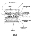
- Figure 1 of the accompanying drawings illustrates schematically the electrode arrangement of a single pixel whereas Figure 2 of the accompanying drawings illustrates the electrode arrangement of a small display panel of this type comprising rows and columns of pixels.
- the electrode arrangement comprises a plurality of first elongate electrodes such as 1 which are connected together for receiving a first data signal for controlling the state of the FLC below the first electrodes 1.
- Second elongate electrodes such as 2 are interdigitated with the first electrodes 1 and connected together so as to receive another data signal for controlling the optical state of the FLC below the second electrodes 2.
- the first and second electrodes extend along the columns of pixels and are common to the pixels such as 3 of each column.
- the first and second electrodes 1 and 2 are disposed on one side of the FLC (not shown) whereas third or row electrodes such as 4 are disposed on the other side of the FLC.
- the row electrodes 4 are connected to a strobe signal generator (not shown) for supplying a strobe signal in turn to the row electrodes 4. This arrangement forms a passive matrix addressing arrangement.
- first, second and third electrodes In order to control the optical state of each pixel, three independent connections are required to the first, second and third electrodes. when arranged as an array of pixels as shown in Figure 2, the third or row electrodes 4 are common to the pixels of each row and the first and second electrodes 1 and 2 are common to the pixels of each column.
- a data signal generator (not shown) supplies data signals to the first and second electrodes 1 and 2 of each column so that two data connections are required for each column of pixels, despite the fact that the pixels operate in either of two modes, namely diffractive and non-diffractive.
- the data signal generator is therefore required to have two line drivers per column of pixels and each column of pixels has to be provided with two connection pads for connection to the data signal generator.
- a spatial light modulator comprising at least three picture elements, each of which comprises a plurality of first elongate electrodes which are connected together and a plurality of second elongate electrodes which are connected together and which are interdigitated with the first electrodes, the first electrodes of a second of the picture elements being connected to the second electrodes of a first of the picture elements and the second electrodes of the second picture elements being connected to the first electrodes of a third of the picture elements.
- the interdigitated electrodes are shared between pixels so that the number of connections, and hence the number of line drivers, can be reduced compared with the known arrangement.
- the cost of a spatial light modulator for instance for use as a display panel, can also be reduced.
- the use of passive addressing techniques as opposed to active addressing techniques is intended to reduce costs because active substrates with associated fabrication costs and low yield can be avoided.
- the main cost of using the passive addressing technique is the number of independent drivers, for instance used to address columns and rows of pixels.
- the present invention allows the number of drivers to be approximately halved compared with the known technique described hereinbefore which results in a similar cost decrease. The cost advantage of passive addressing techniques over active techniques is thus maintained.
- Another advantage of this arrangement is in the reduction of electrode pads (pin-outs) which are required to allow connection, for instance, to silicon based drivers through chip-on-glass or similar techniques. Such pin-outs occupy area and can be disadvantageous from the point of view of overall panel size. The reduction in pin-outs also increases fabrication yield during manufacture.
- the modulator may comprise at least one row of n picture elements where n is an integer greater than 2, the first electrode of each ith picture element being connected to the second electrode of the (i-1)th picture element and the second electrode of each ith picture element being connected to the first electrode of the (i+1)th picture element, where i is each integer satisfying 1 ⁇ i ⁇ n.
- n is an integer greater than 2
- the present invention requires only n+1 pin-outs and drivers.
- the or each row may comprise a third electrode which is common to the n picture elements.
- Such an arrangement allows a passive matrix addressing technique to be employed.
- the modulator may comprise a plurality of columns of picture elements, the first electrodes of the picture elements of each column being connected together and the second electrodes of the picture elements of each column being connected together. This allows the whole modulator to be addressed as a single unit.
- the modulator may comprise a plurality of groups of rows of picture elements, each group comprising a plurality of columns of picture elements, the first electrodes of the picture elements of each column of each group being connected together and the second electrodes of the picture elements of each column of each group being connected together.
- the modulator is divided "horizontally" into several groups of rows (normally two) so that the groups can be addressed simultaneously. This reduces the frame refresh time of the modulator.
- the first and second electrodes may be connected to a data signal generator.
- the modulator may comprise an active matrix addressing arrangement connected to the first electrode of each of the picture elements.
- the modulator may include a layer of electro-optic material such as a liquid crystal, for instance a ferroelectric liquid crystal.
- the picture elements may be arranged as groups of m adjacent picture elements of different areas, where m is an integer greater than 1. This allows spatial techniques to be used for providing grey levels and is advantageous in the case where the pixels are switchable between two stable states.
- a display comprising a modulator in accordance with the first aspect of the invention, a light source for illuminating the modulator, and an optical system for gathering light from the modulator.
- the optical system may be arranged to gather light diffracted by the picture elements (pixels) of the modulator.
- pixels picture elements
- non-diffracting pixels appear dark whereas diffracting pixels appear light.
- Light from diffracting pixels which might contaminate the dark pixel image is thus reduced so that the display contrast ratio is increased.
- the optical system may be a projection optical system.
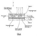
- FIGS 3 and 4 illustrate the structure of a pixel of a spatial light modulator (SLM) constituting an embodiment of the invention.
- the SLM constitutes a reflection-mode diffractive display panel comprising a rectangular array of rectangular or substantially rectangular pixels 3.
- the panel comprises upper and lower glass substrates 5 and 6.
- the upper substrate 5 is coated with a transparent conducting layer of indium tin oxide (ITO) which is etched to form the elongate interdigitated electrodes 1, 2 with a pattern as described hereinafter.
- the electrodes are covered with an alignment layer 7 for a ferroelectric liquid crystal material.
- ITO indium tin oxide
- the alignment layer 7 is formed by obliquely evaporating silicon oxide at 84° to the normal to the substrate 5 so as to induce the C1 state in a ferroelectric liquid crystal material, for instance of the type known as SCE8 available from Merck.
- the alignment layer 7 may have a thickness of approximately 10 nanometres.
- the third electrode 4 also forms a mirror and is formed on the glass substrate 6 by depositing silver to a thickness of approximately 100 nanometres.
- a static quarter wave plate 8 is formed on the silver mirror and electrode 4.
- the wave plate 8 may be provided by spinning on a mixture of reactive mesogen diacrylate RM257 in a suitable solvent such as toluene/xylene mix with a photoinitiator. This is cured for approximately 10 minutes under ultraviolet light in an atmosphere of nitrogen.
- the thickness of the plate 8 is controlled, for instance by varying the mix ratios of the materials and the spin speed, so that it acts as a quarter wave plate for a predetermined bandwidth in the visible spectrum, for instance, centred about 520 nanometres.
- the quarter wave plate 8 typically has a thickness of the order of 800 nanometres.
- a further alignment layer 9 is formed on the quarter wave plate 8, for instance as described hereinbefore for the alignment layer 7.
- the substrates 5 and 6 are then spaced apart, for instance by spacer balls of two micrometre diameter, and stuck together so as to form a cell which is filled with the ferroelectric liquid crystal material to form a layer 10.
- the spacing provides a layer of ferroelectric liquid crystal material which provides a half wave of retardation so that the liquid crystal layer 10 acts as a half wave retarder whose optic axis is switchable.
- the reflectivity of each interface should preferably be reduced, for instance by applying anti-reflection coatings to the substrate 5 and by optically burying the electrodes 1, 2.
- the layer 10 can be controlled so that the pixel is switched between diffractive and non-diffractive states.
- the FLC layer 10 In the non-diffractive state, the FLC layer 10 is in the same optical state throughout the pixel 3.
- the pixel 3 thus acts as a specular reflector.
- alternate strips of the FLC layer 10 as indicated at 11 and 12 are in different optical states such that light passing through each strip 11 is shifted in phase by 180° relative to light passing through each strip 12.
- the pixel 3 thus acts as a phase-only diffraction grating to unpolarised incident light, which is diffracted into the non-zero diffraction orders.
- Figure 5 illustrates the arrangement of the first, second and third electrodes 1, 2 and 4 of the SLM shown in Figures 3 and 4.
- a first pixel 3 comprises the first and second electrodes I and 2 with the same arrangement as illustrated in Figure 2.
- Second and third pixels 3' and 3" likewise comprise first electrodes 1' and 1" and second electrodes 2' and 2".
- the second electrodes 2 of the first pixel 3 are connected together and to the first electrodes 1' of the second pixel 3'.
- the second electrodes 2' of the second pixel 3' are connected together and to the first electrodes 1" of the third pixel 3".
- the first electrodes of each pixel column are connected together and to the second electrodes of the adjacent pixel column to the left whereas the second electrodes of each pixel column are connected together and to the first electrodes of the adjacent pixel column to the right.
- the first electrodes are not connected to other electrodes but the second electrodes are connected to the first electrodes of the next column.
- the right-most column has second electrodes which are not connected to another column and first electrodes which are connected to the second electrodes of the adjacent column.
- Figure 6 illustrates a projection display using an SLM 14 of the type shown in Figures 3 to 5.
- the SLM 14 is illuminated by a light source 15.
- Projection lenses 16 and 17 and mirrors 18 and 19 project an image displayed by the SLM 14 onto a screen 20.
- Each pixel which is in the reflective mode reflects the incident light normally back so that the reflected light is not projected by the optical elements 16 to 19. Thus, a "dark" pixel is imaged on the screen 20.
- Each pixel in the diffractive mode deflects the incident light into the non-zero diffractive orders, mainly into the positive and negative first orders as illustrated by light rays 21 and 22. The light from each such pixel is thus imaged to a "bright" pixel on the screen 20.
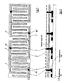
- Figure 7 illustrates an electrode arrangement and addressing circuitry of an SLM which is divided at a panel split line 24 into two substantially identical panels.
- the first and second electrodes 1, 2 are connected to an upper data signal generator 25 and a lower data signal generator 26 for the upper and lower halves of the panel.
- the strobe electrodes 4 are similarly connected to upper and lower strobe signal generators 27 and 28.
- the data and strobe signal generators 25 to 28 form the addressing circuitry for the whole panel relative to the upper and lower halves of the panel which are substantially independent of each other.
- these halves are addressed as two separate panels with each being addressed one row at a time. Accordingly, the frame refresh period of the whole panel may be halved or the line address time may be doubled.
- first and second electrodes 1, 2 shown in Figure 7 The layout for the first and second electrodes 1, 2 shown in Figure 7 is such that these electrodes can be contained within a single plane. This avoids the need for double layer lithography to create the electrode pattern in two layers with interconnections where necessary between the layers.
- each half of the panel is electrically asymmetrical. For instance, the electrodes connected to the conductor 29 are connected with a short conductive path to the data signal generator 25 whereas the electrodes connected to the conductor 30 are connected via a higher resistance path.
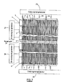
- Figure 8 illustrates the technique required for addressing an SLM panel of the type shown in Figure 7.
- the strobe pulses are represented by the "0s" and "1s" indicated at 31, where a "1" represents a strobe pulse being applied to a strobe electrode for refreshing a row of pixels.
- the panel shown in Figure 8 comprises 3 upper rows and 3 lower rows with the middle row of each half of the panel being strobed.
- the data signals which are simultaneously applied to the first and second electrodes in synchronism with the strobe pulses are also illustrated by "0s" and "1s” as shown as 32 and 33.
- "0" represents a first voltage for switching the strips of FLC to a first optical state
- "1" represents the second voltage for switching the strips of FLC to a second optical state.
- the pixel is in the non-diffractive state irrespective of which optical state the strips are in.
- the pixel is switched to the diffractive state irrespective of which voltages are applied to which of the first and second electrodes. Accordingly, the pixels are switched to the diffractive state where adjacent electrodes are connected to different voltages. This is indicated, for instance at 34, by a white region whereas non-diffractive pixels are indicated by shaded regions such as 35.
- each pixel is either bright or dark with no other grey levels being available.
- the individual pixels may be grouped together and operated in such a way as to provide what is known as "spatial dither".
- spatial dither By appropriately selecting the layout of the first and second electrodes, the individual pixels of each group forming a composite pixel can have different areas, for instance increasing logarithmically from the smallest to the largest with the areas of adjacent pixels being in the ratio of 2:1.
- spatial resolution may be sacrificed in order to provide grey level capability.
- Electrodes represented by unbroken lines such as 42 form one layer whereas electrodes indicated by broken lines 43 form another layer.
- Such an arrangement allows electrical symmetry to be achieved between the electrodes but requires a two level arrangement with interconnections between the levels, for instance to the data signal generators.
- the actual strobe and data waveforms may be those which are conventionally used for addressing ferroelectric liquid crystal displays.
- Such techniques are disclosed in "The JOERS/ALVEY Ferroelectric Multi-Plexing Scheme", P.W.H. Surguy et al, Ferroelectrics 122 pp 63-79 (1991) and in "A New Set of High Speed Matrix Addressing Schemes for Ferroelectric Liquid Crystal Displays", J.R. Hughes and E.P. Raynes, Liq.Cryst. 13 pp 597-601, 1993.
- Waveforms suitable for use with the panels and pixels shown in Figures 3 to 8 of the JOERS/ALVEY type are illustrated in Figure 9.
- Each of the strobe signals comprises a blanking pulse 45 followed by a strobe pulse 46 of opposite polarity, larger amplitude and shorter duration.
- the data waveforms are illustrated at 47 and comprise contiguous pulses of equal amplitude but opposite polarity, each pulse having the same period as the strobe pulses 46.
- the right hand side of Figure 9 illustrates the combinations of strobe and data pulses for switching the pixels to the diffractive state "ON" or for leaving the pixels in the blanked non-diffractive state "OFF".
- Figure 10 illustrates at (a) to (d) the four possible states of a typical pixel 3' and the effect on the adjacent pixels 3 and 3".
- Non-diffracting states are shown at (a) and (b) whereas diffracting states are shown at (c) and (d).
- all of the strips of the pixel 3' are in the state 11. Because of the interconnections of the electrodes with the adjacent pixels, alternate strips of the pixel 3 and of the pixel 3" are in the state 11. However, the remaining strips such as 50 and 51 of the pixels 3 and 3" can be in any arbitrary state so that the pixels 3 and 3" may be controlled so as to be diffracting or non-diffracting in respective of the specific state of the pixel 3' shown at (a).
- the other non-diffracting state of the pixel 3' is shown at (b).
- all of the strips of the pixel 3' are in the state 12 as are alternate strips of the adjacent pixels 3 and 3".
- the remaining strips such as 50 and 51 of the pixels 3 and 3" can be in either state so that the pixels 3 and 3" maybe diffracting or non-diffracting as desired and irrespective of the state of the pixel 3'.
- alternate strips of the pixel 3' are in different states 11 and 12.
- alternate strips of the pixel 3 are in the state 11 whereas alternate strips of the pixel 3" are in the state 12.
- the remaining strips 50 and 51 of the pixels 3 and 3" maybe in either state so that the states of the pixels 3 and 3" maybe selected in independently and irrespective of the state of the pixel 3'.
- the states of the strips of the pixel 3' are reversed compared with the states illustrated at (c) but again the adjacent pixels 3 and 3" may be controlled to be in either state as desired and irrespective of the state of the pixel 3'. Accordingly, all of the pixels are independently controllable despite the reduction in the number of connections required by the "electrode sharing" arrangement.
- FIG. 5 and 7 to 9 are of the passive matrix addressing type.
- active matrix addressing may also be used with a shared electrode arrangement for pixels of the type illustrated in Figures 3 and 4.
- Figure 11 illustrates the intedigitated electrode arrangement for an active matrix SLM.
- the second electrode 2 of the pixel 3 is connected to the first electrode 1' of the adjacent pixel 3'.
- the second electrode 2' of the pixel 3' is connected to the first electrode 1" of the adjacent pixel 3".
- only a single via connection is required for the indigitated first and second electrodes at each pixel.
- the number of connections is reduced by approximately 50%.
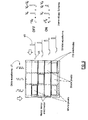
- FIG 12 illustrates an active matrix addressing substrate in simplified form.
- the substrate comprises a thin film transistor (TFT) back plane 56 on which is formed a mirror layer 57 which may be metallic or dielectric.
- the via connections such as 55 extend through the layer 57 so as to provide a connection between the interdigitated electrodes and the back plane 56.
- the electrodes such as 1 and 2 are formed above the layer 57.
- the facing substrate (not shown) carries a transparent continuous third electrode which is common to all of the pixels of the modulator.
- the waveforms appearing across the strips of FLC in each pixel are DC balanced.
- Accurate balancing can be provided by applying each frame of data twice with the data and strobe waveforms having inverted polarity during the second frame.
- Adequate results can be achieved by inverting the polarities of the strobe and data waveforms periodically, for instance after each frame of data.
- ferroelectric liquid crystals other liquid crystal materials may be used, such as nematic liquid crystals, anti-ferroelectric liquid crystals (AFLC) and particularly highly twisted non-linear material structures such as super twisted nematic (STN) materials. Also, these techniques may be applied to non liquid crystal embodiments and even to non-electrooptic embodiments, such as grating light valves (GLVs) as disclosed in “Deformable Grating Light Valves for High-Resolution Displays", Apte et al, SID 1993, pp 807-8.
- GLVs grating light valves
- each pixel has electrodes shared between adjacent nodes (i.e. thin film transistors) of the addressing architecture.
- AFLC modes may also be used with active matrix addressing.
- the ideal AFLC mode requires a threshold less AFLC in which the voltage-transmission relationship does not exhibit the typical hysteretic loop.
- Binary (on/off) or analogue (grey level) operation may be provided in this mode.
- a modulator of the type described hereinbefore may also be embodied using a bistable twisted nematic (BTN) liquid crystal in an active matrix addressing arrangement.
- BTN bistable twisted nematic
- a cholesteric doped nematic liquid crystal material having a pitch of approximately twice the cell gap in an anti-parallel aligned cell produces a splayed 180° twist state and two splayed metastable states with 0° and 360° twist.
- the two metastable states provide a bistable mode of operation for the liquid crystal.
- the liquid crystal can be switched between the metastable states by applying a reset pulse, which produces a temporary homeotropic state, followed by a select pulse to select one of the two metastable states.
- the metastable states may be rapidly accessed and represent the bistable states.
- the BTN mode can operate in other ways, for instance with passive matrix addressing and in the analogue mode to provide grey levels. Also, other BTN configurations may be used.
Landscapes
- Physics & Mathematics (AREA)
- Nonlinear Science (AREA)
- General Physics & Mathematics (AREA)
- Optics & Photonics (AREA)
- Geometry (AREA)
- Mathematical Physics (AREA)
- Chemical & Material Sciences (AREA)
- Crystallography & Structural Chemistry (AREA)
- Liquid Crystal (AREA)
Applications Claiming Priority (2)
| Application Number | Priority Date | Filing Date | Title |
|---|---|---|---|
| GB9716112A GB2327797A (en) | 1997-07-31 | 1997-07-31 | Spatial light modulator and display |
| GB9716112 | 1997-07-31 |
Publications (2)
| Publication Number | Publication Date |
|---|---|
| EP0899606A2 true EP0899606A2 (de) | 1999-03-03 |
| EP0899606A3 EP0899606A3 (de) | 1999-12-22 |
Family
ID=10816717
Family Applications (1)
| Application Number | Title | Priority Date | Filing Date |
|---|---|---|---|
| EP98306024A Withdrawn EP0899606A3 (de) | 1997-07-31 | 1998-07-29 | Räumlicher Lichtmodulator und Anzeigevorrichtung |
Country Status (4)
| Country | Link |
|---|---|
| US (1) | US6094249A (de) |
| EP (1) | EP0899606A3 (de) |
| JP (1) | JP3922498B2 (de) |
| GB (1) | GB2327797A (de) |
Cited By (3)
| Publication number | Priority date | Publication date | Assignee | Title |
|---|---|---|---|---|
| WO2002079870A2 (en) * | 2001-03-28 | 2002-10-10 | Thomas Swan & Co. Ltd. | Device and method for steering a beam of light |
| WO2003044763A1 (en) * | 2001-11-22 | 2003-05-30 | Koninklijke Philips Electronics N.V. | Bistable liquid crystal device having two drive modes |
| WO2004107029A1 (en) * | 2003-06-02 | 2004-12-09 | Cambridge University Technical Services Limited | Liquid crystal device |
Families Citing this family (15)
| Publication number | Priority date | Publication date | Assignee | Title |
|---|---|---|---|---|
| US6707519B1 (en) | 1998-02-04 | 2004-03-16 | Seiko Epson Corporation | Three state transflective liquid crystal display |
| DE19815337C2 (de) * | 1998-04-06 | 2001-07-05 | Deutsche Telekom Ag | Vorrichtung zur lokalen Abschwächung der Lichtintensität im Sehfeld einer lichtempfindlichen Beobachtungseinrichtung |
| GB2341476A (en) * | 1998-09-03 | 2000-03-15 | Sharp Kk | Variable resolution display device |
| GB2345978A (en) * | 1999-01-23 | 2000-07-26 | Sharp Kk | Diffractive spatial light modulator |
| US6630982B2 (en) * | 2001-10-18 | 2003-10-07 | Motorola, Inc. | Color and intensity tunable liquid crystal device |
| IL152029A0 (en) * | 2002-09-30 | 2003-04-10 | Magink Display Technologies | Distinct color lcd apparatus |
| KR100459409B1 (ko) * | 2002-10-24 | 2004-12-03 | 엘지전자 주식회사 | 공간 광 모듈레이터 및 그 제조방법 |
| KR100459408B1 (ko) * | 2002-10-24 | 2004-12-03 | 엘지전자 주식회사 | 레이저 디스플레이용 공간 광 모듈레이터 소자 및 그제조방법 |
| KR100459410B1 (ko) * | 2002-10-31 | 2004-12-03 | 엘지전자 주식회사 | 광모듈레이터 소자 및 생산방법 |
| ATE419613T1 (de) * | 2004-11-10 | 2009-01-15 | Magink Display Technologies | Ansteuerschema für ein cholesterisches flüssigkristallanzeigebauelement |
| US7359105B2 (en) * | 2006-02-07 | 2008-04-15 | Sharp Kabushiki Kaisha | Spatial light modulator and a display device |
| JP5214509B2 (ja) * | 2008-03-24 | 2013-06-19 | シチズンホールディングス株式会社 | 光変調装置 |
| KR101704738B1 (ko) * | 2010-07-26 | 2017-02-08 | 한국전자통신연구원 | 고해상도 홀로그래픽 디스플레이 |
| WO2017006789A1 (ja) * | 2015-07-03 | 2017-01-12 | シャープ株式会社 | 液晶表示装置 |
| WO2022057738A1 (en) * | 2020-09-21 | 2022-03-24 | The Hong Kong University Of Science And Technology | High-contrast ferroelectric liquid crystal cell |
Citations (2)
| Publication number | Priority date | Publication date | Assignee | Title |
|---|---|---|---|---|
| US4902103A (en) * | 1987-08-10 | 1990-02-20 | Koito Manufacturing Co., Ltd. | Color liquid-crystal display unit with electrodes interleaved in vertical and horizontal directions |
| EP0501824A2 (de) * | 1991-02-28 | 1992-09-02 | Raytheon Company | Optischer Strahlablenker mit Adressierung durch unterteilte Öffnungen |
Family Cites Families (11)
| Publication number | Priority date | Publication date | Assignee | Title |
|---|---|---|---|---|
| US3609002A (en) * | 1969-12-30 | 1971-09-28 | Bell Telephone Labor Inc | Multiple element optical memory structures using fine grain ferroelectric ceramics |
| US3781080A (en) * | 1972-11-30 | 1973-12-25 | Gen Electric | Liquid crystal device for generating reticles in optical equipment |
| US3981559A (en) * | 1974-11-25 | 1976-09-21 | Rca Corporation | Liquid crystal display |
| CA1197638A (en) * | 1980-07-03 | 1985-12-03 | Control Interface Company Limited | Field sensitive optical displays, generation of fields therefor and scanning thereof |
| JPS63229430A (ja) * | 1987-03-18 | 1988-09-26 | Nec Corp | 液晶デイスプレイ |
| JPH04174417A (ja) * | 1990-11-07 | 1992-06-22 | Sharp Corp | カラー液晶表示装置 |
| KR100367869B1 (ko) * | 1993-09-20 | 2003-06-09 | 가부시끼가이샤 히다치 세이사꾸쇼 | 액정표시장치 |
| TW289097B (de) * | 1994-08-24 | 1996-10-21 | Hitachi Ltd | |
| GB2313920A (en) * | 1996-06-07 | 1997-12-10 | Sharp Kk | Diffractive spatial light modulator and display |
| KR100250796B1 (ko) * | 1996-11-29 | 2000-04-01 | 김영환 | 액정 표시 소자 및 그 제조방법 |
| US5991065A (en) * | 1996-12-10 | 1999-11-23 | Eastman Kodak Company | Addressable electro-optic modulator with periodically poled domain regions |
-
1997
- 1997-07-31 GB GB9716112A patent/GB2327797A/en not_active Withdrawn
-
1998
- 1998-07-28 JP JP21319298A patent/JP3922498B2/ja not_active Expired - Fee Related
- 1998-07-29 US US09/124,655 patent/US6094249A/en not_active Expired - Fee Related
- 1998-07-29 EP EP98306024A patent/EP0899606A3/de not_active Withdrawn
Patent Citations (2)
| Publication number | Priority date | Publication date | Assignee | Title |
|---|---|---|---|---|
| US4902103A (en) * | 1987-08-10 | 1990-02-20 | Koito Manufacturing Co., Ltd. | Color liquid-crystal display unit with electrodes interleaved in vertical and horizontal directions |
| EP0501824A2 (de) * | 1991-02-28 | 1992-09-02 | Raytheon Company | Optischer Strahlablenker mit Adressierung durch unterteilte Öffnungen |
Cited By (5)
| Publication number | Priority date | Publication date | Assignee | Title |
|---|---|---|---|---|
| WO2002079870A2 (en) * | 2001-03-28 | 2002-10-10 | Thomas Swan & Co. Ltd. | Device and method for steering a beam of light |
| WO2002079870A3 (en) * | 2001-03-28 | 2003-01-03 | Swan Thomas & Co Ltd | Device and method for steering a beam of light |
| US7417706B2 (en) | 2001-03-28 | 2008-08-26 | Thomas Swan And Co. Ltd. | Beam steering device |
| WO2003044763A1 (en) * | 2001-11-22 | 2003-05-30 | Koninklijke Philips Electronics N.V. | Bistable liquid crystal device having two drive modes |
| WO2004107029A1 (en) * | 2003-06-02 | 2004-12-09 | Cambridge University Technical Services Limited | Liquid crystal device |
Also Published As
| Publication number | Publication date |
|---|---|
| GB9716112D0 (en) | 1997-10-08 |
| GB2327797A (en) | 1999-02-03 |
| US6094249A (en) | 2000-07-25 |
| JP3922498B2 (ja) | 2007-05-30 |
| EP0899606A3 (de) | 1999-12-22 |
| JPH1195240A (ja) | 1999-04-09 |
Similar Documents
| Publication | Publication Date | Title |
|---|---|---|
| US6281866B1 (en) | Display device and a method of addressing a display device | |
| US6243063B1 (en) | Diffractive spatial light modulator and display | |
| US6094249A (en) | Spatial light modulator and display with reduced electrical connectivity requirement | |
| US6201589B1 (en) | Spatial light modulator and display with picture elements having electrically floating electrodes | |
| US8552925B2 (en) | Stereoscopic image display apparatus | |
| CN1020232C (zh) | 一种液晶显示器件及其驱动方法 | |
| US20050225545A1 (en) | Liquid crystal display apparatus and method of driving the same | |
| KR100300280B1 (ko) | 액티브 매트릭스 광 변조기 및 표시 장치 | |
| JP3596716B2 (ja) | アクティブマトリクス型表示装置の調整方法 | |
| GB2325056A (en) | Polarisation independent optical phase modulator | |
| US6104368A (en) | Diffractive liquid crystal device | |
| US5898416A (en) | Display device | |
| US9250460B2 (en) | Liquid crystal display comprising erase electrodes | |
| US20020149552A1 (en) | Bistable chiral nematic liquid crystal display and method of driving the same | |
| JP3713922B2 (ja) | 液晶表示装置の駆動装置、液晶表示装置、電子機器、及び液晶表示装置の駆動方法 | |
| CN1129806C (zh) | 铁电液晶显示器 | |
| JPH08328046A (ja) | 反強誘電性液晶表示素子 | |
| GB2293260A (en) | Liquid crystal device |
Legal Events
| Date | Code | Title | Description |
|---|---|---|---|
| PUAI | Public reference made under article 153(3) epc to a published international application that has entered the european phase |
Free format text: ORIGINAL CODE: 0009012 |
|
| AK | Designated contracting states |
Kind code of ref document: A2 Designated state(s): DE FR GB |
|
| AX | Request for extension of the european patent |
Free format text: AL;LT;LV;MK;RO;SI |
|
| PUAL | Search report despatched |
Free format text: ORIGINAL CODE: 0009013 |
|
| AK | Designated contracting states |
Kind code of ref document: A3 Designated state(s): AT BE CH CY DE DK ES FI FR GB GR IE IT LI LU MC NL PT SE |
|
| AX | Request for extension of the european patent |
Free format text: AL;LT;LV;MK;RO;SI |
|
| 17P | Request for examination filed |
Effective date: 20000511 |
|
| AKX | Designation fees paid |
Free format text: DE FR GB |
|
| GRAP | Despatch of communication of intention to grant a patent |
Free format text: ORIGINAL CODE: EPIDOSNIGR1 |
|
| STAA | Information on the status of an ep patent application or granted ep patent |
Free format text: STATUS: THE APPLICATION IS DEEMED TO BE WITHDRAWN |
|
| 18D | Application deemed to be withdrawn |
Effective date: 20070303 |