EP0501570A1 - Digitales Regelsystem sowie Teilschaltung zur Anordnung im Regelsystem - Google Patents
Digitales Regelsystem sowie Teilschaltung zur Anordnung im Regelsystem Download PDFInfo
- Publication number
- EP0501570A1 EP0501570A1 EP92200478A EP92200478A EP0501570A1 EP 0501570 A1 EP0501570 A1 EP 0501570A1 EP 92200478 A EP92200478 A EP 92200478A EP 92200478 A EP92200478 A EP 92200478A EP 0501570 A1 EP0501570 A1 EP 0501570A1
- Authority
- EP
- European Patent Office
- Prior art keywords
- circuit
- sub
- input
- series
- output
- Prior art date
- Legal status (The legal status is an assumption and is not a legal conclusion. Google has not performed a legal analysis and makes no representation as to the accuracy of the status listed.)
- Granted
Links
- 238000000034 method Methods 0.000 claims description 2
- 238000013139 quantization Methods 0.000 abstract description 4
- 230000005855 radiation Effects 0.000 description 14
- 238000001228 spectrum Methods 0.000 description 12
- 230000003287 optical effect Effects 0.000 description 9
- 238000010606 normalization Methods 0.000 description 6
- 238000010586 diagram Methods 0.000 description 2
- 230000000694 effects Effects 0.000 description 2
- FFBHFFJDDLITSX-UHFFFAOYSA-N benzyl N-[2-hydroxy-4-(3-oxomorpholin-4-yl)phenyl]carbamate Chemical compound OC1=C(NC(=O)OCC2=CC=CC=C2)C=CC(=C1)N1CCOCC1=O FFBHFFJDDLITSX-UHFFFAOYSA-N 0.000 description 1
- 230000007423 decrease Effects 0.000 description 1
- 230000001627 detrimental effect Effects 0.000 description 1
- 230000002349 favourable effect Effects 0.000 description 1
- 230000017525 heat dissipation Effects 0.000 description 1
- 238000009877 rendering Methods 0.000 description 1
- 230000001360 synchronised effect Effects 0.000 description 1
Images


Classifications
-
- G—PHYSICS
- G05—CONTROLLING; REGULATING
- G05B—CONTROL OR REGULATING SYSTEMS IN GENERAL; FUNCTIONAL ELEMENTS OF SUCH SYSTEMS; MONITORING OR TESTING ARRANGEMENTS FOR SUCH SYSTEMS OR ELEMENTS
- G05B13/00—Adaptive control systems, i.e. systems automatically adjusting themselves to have a performance which is optimum according to some preassigned criterion
-
- G—PHYSICS
- G11—INFORMATION STORAGE
- G11B—INFORMATION STORAGE BASED ON RELATIVE MOVEMENT BETWEEN RECORD CARRIER AND TRANSDUCER
- G11B7/00—Recording or reproducing by optical means, e.g. recording using a thermal beam of optical radiation by modifying optical properties or the physical structure, reproducing using an optical beam at lower power by sensing optical properties; Record carriers therefor
- G11B7/08—Disposition or mounting of heads or light sources relatively to record carriers
- G11B7/09—Disposition or mounting of heads or light sources relatively to record carriers with provision for moving the light beam or focus plane for the purpose of maintaining alignment of the light beam relative to the record carrier during transducing operation, e.g. to compensate for surface irregularities of the latter or for track following
- G11B7/094—Methods and circuits for servo offset compensation
-
- G—PHYSICS
- G11—INFORMATION STORAGE
- G11B—INFORMATION STORAGE BASED ON RELATIVE MOVEMENT BETWEEN RECORD CARRIER AND TRANSDUCER
- G11B7/00—Recording or reproducing by optical means, e.g. recording using a thermal beam of optical radiation by modifying optical properties or the physical structure, reproducing using an optical beam at lower power by sensing optical properties; Record carriers therefor
- G11B7/08—Disposition or mounting of heads or light sources relatively to record carriers
- G11B7/09—Disposition or mounting of heads or light sources relatively to record carriers with provision for moving the light beam or focus plane for the purpose of maintaining alignment of the light beam relative to the record carrier during transducing operation, e.g. to compensate for surface irregularities of the latter or for track following
- G11B7/0941—Methods and circuits for servo gain or phase compensation during operation
Definitions
- the invention relates to a digital control system, comprising an actuator for influencing a state variable in a process, a sensor for detecting the state variable, a converter for converting the detected state variable into a series of digital measured signal values, a digital signal processor for deriving an actuator control signal from the series of measured signal values.
- the invention further relates to a digital sub-circuit to be used in the digital servo system.
- a digital control system is known, for example, from European Patent Application 0 390 467.
- the digital control system described in that document relates to the focus control and tracking control in an optical recording and/or reproducing apparatus, in which an optical record carrier is detected with the aid of a radiation beam for recording and/or reproducing purposes.
- the focus error signal and the tracking error signal are then derived from the radiation beam reflected by the record carrier.
- the magnitude of the focus error signal and the tracking error signal is strongly related to the intensity of the radiation beam. This intensity strongly depends on the intensity of the radiation source used and on the reflection of the record carrier. Since these parameters may vary considerably there is a need for rendering the loop gain of the control system electronically adjustable and/or normalizing the error signals by dividing the focus error signal by the intensity of the detected radiation beam.
- Optical recording and/or reproducing apparatus in which the normalization and/or adjustable gain are realised by means of analog multiplication and sub-circuits are known.
- optical recording and/or reproducing apparatus having digital focus and tracking controls there is a problem that digital multiplier circuits and/or digital sub-circuits are necessary for gain adjustment and/or normalization in digital control loops.
- the prior art digital multiplier circuits and the digital sub-circuits are disadvantageous in that they need very many components. This is especially a disadvantage in integrated circuits because these large amounts of components cover a relatively large chip surface which has a detrimental effect on the cost price of such an integrated circuit.
- the signal processor comprises a digital sub-circuit which has a first input for receiving a series of m-bit signal values which are related to the measured signal values, a second input for receiving an n-bit signal value and an output for producing a series of p-bit signal values which are indicative of the quotient of the series of m-bit signal values on the first input and the signal value on the second input, the signal processor also including a generating means for generating a control signal related to the series of signal values at the output of the sub-circuit, the sub-circuit including a multiplier which has a first input coupled to the output of the sub-circuit and a second input coupled to the second input of the sub-circuit and has an output for producing a series of signal values indicative of the product of the output signals and the signal samples on the second input, the multiplier output being coupled to a first input of a comparing circuit, a second input of the comparing circuit being coupled to the first
- the output signal is adapted in such a way that the low-frequency component in the series of signal values at the output of the multiplier is maintained equal to the low-frequency component in the series of signal values at the first input. That is to say, the low-frequency component of the output signal is equal to the quotient of the series of signal values at the first input and the signal value at the second input. Since the number of bits of the signal values at the output of the sub-circuit is small due to the quantization, a multiplier can be used having relatively few components. For that matter, the number of components required in a digital multiplier is strongly related to the number of bits of the signal values to be multiplied.
- the series of signal values at the output of the sub-circuit will be strongly affected by noise.
- the noise power will mainly be situated in the high-frequency portion of the spectrum of the series of signal values at the output.
- the noise component power in the low-frequency spectrum will then be negligibly small relative to the signal power in this low-frequency portion of this spectrum. This means that the noise resulting from the quantization can be cancelled without any problem without affecting the low-frequency component in the sub-circuit output signal.
- the sub-circuit comprises a negative feedback system. This implies that the sub-circuit may be brought from a stable to an unstable state when sign inversion of the signal value occurs at the second input. For that matter, sign inversion changes the negative feedback into an unstable positive feedback. This implies that the sub-circuit cannot be used in an unqualified manner for any signal value on the second input.
- This objection can be met by means of an embodiment of the invention characterized in that the output of the quantizing circuit is coupled to the output of the sub-circuit by means of a circuit for inverting the sign of the signal samples produced by the quatizing circuit in response to the sign of the signal samples on the second input.
- An extremely simple multiplier may be used in the case where the quantizing circuit converts the signal on its input into a 1-bit signal value. In that case a 1-bit multiplier will be sufficient.
- a further embodiment of the control system according to the invention is characterized in that the output of the sub-circuit is coupled to the input of the actuator only over an analog signal path.
- the output signal of the sub-circuit may be used directly for driving the actuator so that no additional digital-to-analog converter is necessary.
- the output of the sub-circuit is preferably connected to the actuator through a low-pass filter.
- the digital sub-circuit is pre-eminently suitable for use in control systems. However, the use of the digital sub-circuit is not restricted to control systems.
- the sub-circuit may, in essence, be used always when a series of digital signal values is to be divided by an adjustable devisor, like, for example, for the normalization of digitized audio and/or video signals.
- Fig. 1 shows a general block diagram of a digital control system according to the invention.
- the control system comprises a process 1 whose state variable, for example, a position of an object, may be influenced by an actuator 2.
- a sensor 3 detects the value of this state variable and the converter 4 converts the detected value of the state variable into a series of digital measured signal values I(k).
- a digital signal processor 5 derives a control signal Vs for the actuator 2 from the series of measured signal values I(k) according to a specific control criterion.
- the digital controller 5 comprises a digital sub-circuit 6.
- the digital sub-circuit 6 has an input 7 for receiving a series of n-bit signal values a(k) related to the series of digital measured signal values I(k) produced by the converter 4.
- the sub-circuit 6 has a further input 8 for receiving an n-bit signal value b.
- the sub-circuit has an output 9 at which a series of p-bit output signal values I(k) are produced which are indicative of the quotient a(k)/b of the series of signal values a(k) on the input 7 and the signal value b on the input 8.
- Fig. 2a shows a first embodiment of the digital sub-circuit 6.
- This sub-circuit comprises a multiplier 20 whose inputs are connected to the output 9 and input 8 respectively.
- the output of the multiplier 20 is coupled, for example, by means of an m-bit data bus 22, to one of the inputs of a comparing circuit 21.
- a further input of the comparing circuit 21 is coupled to the input 7 of the sub-circuit 6.
- the comparing circuit 21 produces a series of m-bit signal values indicative of the difference e(k) between a series of m-bit signal values a(k) at input 7 and the series of m-bit signal values at the output of the multiplier 20.
- the series of digital signal values e(k) are applied to a digital integral-action filter 24.
- a filter of this type may be a first-order or higher-order filter.
- Fig. 8 shows an embodiment of a first-order integral-action filter.
- This filter comprises a delay element 80, for example, a synchronous register controlled with sample frequency fs.
- the output of the delay element 80 is fed back to a first input of an adder circuit 81.
- a second input of the adder circuit 81 operates as the input to the filter 24, whereas the output of the delay element operates as the output of the filter 24.
- the filter 24 produces a series of multi-bit signal values ⁇ e(k), for example, 12-bit signals, which are indicative of a summation of the series of signal values received at the input.
- the series of signal values ⁇ e(k) at the output of the filter 24 is applied to a quantizing circuit 25, for example, over an m-bit data bus 26.
- the quantizing circuit 25 is a circuit of a customary type, converting the m-bit signal values into p-bit signal values.
- the quantizing circuit 25 may comprise, for example, a circuit separating the p most significant bits from the signal values applied to the input.
- the p-bit signal values represented by these p bits are applied to the input 9 of the sub-circuit 6.
- the sub-circuit 6 forms a negative feedback system which has a low-frequency response curve owing to the integral-action filter 24.
- the low-frequency content of the series of signal values b.o(k) is equal to the low-frequency content of the series of signal values a(k). This denotes that the low-frequency content of the series of signal values o(k) is equal to the low-frequency content of the quotient a(k)/b.
- the noise power P(r) in the series of signal values o(k) will be large.
- the bandwidth of the control loop is much smaller than the sample frequency fs, the noise power is especially concentrated in the high-frequency region of the spectrum of the series of signal values o(k).
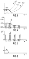
- Fig. 3 shows by way of illustration a customary transfer characteristic Hs of a control system plotted against frequency f.
- the bandwidth which is, for example, 2 kHz, is referenced Bl.
- Fig. 3 furthermore shows the noise power Pr, Pr' and Pr'' of the series o(k) depicted as functions of the frequency f for the respective sample frequencies fs, fs' and fs'', where fs>fs'>fs''.
- Fig. 3 proves that the portion of the noise power Pr within the bandwidth Bl of the control system decreases according as the sample frequency increases.
- Fig. 4 shows as an illustrative example a series of 12-bit signal values a(k) plotted against k.
- the values of a(k) are represented in the octal number system.
- Fig. 6 shows a possible spectrum Ha of the series a(k) plotted against frequency f.
- Fig. 7 shows the spectrum of the series of signal values o(k).
- the spectrum of Fig. 7 shows a low-frequency portion Hol which is equal to the spectrum Ha divided by the value b.
- the spectrum comprises the noise component Pr which is situated, in essence, outside the region of the spectrum covered by the low-frequency component Hol.
- the sub-circuit 6 forms a negative feedback system. This denotes that the necessary stability requirements are to be satisfied for a proper functioning. For the sub-circuit 6 shown in Fig. 2a this means that this circuit can only operate in a stable state for positive values of b on the input 8. Sign inversion of b will denote that the negative feedback changes into an unstable positive feedback.
- Fig. 2b shows an embodiment of the sub-circuit 6 in which the problem of instability is solved by inserting between the quantizing circuit 25 and the output 9 a circuit 27 which, in response to a signal sign.b which is indicative of the sign of the value of b, conveys in inverted fashion or not the signal value at the output of the quantizing circuit 25 to the output 9.
- the circuit 27 may comprise, for example, a controllable inverter circuit of a customary type. When using circuit 27 it is achieved that a sign inversion of the signal value b does not have any effect on the negative feedback, and thus not any effect on the stability of the sub-circuit 6.
- the number of bits per signal value produced by the quantizing circuit 25 is preferably small.
- the complexity of the multiplier 20 is strongly related to the number of bits of the signal values on its input.
- An extremely simple multiplier 20 may be used if the number of bits per signal value at the output is equal to 1. In that case AND gates may be used for the multiplier, which apply or do not apply the signal value b to the comparing circuit 21 in response to the logic value of the 1-bit signal values at the output 9.
- FIG. 9 shows a focus control included in such an optical recording and/or reproducing apparatus.
- reference number 90 denotes an optical record carrier of a customary type rotating around its axis 91.
- Opposite to the rotating record carrier 90 is installed an optical read and/or write head 92 of a customary type.
- the head 92 comprises a radiation source for generating a radiation beam 100 which is focused at a reflecting information layer 97 of the record carrier 90 through an objective 93, a semi-transparent mirror 94 and a focus objective 95.
- the radiation beam reflected by the record carrier 90 is pointed at a radiation-sensitive sensor 99 through the semi-transparent mirror 94 and a beam splitter 98, for example, a pentagonal prism. At that point the beam 100 is split into two sub-beams 100a and 100b by the beam splitter 98.
- the sensor 99 comprises a bank of four radiation-sensitive detectors 99a, 99b, 99c and 99d.
- the positions of the detectors 99a, ..., 99d is such that if the radiation beam 100 is focused on the information layer 97, the meeting surface of the beam 100a on the sensor 99 has a symmetrical position relative to the middle between the detectors 99a and 99b, whereas the meeting surface of the sub-beam 100b has a symmetrical position relative to the detectors 99c and 99d.
- the detectors 99a, ..., 99d produce four signal currents Ia, ..., Id which are indicative of the radiation power detected by the associated detectors.
- a focus error signal Fe indicative of the distance between the focal point of the beam 100 and the information layer 97 may be derived from the signal currents according to the following formula:
- the focus error signal Fe is normalized by the division of the differences (Ia - Ib) and (Ic - Id) by the respective sum values (Ia + Ib) and (Ic + Id). This normalization has rendered the focus error signal Fe independent of variations in the intensity of the reflected radiation beam.
- the signal currents Ia, Ib, Ic and Id are converted into series of digital signal values Ia(k), Ib(k), Ic(k) and Id(k) by the converter 4 and applied to digital signal processor 5.
- the signal processor derives therefrom a control signal Vs for an actuator 101 for shifting the focusing objective 95 in a direction denoted by an arrow 102 so that the radiation beam 100 is maintained in a position focused at the information layer 97.
- Fig. 10 shows in greater detail the focus control system shown in Fig. 9.
- the converter 4 comprises four analog-to-digital converters which include, for example, sigma-delta modulators, for converting the signal currents Ia, Ib, Ic and Id into series of digitized signal values Ia(k), Ib(k), Ic(k) and Id(k).
- the series of signal values I2(k) and I3(k) are applied to digital low-pass filters 121 and 122 respectively. At the output of the low-pass filter 121 a signal value 12* becomes available which is applied to the input 8a of a sub-circuit 6a of the type mentioned hereinbefore.
- the series of signal values I1(k) is applied to an input 7a of the sub-circuit 6a so that a series of signal values I5(k) whose low-frequency component is equal to I1(k)/I2* becomes available at output 9a of the sub-circuit.
- sub-circuit 6b derives a series of signal values I6(k) whose low-frequency component is equal to I4(k)/I3*, where I3* is the low-frequency component of the series of signal values I3(k) which component is determined by the low-pass filter 122.
- An adder circuit 123 derives from the series of signal values I5(k) and I6(k) a series of signal values Fe(k) whose low-frequency component is indicative of the focus error.
- An adder circuit 124 derives from the signal value I2*(k) and I3*(k) a sum signal Ca(k) which is indicative of the overall intensity of the reflected beam.
- a digital controller 125 for example, a PID controller derives from the series of signal values Fe(k) a signal value Vs*(k) according to a predetermined control criterion.
- the series of signal values Vs*(k) is applied to input 7c of a sub-circuit 6c of the type mentioned above, by means of which the gain of the control loop can be adjusted according to a digital setting value G on input 8c.
- the series of signal values Vs(k) at output 9c of the sub-circuit 9c may be used for driving the actuator 101.
- the signal value is to be converted into an analog signal by means of a digital-to-analog converter so as to enable the actuator to be driven.
- the sub-circuit 6c is preferably to be arranged in such a way that the number of bits per signal value is equal to 1.
- the output of the sub-circuit 6c may be used directly for driving the actuator.
- the signal at the output of the sub-circuit 6c is preferably coupled to the actuator 101 through an analog low-pass filter so as to avoid the noise components in the control signal causing unnecessary heat dissipation in the actuator and/or actuator drive circuit.
Landscapes
- Engineering & Computer Science (AREA)
- Software Systems (AREA)
- General Physics & Mathematics (AREA)
- Computer Vision & Pattern Recognition (AREA)
- Evolutionary Computation (AREA)
- Medical Informatics (AREA)
- Health & Medical Sciences (AREA)
- Physics & Mathematics (AREA)
- Artificial Intelligence (AREA)
- Automation & Control Theory (AREA)
- Feedback Control In General (AREA)
- Optical Recording Or Reproduction (AREA)
- Complex Calculations (AREA)
- Control Of Position Or Direction (AREA)
- Control By Computers (AREA)
Applications Claiming Priority (2)
| Application Number | Priority Date | Filing Date | Title |
|---|---|---|---|
| NL9100368 | 1991-02-28 | ||
| NL9100368 | 1991-02-28 |
Publications (2)
| Publication Number | Publication Date |
|---|---|
| EP0501570A1 true EP0501570A1 (de) | 1992-09-02 |
| EP0501570B1 EP0501570B1 (de) | 1997-01-08 |
Family
ID=19858956
Family Applications (1)
| Application Number | Title | Priority Date | Filing Date |
|---|---|---|---|
| EP92200478A Expired - Lifetime EP0501570B1 (de) | 1991-02-28 | 1992-02-19 | Digitales Regelsystem sowie Teilschaltung zur Anordnung im Regelsystem |
Country Status (5)
| Country | Link |
|---|---|
| US (1) | US5249116A (de) |
| EP (1) | EP0501570B1 (de) |
| JP (1) | JP3273804B2 (de) |
| KR (1) | KR100224513B1 (de) |
| DE (1) | DE69216441T2 (de) |
Cited By (3)
| Publication number | Priority date | Publication date | Assignee | Title |
|---|---|---|---|---|
| EP0829857A2 (de) * | 1996-09-06 | 1998-03-18 | Nec Corporation | Fokusfehlerermittlungssystem für einen optischen Kopf |
| WO2004070951A2 (en) * | 2003-02-06 | 2004-08-19 | Koninklijke Philips Electronics N.V. | Servo system, apparatus comprising a servo system, sigma delta modulator, and integrated circuit comprising a sigma delta modulator |
| EP1312774A3 (de) * | 2001-11-19 | 2008-01-30 | Honda Giken Kogyo Kabushiki Kaisha | Nockenwellenversteller und Verfahren |
Families Citing this family (5)
| Publication number | Priority date | Publication date | Assignee | Title |
|---|---|---|---|---|
| LU73337A1 (de) | 1975-09-05 | 1977-05-11 | ||
| JP3229204B2 (ja) * | 1996-01-26 | 2001-11-19 | シャープ株式会社 | 制御装置および情報記録再生装置 |
| DE19757440A1 (de) | 1997-12-23 | 1999-06-24 | Thomson Brandt Gmbh | Automatisiertes Einstellen der Verstärkung in Regelkreisen |
| US7522480B2 (en) | 2001-01-25 | 2009-04-21 | Dphi Acquisitions, Inc. | Digital tracking servo system with multi-track seek with an acceleration clamp |
| US8624570B2 (en) * | 2009-10-15 | 2014-01-07 | Continental Automotive Systems, Inc. | Digitally controlling a power converter |
Citations (1)
| Publication number | Priority date | Publication date | Assignee | Title |
|---|---|---|---|---|
| EP0390467A2 (de) * | 1989-03-28 | 1990-10-03 | Canon Kabushiki Kaisha | Digitales Servosteuergerät |
Family Cites Families (4)
| Publication number | Priority date | Publication date | Assignee | Title |
|---|---|---|---|---|
| US4602326A (en) * | 1983-12-12 | 1986-07-22 | The Foxboro Company | Pattern-recognizing self-tuning controller |
| US4631675A (en) * | 1984-07-20 | 1986-12-23 | Honeywell Inc. | Automatic light-intensity control |
| US5157596A (en) * | 1987-07-17 | 1992-10-20 | Hughes Aircraft Company | Adaptive noise cancellation in a closed loop control system |
| US5072357A (en) * | 1990-03-05 | 1991-12-10 | Niessen Frank R | Automatic reset circuit for integral control |
-
1991
- 1991-07-25 US US07/735,493 patent/US5249116A/en not_active Expired - Lifetime
-
1992
- 1992-02-19 EP EP92200478A patent/EP0501570B1/de not_active Expired - Lifetime
- 1992-02-19 DE DE69216441T patent/DE69216441T2/de not_active Expired - Fee Related
- 1992-02-25 KR KR1019920002887A patent/KR100224513B1/ko not_active IP Right Cessation
- 1992-02-26 JP JP03954492A patent/JP3273804B2/ja not_active Expired - Fee Related
Patent Citations (1)
| Publication number | Priority date | Publication date | Assignee | Title |
|---|---|---|---|---|
| EP0390467A2 (de) * | 1989-03-28 | 1990-10-03 | Canon Kabushiki Kaisha | Digitales Servosteuergerät |
Cited By (6)
| Publication number | Priority date | Publication date | Assignee | Title |
|---|---|---|---|---|
| EP0829857A2 (de) * | 1996-09-06 | 1998-03-18 | Nec Corporation | Fokusfehlerermittlungssystem für einen optischen Kopf |
| EP0829857A3 (de) * | 1996-09-06 | 2000-01-12 | Nec Corporation | Fokusfehlerermittlungssystem für einen optischen Kopf |
| EP1312774A3 (de) * | 2001-11-19 | 2008-01-30 | Honda Giken Kogyo Kabushiki Kaisha | Nockenwellenversteller und Verfahren |
| WO2004070951A2 (en) * | 2003-02-06 | 2004-08-19 | Koninklijke Philips Electronics N.V. | Servo system, apparatus comprising a servo system, sigma delta modulator, and integrated circuit comprising a sigma delta modulator |
| WO2004070951A3 (en) * | 2003-02-06 | 2004-10-07 | Koninkl Philips Electronics Nv | Servo system, apparatus comprising a servo system, sigma delta modulator, and integrated circuit comprising a sigma delta modulator |
| US7046177B2 (en) | 2003-02-06 | 2006-05-16 | Koninklijke Philips Electronics, N.V. | Servo system, apparatus comprising a servo system, sigma delta modulator, and integrated circuit comprising a sigma delta modulator |
Also Published As
| Publication number | Publication date |
|---|---|
| JP3273804B2 (ja) | 2002-04-15 |
| JPH0573102A (ja) | 1993-03-26 |
| KR100224513B1 (ko) | 1999-10-15 |
| US5249116A (en) | 1993-09-28 |
| DE69216441D1 (de) | 1997-02-20 |
| KR920016918A (ko) | 1992-09-25 |
| EP0501570B1 (de) | 1997-01-08 |
| DE69216441T2 (de) | 1997-07-10 |
Similar Documents
| Publication | Publication Date | Title |
|---|---|---|
| US5097458A (en) | Servo control system for optical disk device | |
| KR960005410B1 (ko) | 디지탈 서보 회로 | |
| DE3346114A1 (de) | Optisches plattengeraet | |
| EP0501570B1 (de) | Digitales Regelsystem sowie Teilschaltung zur Anordnung im Regelsystem | |
| EP0458319A2 (de) | Servosystem für einen optischen Aufnahme- und Wiedergabeantrieb | |
| US4663750A (en) | Focus error detection device for an optical recording/playing back system | |
| US5583837A (en) | Automatic loop gain control apparatus | |
| EP0210275A1 (de) | Aufzeichnungs-/wiedergabegerät mit magneto-optischer platte | |
| US4835755A (en) | Recording disk reproducing apparatus having high-resolution A/D converter | |
| EP0654785B1 (de) | Fehlerkorrekturgerät mit Mitteln zum Halten eines Fehlerkorrektursignals | |
| US5511052A (en) | Digital compensator for controlling a servo to correct the value of a given parameter of a system | |
| KR100498455B1 (ko) | 서보 시스템의 루프이득을 제어하기 위한 장치 및 방법 | |
| US6016294A (en) | AGC circuit with a digital divider for an optical disc drive unit | |
| US20050122876A1 (en) | Recording or reproduction apparatus for optical recording media having means for increasing the resolution of a digital-to-analog converter in the servo regulating circuit | |
| JPS59140673A (ja) | トラツキングサ−ボ装置 | |
| HU206570B (en) | Circuit arrangement for agc | |
| US7313057B2 (en) | Method for adjusting a control parameter and optical disc drive server system using the same | |
| JPH0628697A (ja) | 光ディスクプレーヤ | |
| JP2565574B2 (ja) | 光ディスクプレーヤのサーボ回路 | |
| JPS63106934A (ja) | 情報再生装置におけるサ−ボ装置 | |
| JP2761791B2 (ja) | 光記録装置 | |
| JP2924879B2 (ja) | 光ディスク装置 | |
| JPS5945640A (ja) | レンズ姿勢調整装置 | |
| SU1113847A1 (ru) | Устройство слежени за информационной дорожкой носител оптической записи | |
| JPH11161976A (ja) | フォーカスエラー信号調整装置 |
Legal Events
| Date | Code | Title | Description |
|---|---|---|---|
| PUAI | Public reference made under article 153(3) epc to a published international application that has entered the european phase |
Free format text: ORIGINAL CODE: 0009012 |
|
| AK | Designated contracting states |
Kind code of ref document: A1 Designated state(s): DE FR GB IT |
|
| 17P | Request for examination filed |
Effective date: 19930218 |
|
| 17Q | First examination report despatched |
Effective date: 19950616 |
|
| GRAG | Despatch of communication of intention to grant |
Free format text: ORIGINAL CODE: EPIDOS AGRA |
|
| GRAH | Despatch of communication of intention to grant a patent |
Free format text: ORIGINAL CODE: EPIDOS IGRA |
|
| GRAH | Despatch of communication of intention to grant a patent |
Free format text: ORIGINAL CODE: EPIDOS IGRA |
|
| GRAA | (expected) grant |
Free format text: ORIGINAL CODE: 0009210 |
|
| AK | Designated contracting states |
Kind code of ref document: B1 Designated state(s): DE FR GB IT |
|
| REF | Corresponds to: |
Ref document number: 69216441 Country of ref document: DE Date of ref document: 19970220 |
|
| ITF | It: translation for a ep patent filed | ||
| ET | Fr: translation filed | ||
| PLBE | No opposition filed within time limit |
Free format text: ORIGINAL CODE: 0009261 |
|
| STAA | Information on the status of an ep patent application or granted ep patent |
Free format text: STATUS: NO OPPOSITION FILED WITHIN TIME LIMIT |
|
| 26N | No opposition filed | ||
| REG | Reference to a national code |
Ref country code: FR Ref legal event code: CD |
|
| REG | Reference to a national code |
Ref country code: GB Ref legal event code: IF02 |
|
| PGFP | Annual fee paid to national office [announced via postgrant information from national office to epo] |
Ref country code: GB Payment date: 20050223 Year of fee payment: 14 |
|
| PGFP | Annual fee paid to national office [announced via postgrant information from national office to epo] |
Ref country code: FR Payment date: 20050224 Year of fee payment: 14 |
|
| PGFP | Annual fee paid to national office [announced via postgrant information from national office to epo] |
Ref country code: DE Payment date: 20050419 Year of fee payment: 14 |
|
| PG25 | Lapsed in a contracting state [announced via postgrant information from national office to epo] |
Ref country code: GB Free format text: LAPSE BECAUSE OF NON-PAYMENT OF DUE FEES Effective date: 20060219 |
|
| PGFP | Annual fee paid to national office [announced via postgrant information from national office to epo] |
Ref country code: IT Payment date: 20060228 Year of fee payment: 15 |
|
| PG25 | Lapsed in a contracting state [announced via postgrant information from national office to epo] |
Ref country code: DE Free format text: LAPSE BECAUSE OF NON-PAYMENT OF DUE FEES Effective date: 20060901 |
|
| GBPC | Gb: european patent ceased through non-payment of renewal fee |
Effective date: 20060219 |
|
| REG | Reference to a national code |
Ref country code: FR Ref legal event code: ST Effective date: 20061031 |
|
| PG25 | Lapsed in a contracting state [announced via postgrant information from national office to epo] |
Ref country code: FR Free format text: LAPSE BECAUSE OF NON-PAYMENT OF DUE FEES Effective date: 20060228 |
|
| PG25 | Lapsed in a contracting state [announced via postgrant information from national office to epo] |
Ref country code: IT Free format text: LAPSE BECAUSE OF NON-PAYMENT OF DUE FEES Effective date: 20070219 |