EP0494425B1 - Flache Anzeigeeinrichtung - Google Patents
Flache Anzeigeeinrichtung Download PDFInfo
- Publication number
- EP0494425B1 EP0494425B1 EP91121877A EP91121877A EP0494425B1 EP 0494425 B1 EP0494425 B1 EP 0494425B1 EP 91121877 A EP91121877 A EP 91121877A EP 91121877 A EP91121877 A EP 91121877A EP 0494425 B1 EP0494425 B1 EP 0494425B1
- Authority
- EP
- European Patent Office
- Prior art keywords
- screen
- substrate
- glass plate
- fluorescent screen
- cathode
- Prior art date
- Legal status (The legal status is an assumption and is not a legal conclusion. Google has not performed a legal analysis and makes no representation as to the accuracy of the status listed.)
- Expired - Lifetime
Links
Images

Classifications
-
- H—ELECTRICITY
- H01—ELECTRIC ELEMENTS
- H01J—ELECTRIC DISCHARGE TUBES OR DISCHARGE LAMPS
- H01J31/00—Cathode ray tubes; Electron beam tubes
- H01J31/08—Cathode ray tubes; Electron beam tubes having a screen on or from which an image or pattern is formed, picked up, converted, or stored
- H01J31/10—Image or pattern display tubes, i.e. having electrical input and optical output; Flying-spot tubes for scanning purposes
- H01J31/12—Image or pattern display tubes, i.e. having electrical input and optical output; Flying-spot tubes for scanning purposes with luminescent screen
-
- H—ELECTRICITY
- H01—ELECTRIC ELEMENTS
- H01J—ELECTRIC DISCHARGE TUBES OR DISCHARGE LAMPS
- H01J29/00—Details of cathode-ray tubes or of electron-beam tubes of the types covered by group H01J31/00
- H01J29/86—Vessels; Containers; Vacuum locks
- H01J29/861—Vessels or containers characterised by the form or the structure thereof
- H01J29/862—Vessels or containers characterised by the form or the structure thereof of flat panel cathode ray tubes
-
- B—PERFORMING OPERATIONS; TRANSPORTING
- B82—NANOTECHNOLOGY
- B82Y—SPECIFIC USES OR APPLICATIONS OF NANOSTRUCTURES; MEASUREMENT OR ANALYSIS OF NANOSTRUCTURES; MANUFACTURE OR TREATMENT OF NANOSTRUCTURES
- B82Y10/00—Nanotechnology for information processing, storage or transmission, e.g. quantum computing or single electron logic
-
- H—ELECTRICITY
- H01—ELECTRIC ELEMENTS
- H01J—ELECTRIC DISCHARGE TUBES OR DISCHARGE LAMPS
- H01J31/00—Cathode ray tubes; Electron beam tubes
- H01J31/08—Cathode ray tubes; Electron beam tubes having a screen on or from which an image or pattern is formed, picked up, converted, or stored
- H01J31/10—Image or pattern display tubes, i.e. having electrical input and optical output; Flying-spot tubes for scanning purposes
- H01J31/12—Image or pattern display tubes, i.e. having electrical input and optical output; Flying-spot tubes for scanning purposes with luminescent screen
- H01J31/123—Flat display tubes
- H01J31/125—Flat display tubes provided with control means permitting the electron beam to reach selected parts of the screen, e.g. digital selection
- H01J31/127—Flat display tubes provided with control means permitting the electron beam to reach selected parts of the screen, e.g. digital selection using large area or array sources, i.e. essentially a source for each pixel group
-
- H—ELECTRICITY
- H01—ELECTRIC ELEMENTS
- H01J—ELECTRIC DISCHARGE TUBES OR DISCHARGE LAMPS
- H01J9/00—Apparatus or processes specially adapted for the manufacture, installation, removal, maintenance of electric discharge tubes, discharge lamps, or parts thereof; Recovery of material from discharge tubes or lamps
- H01J9/02—Manufacture of electrodes or electrode systems
- H01J9/022—Manufacture of electrodes or electrode systems of cold cathodes
-
- H—ELECTRICITY
- H01—ELECTRIC ELEMENTS
- H01J—ELECTRIC DISCHARGE TUBES OR DISCHARGE LAMPS
- H01J9/00—Apparatus or processes specially adapted for the manufacture, installation, removal, maintenance of electric discharge tubes, discharge lamps, or parts thereof; Recovery of material from discharge tubes or lamps
- H01J9/02—Manufacture of electrodes or electrode systems
- H01J9/022—Manufacture of electrodes or electrode systems of cold cathodes
- H01J9/025—Manufacture of electrodes or electrode systems of cold cathodes of field emission cathodes
Definitions
- the invention relates to a flat panel display apparatus and, more particularly the invention is suitable when it is applied to a flat panel display using a field emission type cathode array.
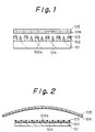
- a display as shown in Fig. 1 is known.
- a silicon dioxide (SiO 2 ) film 102 having cavities 102a is formed on a conductive flat silicon (Si) substrate 101.
- Gate electrodes 103 made of molybdenum (Mo), niobium (Nb), or the like are formed on the SiO 2 film 102 in the peripheral portions of the cavities 102a.
- a cathode 104 made of Mo or the like is formed on the Si substrate 101 in the cavity 102a.
- a fluorescent screen in which a fluorescent material 106 is formed on the flat glass plate 105 is arranged so as to face in parallel with the Si substrate 101 on which the cathode array is formed. The space between the fluorescent screen and the Si substrate 101 is sealed in a state in which it is held in vacuum.
- the above conventional flat panel display has a structure in which a differential pressure between the atmospheric pressure and the vacuum is held by only the glass plate 105 on which the fluorescent material 106 is formed. It is, accordingly, difficult to simply enlarge the screen from a viewpoint of the strength of the glass plate 105.
- Document EP-0,404,022 discloses the use of a plurality of cathodes formed on a substrate within a flat configuration image display apparatus.
- Vmin denotes a minimum voltage (absolute value) at which a current emission can be performed and Vmax indicates a maximum voltage (absolute value) at which a current emission can be executed without causing a discharge.
- Vmax indicates a maximum voltage (absolute value) at which a current emission can be executed without causing a discharge.
- the screen is formed by the glass plate of the convex curved shape, a large screen of the flat panel display can be realized. Moreover, since the space between the fluorescent screen and the screen and the space between the fluorescent screen and the substrate are vacuum, a differential pressure does not substantially exist on both sides of the fluorescent screen. Thus, even when the area of the fluorescent screen is increased in order to realize a large screen, no problem occurs with respect to the strength.
- the field evaporation sequentially occurs from the cathode whose radius of curvature of the tips is small. After the elapse of a predetermined time, the radii of curvatures of the tips of all of the cathodes constructing the cathode array are equalized. Due to this, the radii of curvatures of the tips of all of the cathodes constructing the cathode array can be easily aligned at a high precision. The field emission from each cathode can be uniformed.
- Fig. 4 is a cross sectional view showing a flat panel display according to the invention.
- an insulating film 202 such as an SiO 2 film having cavities 202a is formed on, for instance, a conductive flat Si substrate 201.
- a gate electrode 203 made of, for example, Mo or Nb is formed on the insulating film 202 in the peripheral portion of the cavity 202a.
- a cathode 204 made of a microtip is formed on the Si substrate 201 in the cavity 202a.
- the cathode array is formed by a number of cathodes 204.
- the insulating film 202 such as an SiO 2 film is first formed onto the Si substrate 201 by, for instance, a thermal oxidation method, a CVD method, or a sputtering method.
- a metal film made of, for example, Mo, Nb, or the like to form gate electrodes is formed onto the insulating film 202, by, e.g., a sputtering method or an electron beam evaporation depositing method.
- a resist pattern (not shown) having a shape corresponding to the gate electrodes to be formed is formed onto the metal film by a lithography.
- the gate electrodes 203 are formed.
- the insulating film 202 is etched by a wet etching method or a dry etching method by using the resist pattern and the gate electrodes 203 as masks, thereby forming the cavities 202a.
- an oblique evaporation deposition is performed onto the substrate surface from the direction which is inclined by a predetermined angle for the substrate surface by an electrode beam evaporation depositing method, thereby forming a peeling-off layer made of, for example, Al or Ni onto the gate electrodes.
- Mo as a material to form the cathodes is evaporation deposited onto the substrate surface from the direction perpendicular thereto by an electron beam evaporation depositing method.
- the cathodes 204 thus, are formed on the Si substrate 201 in the cavities 202a.
- the peeling-off layer is subsequently removed together with the metal film formed thereon by a lift-off method.
- the fluorescent screen in which the fluorescent material 206 is formed on the glass plate 205 is arranged so as to face the Si substrate 201 on which the cathode array is formed. Further, the spherical glass plate 207 serving as a screen is arranged on the outside of the fluorescent screen. The space between the fluorescent screen and the glass plate 207 is sealed in a state in which it is held in vacuum, thereby completing a desired flat panel display.
- the flat panel display can be formed as a large screen. Moreover, since both of the spaces on both sides of the fluorescent screen are vacuum, there is hardly a differential pressure between both sides of the fluorescent screen, so that a situation such that a force is applied to the fluorescent screen due to the differential pressure actually does not occur. Thus, even when an area of the fluorescent screen is enlarged to realize a large screen of the flat panel display, no problem occurs with respect to the strength.
- the screen is formed by the spherical glass plate 207.
- the screen is not always necessary to be formed in a spherical shape.
- it can be also formed in a cylindrical or other convex curved shape.
- the radii of curvatures of the tips of all of the cathodes constructing the cathode array can be easily made equal at a high accuracy.
- the luminances of the flat panel display can be uniformed.
Landscapes
- Engineering & Computer Science (AREA)
- Manufacturing & Machinery (AREA)
- Chemical & Material Sciences (AREA)
- Nanotechnology (AREA)
- Physics & Mathematics (AREA)
- Mathematical Physics (AREA)
- Theoretical Computer Science (AREA)
- Crystallography & Structural Chemistry (AREA)
- Cathode-Ray Tubes And Fluorescent Screens For Display (AREA)
- Cold Cathode And The Manufacture (AREA)
Claims (3)
- Flache Anzeigeeinrichtung für kalte Feldemission, mit einer Kathodenanordnung auf einem flachen Substrat, wobei die Kathode Tausende einzelner kegelförmiger Kathodenspitzen in der Größenordnung von µm auf dem Substrat umfasst, wobei die Spitzen durch Öffnungen in einer Isolierschicht auf dem Substrat vorstehen, wobei eine Gateelektrode auf einer Fläche der Isolierschicht ausgebildet ist und ein Fluoreszenzschirm mit einer Schicht aus fluoreszierendem Material auf einer Glasplatte so angeordnet ist, dass er der Kathodenanordnung so gegenübersteht, dass die Fluoreszenzschicht der Kathodenanordnung zugewandt ist, mit:einem Schirm aus einer kugelförmigen Glasplatte, der aus einer konvexen Glasplatte mit kugelförmigen Innen- und Außenflächen besteht, wobei der Fluoreszenzschirm zwischen dem Schirm aus der kugelförmigen Glasplatte und der Kathodenanordnung positioniert ist;wobei der Fluoreszenzschirm flach ist undwobei sich der Zwischenraum zwischen dem flachen Fluoreszenzschirm und dem Schirm aus der kugelförmigen Glasplatte sowie der Zwischenraum zwischen dem Fluoreszenzschirm und dem Substrat unter Vakuum befinden.
- Vorrichtung nach Anspruch 1, bei der das Vakuum zwischen dem flachen Fluoreszenzschirm und der kugelförmigen Glasplatte dasselbe wie das Vakuum im Zwischenraum zwischen dem Fluoreszenzschirm und dem Substrat ist.
- Vorrichtung nach Anspruch 1, bei der das Vakuum im Zwischenraum zwischen dem flachen Fluoreszenzschirm und der kugelförmigen Glasplatte verschieden vom Vakuum im Zwischenraum zwischen dem flachen Fluoreszenzschirm und dem Substrat ist.
Priority Applications (2)
| Application Number | Priority Date | Filing Date | Title |
|---|---|---|---|
| EP96107447A EP0729171B1 (de) | 1990-12-28 | 1991-12-19 | Verfahren zur Herstellung einer flachen Anzeigevorrichtung |
| EP96101002A EP0714114A1 (de) | 1990-12-28 | 1991-12-19 | Verfahren zur Herstellung einer flachen Anzeigevorrichtung |
Applications Claiming Priority (4)
| Application Number | Priority Date | Filing Date | Title |
|---|---|---|---|
| JP417501/90 | 1990-12-28 | ||
| JP41750190A JP3094459B2 (ja) | 1990-12-28 | 1990-12-28 | 電界放出型カソードアレイの製造方法 |
| JP2417502A JP3060546B2 (ja) | 1990-12-28 | 1990-12-28 | フラットパネルディスプレイ |
| JP417502/90 | 1990-12-28 |
Related Child Applications (3)
| Application Number | Title | Priority Date | Filing Date |
|---|---|---|---|
| EP96101002.2 Division-Into | 1991-12-19 | ||
| EP96101002A Division EP0714114A1 (de) | 1990-12-28 | 1991-12-19 | Verfahren zur Herstellung einer flachen Anzeigevorrichtung |
| EP96107447A Division EP0729171B1 (de) | 1990-12-28 | 1991-12-19 | Verfahren zur Herstellung einer flachen Anzeigevorrichtung |
Publications (3)
| Publication Number | Publication Date |
|---|---|
| EP0494425A2 EP0494425A2 (de) | 1992-07-15 |
| EP0494425A3 EP0494425A3 (en) | 1992-10-14 |
| EP0494425B1 true EP0494425B1 (de) | 1999-02-24 |
Family
ID=26583064
Family Applications (3)
| Application Number | Title | Priority Date | Filing Date |
|---|---|---|---|
| EP91121877A Expired - Lifetime EP0494425B1 (de) | 1990-12-28 | 1991-12-19 | Flache Anzeigeeinrichtung |
| EP96101002A Withdrawn EP0714114A1 (de) | 1990-12-28 | 1991-12-19 | Verfahren zur Herstellung einer flachen Anzeigevorrichtung |
| EP96107447A Expired - Lifetime EP0729171B1 (de) | 1990-12-28 | 1991-12-19 | Verfahren zur Herstellung einer flachen Anzeigevorrichtung |
Family Applications After (2)
| Application Number | Title | Priority Date | Filing Date |
|---|---|---|---|
| EP96101002A Withdrawn EP0714114A1 (de) | 1990-12-28 | 1991-12-19 | Verfahren zur Herstellung einer flachen Anzeigevorrichtung |
| EP96107447A Expired - Lifetime EP0729171B1 (de) | 1990-12-28 | 1991-12-19 | Verfahren zur Herstellung einer flachen Anzeigevorrichtung |
Country Status (4)
| Country | Link |
|---|---|
| US (1) | US5210462A (de) |
| EP (3) | EP0494425B1 (de) |
| KR (1) | KR100297881B1 (de) |
| DE (2) | DE69130920T2 (de) |
Families Citing this family (24)
| Publication number | Priority date | Publication date | Assignee | Title |
|---|---|---|---|---|
| US5536193A (en) | 1991-11-07 | 1996-07-16 | Microelectronics And Computer Technology Corporation | Method of making wide band gap field emitter |
| US5449970A (en) | 1992-03-16 | 1995-09-12 | Microelectronics And Computer Technology Corporation | Diode structure flat panel display |
| US5659224A (en) | 1992-03-16 | 1997-08-19 | Microelectronics And Computer Technology Corporation | Cold cathode display device |
| US5543684A (en) | 1992-03-16 | 1996-08-06 | Microelectronics And Computer Technology Corporation | Flat panel display based on diamond thin films |
| US6127773A (en) | 1992-03-16 | 2000-10-03 | Si Diamond Technology, Inc. | Amorphic diamond film flat field emission cathode |
| US5675216A (en) | 1992-03-16 | 1997-10-07 | Microelectronics And Computer Technololgy Corp. | Amorphic diamond film flat field emission cathode |
| GB2268324A (en) * | 1992-06-30 | 1994-01-05 | Ibm | Colour field emission display. |
| US5631664A (en) * | 1992-09-18 | 1997-05-20 | Olympus Optical Co., Ltd. | Display system utilizing electron emission by polarization reversal of ferroelectric material |
| CN1134754A (zh) | 1993-11-04 | 1996-10-30 | 微电子及计算机技术公司 | 制作平板显示系统和元件的方法 |
| GB2285168B (en) * | 1993-12-22 | 1997-07-16 | Marconi Gec Ltd | Electron field emission devices |
| US5729086A (en) * | 1995-02-28 | 1998-03-17 | Institute For Advanced Engineering | Field emission display panel having a main space and an auxiliary space |
| US5630741A (en) * | 1995-05-08 | 1997-05-20 | Advanced Vision Technologies, Inc. | Fabrication process for a field emission display cell structure |
| US5644188A (en) * | 1995-05-08 | 1997-07-01 | Advanced Vision Technologies, Inc. | Field emission display cell structure |
| US5763998A (en) * | 1995-09-14 | 1998-06-09 | Chorus Corporation | Field emission display arrangement with improved vacuum control |
| US5697825A (en) * | 1995-09-29 | 1997-12-16 | Micron Display Technology, Inc. | Method for evacuating and sealing field emission displays |
| US5646479A (en) * | 1995-10-20 | 1997-07-08 | General Motors Corporation | Emissive display including field emitters on a transparent substrate |
| US5692942A (en) * | 1995-11-30 | 1997-12-02 | The Boc Group, Inc. | Display forming method |
| FR2750785B1 (fr) * | 1996-07-02 | 1998-11-06 | Pixtech Sa | Procede de regeneration de micropointes d'un ecran plat de visualisation |
| US6198214B1 (en) | 1997-06-23 | 2001-03-06 | Fed Corporation | Large area spacer-less field emissive display package |
| US6259422B1 (en) | 1997-08-06 | 2001-07-10 | Canon Kabushiki Kaisha | Method for producing image-forming apparatus |
| GB2389959B (en) * | 2002-06-19 | 2006-06-14 | Univ Dundee | Improved field emission device |
| JP4115410B2 (ja) | 2004-03-12 | 2008-07-09 | キヤノン株式会社 | 電子放出素子、電子源ならびに画像表示装置の製造方法および電子放出素子の駆動方法 |
| CN1728330A (zh) * | 2004-07-29 | 2006-02-01 | 清华大学 | 场发射发光照明光源 |
| JP2007027018A (ja) * | 2005-07-21 | 2007-02-01 | Hitachi Ltd | ディスプレイパネルの製造方法及びアノードパネル |
Family Cites Families (14)
| Publication number | Priority date | Publication date | Assignee | Title |
|---|---|---|---|---|
| US2760119A (en) * | 1952-01-15 | 1956-08-21 | Products And Licensing Corp | Mural television screen |
| US2817002A (en) * | 1954-02-02 | 1957-12-17 | Research Corp | Fabrication of metal articles |
| US3467878A (en) * | 1966-06-27 | 1969-09-16 | Gen Electric | Electron discharge device with arrangement for replenishing emissive material on a smooth cathode surface |
| US3562881A (en) * | 1969-02-27 | 1971-02-16 | Nasa | Field-ionization electrodes |
| US3665241A (en) * | 1970-07-13 | 1972-05-23 | Stanford Research Inst | Field ionizer and field emission cathode structures and methods of production |
| FR2098954A5 (de) * | 1970-07-31 | 1972-03-10 | Anvar | |
| JPS58209844A (ja) * | 1982-05-31 | 1983-12-06 | Fujitsu Ltd | 電界電離型イオン源 |
| JPS60119053A (ja) * | 1983-11-30 | 1985-06-26 | Fujitsu Ltd | 高輝度イオンビ−ムの形成方法 |
| FR2568394B1 (fr) * | 1984-07-27 | 1988-02-12 | Commissariat Energie Atomique | Dispositif de visualisation par cathodoluminescence excitee par emission de champ |
| US4818914A (en) * | 1987-07-17 | 1989-04-04 | Sri International | High efficiency lamp |
| JPH01102834A (ja) * | 1987-10-15 | 1989-04-20 | Toshiba Corp | ガス放電型表示装置 |
| GB2227362B (en) * | 1989-01-18 | 1992-11-04 | Gen Electric Co Plc | Electronic devices |
| US5160871A (en) * | 1989-06-19 | 1992-11-03 | Matsushita Electric Industrial Co., Ltd. | Flat configuration image display apparatus and manufacturing method thereof |
| US5063323A (en) * | 1990-07-16 | 1991-11-05 | Hughes Aircraft Company | Field emitter structure providing passageways for venting of outgassed materials from active electronic area |
-
1991
- 1991-12-19 EP EP91121877A patent/EP0494425B1/de not_active Expired - Lifetime
- 1991-12-19 DE DE69130920T patent/DE69130920T2/de not_active Expired - Fee Related
- 1991-12-19 EP EP96101002A patent/EP0714114A1/de not_active Withdrawn
- 1991-12-19 DE DE69132385T patent/DE69132385T2/de not_active Expired - Fee Related
- 1991-12-19 EP EP96107447A patent/EP0729171B1/de not_active Expired - Lifetime
- 1991-12-23 KR KR1019910023846A patent/KR100297881B1/ko not_active Expired - Fee Related
- 1991-12-30 US US07/815,061 patent/US5210462A/en not_active Expired - Fee Related
Also Published As
| Publication number | Publication date |
|---|---|
| EP0494425A2 (de) | 1992-07-15 |
| EP0729171B1 (de) | 2000-08-23 |
| DE69132385T2 (de) | 2001-03-08 |
| DE69130920D1 (de) | 1999-04-01 |
| DE69130920T2 (de) | 1999-09-16 |
| US5210462A (en) | 1993-05-11 |
| EP0494425A3 (en) | 1992-10-14 |
| DE69132385D1 (de) | 2000-09-28 |
| EP0729171A2 (de) | 1996-08-28 |
| EP0729171A3 (de) | 1997-02-12 |
| KR100297881B1 (ko) | 2001-10-24 |
| EP0714114A1 (de) | 1996-05-29 |
| KR920013581A (ko) | 1992-07-29 |
Similar Documents
| Publication | Publication Date | Title |
|---|---|---|
| US5209687A (en) | Flat panel display apparatus and a method of manufacturing thereof | |
| US5210462A (en) | Flat panel display apparatus and a method of manufacturing thereof | |
| EP0483814B1 (de) | Feldemissionseinrichtung und Herstellungsverfahren | |
| US5587588A (en) | Multiple micro-tips field emission device | |
| US6522053B1 (en) | Field emission element, fabrication method thereof, and field emission display | |
| US5578900A (en) | Built in ion pump for field emission display | |
| US5729087A (en) | Inversion-type fed structure having auxiliary metal electrodes | |
| US5614795A (en) | Field emission device | |
| US5676578A (en) | Soft luminescence of field emission display | |
| KR20010041434A (ko) | 라지 에리어 전계 방출 소자 장치 및 그 제조 방법 | |
| US5378182A (en) | Self-aligned process for gated field emitters | |
| KR100314830B1 (ko) | 전계방출표시장치의제조방법 | |
| JP3094459B2 (ja) | 電界放出型カソードアレイの製造方法 | |
| US6036565A (en) | Method of fabricating a field emmision cold cathode | |
| JP3246137B2 (ja) | 電界放出カソード及び電界放出カソードの製造方法 | |
| US5631519A (en) | Field emission micro-tip | |
| KR100351068B1 (ko) | 전계방출표시장치및그제조방법 | |
| US7112920B2 (en) | Field emission source with plural emitters in an opening | |
| JP3060546B2 (ja) | フラットパネルディスプレイ | |
| US6426233B1 (en) | Uniform emitter array for display devices, etch mask for the same, and methods for making the same | |
| US20030042840A1 (en) | Gate-to-electrode connection in a flat panel display | |
| KR100238708B1 (ko) | 플래트패널디스플레이의 제조방법 | |
| JP3221425B2 (ja) | 微小開口の形成方法及び電界放出型冷陰極の製造方法 | |
| KR100274793B1 (ko) | 선형 전계방출 이미터 및 그의 제조방법 | |
| KR100343212B1 (ko) | 수평전계효과전자방출소자및그제조방법 |
Legal Events
| Date | Code | Title | Description |
|---|---|---|---|
| PUAI | Public reference made under article 153(3) epc to a published international application that has entered the european phase |
Free format text: ORIGINAL CODE: 0009012 |
|
| AK | Designated contracting states |
Kind code of ref document: A2 Designated state(s): DE FR GB |
|
| PUAL | Search report despatched |
Free format text: ORIGINAL CODE: 0009013 |
|
| AK | Designated contracting states |
Kind code of ref document: A3 Designated state(s): DE FR GB |
|
| 17P | Request for examination filed |
Effective date: 19930315 |
|
| 17Q | First examination report despatched |
Effective date: 19950725 |
|
| GRAG | Despatch of communication of intention to grant |
Free format text: ORIGINAL CODE: EPIDOS AGRA |
|
| GRAG | Despatch of communication of intention to grant |
Free format text: ORIGINAL CODE: EPIDOS AGRA |
|
| GRAH | Despatch of communication of intention to grant a patent |
Free format text: ORIGINAL CODE: EPIDOS IGRA |
|
| GRAH | Despatch of communication of intention to grant a patent |
Free format text: ORIGINAL CODE: EPIDOS IGRA |
|
| GRAA | (expected) grant |
Free format text: ORIGINAL CODE: 0009210 |
|
| AK | Designated contracting states |
Kind code of ref document: B1 Designated state(s): DE FR GB |
|
| XX | Miscellaneous (additional remarks) |
Free format text: TEILANMELDUNG 96101002.2 EINGEREICHT AM 24/01/96. |
|
| REF | Corresponds to: |
Ref document number: 69130920 Country of ref document: DE Date of ref document: 19990401 |
|
| ET | Fr: translation filed | ||
| PLBE | No opposition filed within time limit |
Free format text: ORIGINAL CODE: 0009261 |
|
| STAA | Information on the status of an ep patent application or granted ep patent |
Free format text: STATUS: NO OPPOSITION FILED WITHIN TIME LIMIT |
|
| 26N | No opposition filed | ||
| REG | Reference to a national code |
Ref country code: GB Ref legal event code: IF02 |
|
| PGFP | Annual fee paid to national office [announced via postgrant information from national office to epo] |
Ref country code: GB Payment date: 20021218 Year of fee payment: 12 |
|
| PGFP | Annual fee paid to national office [announced via postgrant information from national office to epo] |
Ref country code: DE Payment date: 20021219 Year of fee payment: 12 |
|
| PGFP | Annual fee paid to national office [announced via postgrant information from national office to epo] |
Ref country code: FR Payment date: 20031210 Year of fee payment: 13 |
|
| PG25 | Lapsed in a contracting state [announced via postgrant information from national office to epo] |
Ref country code: GB Free format text: LAPSE BECAUSE OF NON-PAYMENT OF DUE FEES Effective date: 20031219 |
|
| PG25 | Lapsed in a contracting state [announced via postgrant information from national office to epo] |
Ref country code: DE Free format text: LAPSE BECAUSE OF NON-PAYMENT OF DUE FEES Effective date: 20040701 |
|
| GBPC | Gb: european patent ceased through non-payment of renewal fee |
Effective date: 20031219 |
|
| PG25 | Lapsed in a contracting state [announced via postgrant information from national office to epo] |
Ref country code: FR Free format text: LAPSE BECAUSE OF NON-PAYMENT OF DUE FEES Effective date: 20050831 |
|
| REG | Reference to a national code |
Ref country code: FR Ref legal event code: ST |