EP0493014A1 - Antenne microbande - Google Patents
Antenne microbande Download PDFInfo
- Publication number
- EP0493014A1 EP0493014A1 EP91311860A EP91311860A EP0493014A1 EP 0493014 A1 EP0493014 A1 EP 0493014A1 EP 91311860 A EP91311860 A EP 91311860A EP 91311860 A EP91311860 A EP 91311860A EP 0493014 A1 EP0493014 A1 EP 0493014A1
- Authority
- EP
- European Patent Office
- Prior art keywords
- patch
- feed
- antenna
- short
- sections
- Prior art date
- Legal status (The legal status is an assumption and is not a legal conclusion. Google has not performed a legal analysis and makes no representation as to the accuracy of the status listed.)
- Withdrawn
Links
Images


Classifications
-
- H—ELECTRICITY
- H01—ELECTRIC ELEMENTS
- H01Q—ANTENNAS, i.e. RADIO AERIALS
- H01Q21/00—Antenna arrays or systems
- H01Q21/06—Arrays of individually energised antenna units similarly polarised and spaced apart
- H01Q21/061—Two dimensional planar arrays
- H01Q21/065—Patch antenna array
-
- H—ELECTRICITY
- H01—ELECTRIC ELEMENTS
- H01Q—ANTENNAS, i.e. RADIO AERIALS
- H01Q9/00—Electrically-short antennas having dimensions not more than twice the operating wavelength and consisting of conductive active radiating elements
- H01Q9/04—Resonant antennas
- H01Q9/0407—Substantially flat resonant element parallel to ground plane, e.g. patch antenna
Definitions
- This invention relates to patch antennas.
- the conventional half-wavelength rectangular patch antenna having a single feed point, may be regarded as a lossy resonant cavity, which loses, i.e. radiates, energy mainly from the two edges of the patch which are separated by the nominal half-wavelength resonant dimension.
- the two radiating edges may be viewed as a two-element, in-phase, slot array yielding a radiation pattern which peaks at broadside in a direction normal to the plane of the patch and tapers to a level typically 10dB below the peak at 90° from the normal, the actual level being dependent upon the permittivity of the substrate carrying the patch.
- the two edges Being a resonant structure, the two edges always radiate the applied signal with equal powers and with phase coherence.
- the radiation pattern of the antenna always has a peak centred on a boresight which is normal to the plane of the patch, i.e. the antenna's beam axis is aligned with that boresight.
- Many antenna applications demand a radiation pattern which is such that the beam axis is not centred on the normal boresight. It may even be that a null on the boresight is desired.
- Using conventional patch designs such radiation patterns can be achieved only by means of a phased array of patches and not by a single patch element.
- a patch antenna comprising two co-planar adjacent conductive patch sections, an underlying ground plane, adjacent edges of the patch sections being short-circuited to the ground plane, and feed means for feeding each patch section at a respective point remote from the adjacent edges, the beam axis of the antenna having a direction, in a plane normal to the short-circuited edges, which is dependent upon the relative phases of the signals at the feed points.
- this single conductive patch preferably has a resonant dimension normal to the common short-circuit and corresponding substantially to a half-wavelength at the operative frequency of the antenna.
- the feed means comprising respective feed striplines electrically coupled to the patch sections at the two feed points.
- the feed striplines may form continuous conductive layers with the patch sections at the feed points, there being a notch in each patch section in the vicinity of its feed stripline to provide impedance matching between the feed stripline and the patch section.
- the feed means may further comprise a common feed line to which the feed striplines are connected at a junction, the lengths of the two feed striplines determining the relative phases of the signals at the feed points.
- the feed striplines may present unequal impedance to the common feed line at the junction so that the signals have different magnitude at the feed points.
- the single conductive patch and the ground plane are preferably separated by an intervening dielectric substrate, the common short-circuit comprising a row of plated-through holes formed in the substrate.
- an antenna comprises a planar array of patch antennas, each as aforesaid, the patch antennas being arranged so that their short-circuited edges lie substantially parallel to one another and the common feed lines being coupled to a single feed line for the antenna, the relative signal phases and amplitudes at adjacent patch sections in the array determining the overall radiation pattern of the antenna.
- the antenna comprises the basic structure of a conductive patch 7, a ground plane layer 12 and an intervening dielectric substrate 11.
- the patch 7 is shown in the plan view of Figure 1 only the patch 7 is shown.
- the underlying ground plane 12 has a greater extent than the patch 7 in the normal manner.
- the antenna is suitably made of microstripline circuit board.
- the resonant length L o of the patch 7 corresponds nominally to a half-wavelength at the operative frequency of the antenna.
- Characteristic of the antenna is the provision of a short-circuit formed between the patch 7 and the ground plane layer 12 by means of a row of plated-through holes 10. As can be seen from Figure 1, the short-circuit formed by this row of holes 10 (and represented by the dotted line 17) extends parallel to and equi-distant from the two radiating edges 13,14 of the patch.
- the two patch sections 15,16 are fed at points remote from the short-circuit 17 by means of respective striplines 8, 9 ( Figure 1) each of which forms a continuous conductive layer at the feed point.
- the radiating edges 13,14 of the patch include respective notches 18,19 in the vicinity of the feed striplines 8,9.
- the notches 18,19 provide impedance matching between the patch sections and the feed striplines.
- the depth of each notch i.e. its extent in a direction normal to the radiating edge of the patch section, would normally be such that it presents an impedance equal to that of the feed stripline.
- a further factor in determining the notch depth is the width W of the patch.
- the width W determines the admittance of the radiating edges 13,14, which in turn, governs the variation in impedance along the patch length L o .
- the width of the notch should be sufficient to minimise coupling between the patch section and the feed stripline. A gap, on either side of the feed stripline, equivalent to the thickness of the substrate 11 has been found to be sufficient.
- the radiation pattern of the antenna is such that the beam axis lies in a plane normal to the short-circuit 17 and to the antenna.
- the beam axis is not essentially aligned with a boresight in this plane and normal to the antenna.
- the angle between the beam axis and the boresight is determined by the relative phases and amplitudes of the signals applied to the two patch sections 15,16 by means of the feed striplines 8,9.
- FIG. 3 shows, by way of example only, three different feed arrangements for the antenna which produce different angles between the beam axis and the normal boresight.
- the two striplines 8,9 are connected together at a T-junction 20 to a common feed line 21.
- the common feed line 21 will have an impedance of 50 ohms.
- the two patch sections 15,16 will be fed with signals of equal amplitude, but with a relative phase dependent on any difference in the lengths of the two striplines 8,9.
- the striplines 8,9 have equal lengths so that the two patch sections are fed with signals of the same phase.
- the edges 13,14 radiate in anti-phase to produce a null in the radiation pattern on the boresight.
- the T-junction 20 is 'offset' by a quarter-wavelength ( ⁇ o /4) in the substrate from the central position shown in Figure 3(a), the effect being that there is a difference in the length of the striplines 8,9 which corresponds to a half-wavelength in the substrate at the operative frequency.
- the patch sections are thus fed with signals which differ in phase by 180°, resulting in a radiation pattern having a peak centred on the boresight.
- the beam axis is aligned with the boresight using this feed arrangement.
- Figure 3(c) represents an intermediate position between the extremes of Figures 3(a) and 3(b), in which the offset X of the common feed line 21 at the T-junction 20 is less than a quarter-wavelength.
- This arrangement produces a 'squinted' radiation pattern in which the angle between the beam axis and the boresight is a function of the degree of the offset X and thus of the signal phase difference at the feed points of the two patch sections.
- the size of the patch 7 and the permittivity of the substrate 11 will also affect the angle off boresight which can be achieved. It will be appreciated, therefore, that, by varying the relative phase of the signals at the two feed points of the patch, the beam can be steered in a plane normal to the short-circuit and to the plane of the antenna.
- the short-circuit 17 is not essentially realised by means of plated-through holes, although this is a convenient and preferred method when the antenna is fabricated in microstripline.
- Alternatives include the use of a row of conducting pins inserted through the substrate or a plated physical slot in the board.
- the patch sections may be fed in a number of ways other than that described; for instance, by means of a coaxial cable having its centre conductor fed through the board and connected to the patch. Alternatively, there may be provided a capacitive coupling between a feed stripline and the patch. However, the use of a stripline conductor formed as an extension of the conductive patch layer is preferred from a fabrication viewpoint since the patch, feed line and ground plane can then all be formed on a single piece of microstripline circuit board.
- a patch antenna in accordance with the invention does not essentially comprise a single patch element divided into two patch sections by a common short-circuit.
- the two patch sections may be separate elements provided each section has a short-circuited edge to the common ground plane, and that the two short-circuited edges are disposed adjacent one another.
- such an arrangement is distinguished from that which occurs in a known array of quarter-wavelength patch elements in that in the known array the short-circuited edges of adjacent patches are not disposed adjacent one another, but rather with open-circuit edges facing short-circuit edges, i.e. in a repeated pattern of identically disposed patches. Even if the quarter-wavelength patches were arranged alternately, with (relatively) adjacent short-circuited edges, the radiating edges are not then known to be spaced apart by a resonant spacing.
- a patch antenna in accordance with the invention may be incorporated in a planar array, in which the elements in the array are fed in such manner that the overall beam shape and beam axis angle relative to boresight can be accurately controlled.
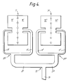
- Two adjacent elements in one possible array configuration are shown, by way of example only, in Figure 4, to which reference is now made. Although only two patches 7′, 7 ⁇ are shown, the array would, of course, normally comprise a greater number of elements.
- each patch is fed with signals which are in anti-phase, hence the unequal lengths of the pairs of striplines 8′, 9′ and 8 ⁇ , 9 ⁇ on either side of their respective T-junctions 20′ and 20 ⁇ .
- the signals at the two feed points of each patch have unequal magnitudes by virtue of the two striplines in each pair having different widths and therefore different impedances.
- the striplines 8′ and 9 ⁇ which feed the 'outer' patch sections 15′ and 16 ⁇ have a lesser width (i.e. higher impedance) than the striplines 9′ and 8 ⁇ which feed the 'inner' patch sections 16′ and 15 ⁇ .
- This arrangement gives rise to an overall radiation characteristic having a narrower central beam and reduced sidelobe levels than can be achieved using arrays of conventional patch elements. Further adjustment of the phase and amplitude conditions at the feed points of the patches may be used to 'fine tune' the beam shape according to requirements.
- the feed lines 21′,21 ⁇ for the two patches are coupled to a main feed line 23 for the antenna by means of a T-junction 22.
- the additional patches in a larger array would be similarly coupled to the main feed line in a conventional 'tree' structure.
Landscapes
- Variable-Direction Aerials And Aerial Arrays (AREA)
- Waveguide Aerials (AREA)
Applications Claiming Priority (2)
| Application Number | Priority Date | Filing Date | Title |
|---|---|---|---|
| GB9027776 | 1990-12-21 | ||
| GB909027776A GB9027776D0 (en) | 1990-12-21 | 1990-12-21 | Patch antenna |
Publications (1)
| Publication Number | Publication Date |
|---|---|
| EP0493014A1 true EP0493014A1 (fr) | 1992-07-01 |
Family
ID=10687423
Family Applications (1)
| Application Number | Title | Priority Date | Filing Date |
|---|---|---|---|
| EP91311860A Withdrawn EP0493014A1 (fr) | 1990-12-21 | 1991-12-20 | Antenne microbande |
Country Status (3)
| Country | Link |
|---|---|
| EP (1) | EP0493014A1 (fr) |
| JP (1) | JPH0548322A (fr) |
| GB (2) | GB9027776D0 (fr) |
Cited By (6)
| Publication number | Priority date | Publication date | Assignee | Title |
|---|---|---|---|---|
| FR2772517A1 (fr) * | 1997-12-11 | 1999-06-18 | Alsthom Cge Alcatel | Antenne multifrequence realisee selon la technique des microrubans et dispositif incluant cette antenne |
| WO2008127701A1 (fr) * | 2007-04-11 | 2008-10-23 | Vubiq, Incorporated | Antenne en onde entière à di-plaque |
| CN104051855A (zh) * | 2013-03-15 | 2014-09-17 | 香港城市大学 | 贴片天线 |
| WO2015181510A1 (fr) * | 2014-05-28 | 2015-12-03 | Kabushiki Kaisha Toshiba | Antenne |
| WO2016012738A1 (fr) * | 2014-07-22 | 2016-01-28 | Kabushiki Kaisha Toshiba | Antenne et procédé de fabrication d'une antenne |
| WO2018171227A1 (fr) * | 2017-03-18 | 2018-09-27 | 深圳市景程信息科技有限公司 | Antenne à structure en pont |
Families Citing this family (8)
| Publication number | Priority date | Publication date | Assignee | Title |
|---|---|---|---|---|
| GB2277640A (en) * | 1993-04-07 | 1994-11-02 | Woldroy Limited | Antenna |
| DE19614362C1 (de) * | 1996-04-11 | 1997-07-31 | Siemens Ag | Antenne für ein Diebstahlschutzsystem eines Kraftfahrzeugs |
| JP2000332523A (ja) * | 1999-05-24 | 2000-11-30 | Hitachi Ltd | 無線タグ、その製造方法及びその配置方法 |
| GB2358533A (en) * | 2000-01-21 | 2001-07-25 | Dynex Semiconductor Ltd | Antenna; feed; alarm sensor |
| GB2369497B (en) * | 2000-11-28 | 2004-03-24 | Harada Ind | Multiband vehicular telephone antenna |
| JP5408501B2 (ja) | 2010-08-31 | 2014-02-05 | 株式会社吉野工業所 | 合成樹脂製壜体 |
| WO2017064856A1 (fr) * | 2015-10-14 | 2017-04-20 | 日本電気株式会社 | Antenne de réseau à plaque, son procédé de commande de directivité et dispositif sans fil utilisant une antenne de réseau à plaque |
| TWI752780B (zh) * | 2020-12-31 | 2022-01-11 | 啓碁科技股份有限公司 | 寬波束之天線結構 |
Citations (3)
| Publication number | Priority date | Publication date | Assignee | Title |
|---|---|---|---|---|
| US4040060A (en) * | 1976-11-10 | 1977-08-02 | The United States Of America As Represented By The Secretary Of The Navy | Notch fed magnetic microstrip dipole antenna with shorting pins |
| JPS63222503A (ja) * | 1987-03-12 | 1988-09-16 | Sumitomo Electric Ind Ltd | アンテナ |
| EP0345454A1 (fr) * | 1988-05-13 | 1989-12-13 | Yagi Antenna Co., Ltd. | Antenne réseau à microruban |
Family Cites Families (4)
| Publication number | Priority date | Publication date | Assignee | Title |
|---|---|---|---|---|
| US4320401A (en) * | 1978-05-16 | 1982-03-16 | Ball Corporation | Broadband microstrip antenna with automatically progressively shortened resonant dimensions with respect to increasing frequency of operation |
| US4367474A (en) * | 1980-08-05 | 1983-01-04 | The United States Of America As Represented By The Secretary Of The Army | Frequency-agile, polarization diverse microstrip antennas and frequency scanned arrays |
| US4379296A (en) * | 1980-10-20 | 1983-04-05 | The United States Of America As Represented By The Secretary Of The Army | Selectable-mode microstrip antenna and selectable-mode microstrip antenna arrays |
| JPS6171702A (ja) * | 1984-09-17 | 1986-04-12 | Matsushita Electric Ind Co Ltd | 小形アンテナ |
-
1990
- 1990-12-21 GB GB909027776A patent/GB9027776D0/en active Pending
-
1991
- 1991-12-20 GB GB9127149A patent/GB2252676A/en not_active Withdrawn
- 1991-12-20 JP JP35530991A patent/JPH0548322A/ja active Pending
- 1991-12-20 EP EP91311860A patent/EP0493014A1/fr not_active Withdrawn
Patent Citations (3)
| Publication number | Priority date | Publication date | Assignee | Title |
|---|---|---|---|---|
| US4040060A (en) * | 1976-11-10 | 1977-08-02 | The United States Of America As Represented By The Secretary Of The Navy | Notch fed magnetic microstrip dipole antenna with shorting pins |
| JPS63222503A (ja) * | 1987-03-12 | 1988-09-16 | Sumitomo Electric Ind Ltd | アンテナ |
| EP0345454A1 (fr) * | 1988-05-13 | 1989-12-13 | Yagi Antenna Co., Ltd. | Antenne réseau à microruban |
Non-Patent Citations (2)
| Title |
|---|
| IEEE AP-S INTERNATIONAL SYMPOSIUM DIGEST; ANTENNAS AND PROPAGATION vol. II, June 1989, NEW YORK, US pages 882 - 885; WANG, J. ET AL.: 'Design Study of a Low Sidelobe Microstrip Antenna Array and Feed Network.' * |
| PATENT ABSTRACTS OF JAPAN vol. 13, no. 16 (E-703)(3364) 13 January 1989 & JP-A-63 222 503 ( SUMITOMO ELECTRIC IND ) 16 September 1988 * |
Cited By (10)
| Publication number | Priority date | Publication date | Assignee | Title |
|---|---|---|---|---|
| FR2772517A1 (fr) * | 1997-12-11 | 1999-06-18 | Alsthom Cge Alcatel | Antenne multifrequence realisee selon la technique des microrubans et dispositif incluant cette antenne |
| EP0924797A1 (fr) * | 1997-12-11 | 1999-06-23 | Alcatel | Antenne multifréquence réalisée selon la technique des microrubans, et dispositif incluant cette antenne |
| US6133879A (en) * | 1997-12-11 | 2000-10-17 | Alcatel | Multifrequency microstrip antenna and a device including said antenna |
| WO2008127701A1 (fr) * | 2007-04-11 | 2008-10-23 | Vubiq, Incorporated | Antenne en onde entière à di-plaque |
| US7868841B2 (en) | 2007-04-11 | 2011-01-11 | Vubiq Incorporated | Full-wave di-patch antenna |
| CN104051855A (zh) * | 2013-03-15 | 2014-09-17 | 香港城市大学 | 贴片天线 |
| WO2015181510A1 (fr) * | 2014-05-28 | 2015-12-03 | Kabushiki Kaisha Toshiba | Antenne |
| WO2016012738A1 (fr) * | 2014-07-22 | 2016-01-28 | Kabushiki Kaisha Toshiba | Antenne et procédé de fabrication d'une antenne |
| WO2016012791A1 (fr) * | 2014-07-22 | 2016-01-28 | Toshiba Research Europe Limited | Antenne et procédé associé |
| WO2018171227A1 (fr) * | 2017-03-18 | 2018-09-27 | 深圳市景程信息科技有限公司 | Antenne à structure en pont |
Also Published As
| Publication number | Publication date |
|---|---|
| GB9127149D0 (en) | 1992-02-19 |
| GB2252676A (en) | 1992-08-12 |
| GB9027776D0 (en) | 1991-06-12 |
| JPH0548322A (ja) | 1993-02-26 |
Similar Documents
| Publication | Publication Date | Title |
|---|---|---|
| US4125838A (en) | Dual asymmetrically fed electric microstrip dipole antennas | |
| USRE29911E (en) | Microstrip antenna structures and arrays | |
| US5229777A (en) | Microstrap antenna | |
| US3971032A (en) | Dual frequency microstrip antenna structure | |
| US4069483A (en) | Coupled fed magnetic microstrip dipole antenna | |
| US4054874A (en) | Microstrip-dipole antenna elements and arrays thereof | |
| US4063246A (en) | Coplanar stripline antenna | |
| US4623894A (en) | Interleaved waveguide and dipole dual band array antenna | |
| EP0447218B1 (fr) | Antenne microbande pour plusieurs fréquences | |
| US4843400A (en) | Aperture coupled circular polarization antenna | |
| EP0456680B1 (fr) | Reseaux d'antennes | |
| US4414550A (en) | Low profile circular array antenna and microstrip elements therefor | |
| US4843403A (en) | Broadband notch antenna | |
| CA1237808A (fr) | Antenne dipole a elements incrustes croises | |
| US5675345A (en) | Compact antenna with folded substrate | |
| US4370657A (en) | Electrically end coupled parasitic microstrip antennas | |
| US4833482A (en) | Circularly polarized microstrip antenna array | |
| US3987455A (en) | Microstrip antenna | |
| EP0257881A2 (fr) | Antenne à fente constituée par un guide d'onde et réseau de celle-ci | |
| EP0493014A1 (fr) | Antenne microbande | |
| US6087988A (en) | In-line CP patch radiator | |
| US6014112A (en) | Simplified stacked dipole antenna | |
| US4918457A (en) | Antenna formed of strip transmission lines with non-conductive coupling | |
| US3978487A (en) | Coupled fed electric microstrip dipole antenna | |
| JP3045536B2 (ja) | 強制励振アレイアンテナ |
Legal Events
| Date | Code | Title | Description |
|---|---|---|---|
| PUAI | Public reference made under article 153(3) epc to a published international application that has entered the european phase |
Free format text: ORIGINAL CODE: 0009012 |
|
| AK | Designated contracting states |
Kind code of ref document: A1 Designated state(s): DE ES FR IT SE |
|
| STAA | Information on the status of an ep patent application or granted ep patent |
Free format text: STATUS: THE APPLICATION IS DEEMED TO BE WITHDRAWN |
|
| 18D | Application deemed to be withdrawn |
Effective date: 19930105 |