EP0492203B1 - Device for connecting and disconnecting an electrical connector - Google Patents
Device for connecting and disconnecting an electrical connector Download PDFInfo
- Publication number
- EP0492203B1 EP0492203B1 EP91120893A EP91120893A EP0492203B1 EP 0492203 B1 EP0492203 B1 EP 0492203B1 EP 91120893 A EP91120893 A EP 91120893A EP 91120893 A EP91120893 A EP 91120893A EP 0492203 B1 EP0492203 B1 EP 0492203B1
- Authority
- EP
- European Patent Office
- Prior art keywords
- catch
- movable
- inflexible
- housing
- bar
- Prior art date
- Legal status (The legal status is an assumption and is not a legal conclusion. Google has not performed a legal analysis and makes no representation as to the accuracy of the status listed.)
- Expired - Lifetime
Links
- 238000003780 insertion Methods 0.000 claims description 10
- 230000037431 insertion Effects 0.000 claims description 10
- 230000000284 resting effect Effects 0.000 claims 1
- 238000012856 packing Methods 0.000 description 2
- 239000004020 conductor Substances 0.000 description 1
- 230000005670 electromagnetic radiation Effects 0.000 description 1
Images


Classifications
-
- H—ELECTRICITY
- H01—ELECTRIC ELEMENTS
- H01R—ELECTRICALLY-CONDUCTIVE CONNECTIONS; STRUCTURAL ASSOCIATIONS OF A PLURALITY OF MUTUALLY-INSULATED ELECTRICAL CONNECTING ELEMENTS; COUPLING DEVICES; CURRENT COLLECTORS
- H01R13/00—Details of coupling devices of the kinds covered by groups H01R12/70 or H01R24/00 - H01R33/00
- H01R13/62—Means for facilitating engagement or disengagement of coupling parts or for holding them in engagement
- H01R13/629—Additional means for facilitating engagement or disengagement of coupling parts, e.g. aligning or guiding means, levers, gas pressure electrical locking indicators, manufacturing tolerances
-
- H—ELECTRICITY
- H05—ELECTRIC TECHNIQUES NOT OTHERWISE PROVIDED FOR
- H05K—PRINTED CIRCUITS; CASINGS OR CONSTRUCTIONAL DETAILS OF ELECTRIC APPARATUS; MANUFACTURE OF ASSEMBLAGES OF ELECTRICAL COMPONENTS
- H05K7/00—Constructional details common to different types of electric apparatus
- H05K7/14—Mounting supporting structure in casing or on frame or rack
- H05K7/1401—Mounting supporting structure in casing or on frame or rack comprising clamping or extracting means
- H05K7/1402—Mounting supporting structure in casing or on frame or rack comprising clamping or extracting means for securing or extracting printed circuit boards
- H05K7/1405—Mounting supporting structure in casing or on frame or rack comprising clamping or extracting means for securing or extracting printed circuit boards by clips or resilient members, e.g. hooks
Definitions
- the present invention concerns a device for connecting and disconnecting an electrical connector according to the preamble of claim 1.
- electrical connectors have to meet special requirements. They must be designed such that their contacts do not become disconnected when subjected to different loads and stresses, such as those imposed by vibration, temperature differences, etc. In addition they must be user friendly, i.e. the must be easy to connect and disconnect.
- connectors must comprise latch means for connection and disconnection. Such means ensure that contacts are reliably closed and prevented from automatically opening during operation.
- European patent application 0 369 025 describes a device by which cards can be connected to and disconnected from a board.
- This device comprises a resilient latch member which is connected to the card and has a movable end portion, and an operating lever which is pivotably arranged on the card.
- Operating lever and latch member are positioned relative to each other such that when the operating lever is actuated, its curved surface causes the latch member to perform a translatory movement, so that card and board are electrically connected.
- the movable end portion then drops into a groove provided on the operating lever where it remains so that the card is fixed in that position.
- This prior art device has the disadvantage that the insertion force is permanently exerted on the board, so that, while the card is connected, the board is subject to considerable stress. In addition, it cannot avoided that the great number of contacts to be made by the connector increases the insertion force such that it bends the board. A board permanently bent in that way develops cracks which damage the printed conductor circuits.
- Another disadvantage is that for the previously described reasons the connector is only suitable for a limited number of contacts, so that large cards with very many contacts cannot be latched by the prior art device. As a result, the functions involved have to be distributed over several cards, which in turn necessitates larger housings.
- the device constituting its subject matter allows linking connectors with a very large number of contacts.
- the surface areas of the connector components are subject to pressure only during connection. Once electrical connection has been made, the pressure exerted on the connector largely disappears.
- This permits increasing the functional density of cards used, for example, in data processing.
- the advantage of this is that the space required for card storage is reduced and that smaller size boards may be used.
- particular functions on the board are rendered superfluous, as fewer cards are required. This, in turn, simplifies in particular the production of the cards.
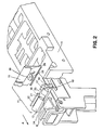
- Fig. 1 shows one or several cards 3 inserted in parallel in a housing 1 where they are connected to a board 5.
- the cards 3, in particular electronic cards, are generally accommodated in a protection housing 6 shielding them against electromagnetic radiation.
- Protection housing 6 has an aperture from which a contact connector part 4, linked with a contact connector part 7 of the board 5, protrudes.
- the top and the bottom corner on one side of the protection housing 6 are fitted with one latch 9 each which is pivotably supported on housing 6. If the protection housing 6 for shielding the card 3 is dispensed with for technical reasons, latch 9 may be fixed to the card 3 directly.
- Latch bars 11 may be arranged on housing 1 individually or jointly.
- Fig. 2 shows how the individual parts of the device according to the invention are associated.
- Catch bar 11 consists of an inflexible catch element 13 and a flexible catch element 15 which may be a U-shaped spring.
- the inflexible catch element 13 is fixed to housing 1.
- the flexible catch element 15 is designed as an independent element and arranged on the inflexible catch element 13.
- the inflexible catch element 13 has two legs 17, 18 extending orthogonally to each other, the inflexible catch element 13 being positioned on housing 1 such that one leg 18 is arranged parallel to housing 1 whereas the other leg 17 extends orthogonally to leg 18.
- the upper region of leg 17 is provided with a recess 19 so that two bars 21, 22, extending parallel to each other and the surface of leg 18, connected to housing 1, are formed on either side.
- the two bars 21, 22 are interrupted by a further recess 24, 25.
- the U-shaped spring 15 is fixed to the inflexible catch element 13 such that the two legs of spring 15 enclose bar 22 so that the bent portion of the spring 15 rests against the inside of bar 22.
- bar 22 acts as a stop.
- One leg 26 of the spring 15 is provided on its movable end with a tongue 28 projecting from spring 15 and which is positioned orthogonally to leg 26 of the spring 15.
- a cam 30 is arranged on this tongue 28, a cam 30 is arranged.
- Spring 15 is positoned on bar 22 such that the projecting tongue 28 is reciprocally movable parallel to the base of the recess 24 between bars 21, 22.
- Bar 21 is ramp-shaped so that latch 9 may be readily moved across bar 21.
- Cam 30 determines the point up to which latch 9 has to be moved for electrical connection. Having reached that point, latch 9 snaps into place behind cam 30.
- cam 30 is suspended from a spring 15, latch 9 along with the associated card 3 moves back in the direction of arrow A opposite that of the insertion force up to a point at which the pressure on the connector is almost zero. Disconnection of the connector is also prevented by the fact that the width of latch 9 enclosing cam 30 exceeds the size of the recess 24 in bar 21, so that the return movement of latch 9 with the card 3 is stopped on the inside of the bar 21.
- Fig. 3 shows the device according to the invention as card 3 and board 5 are being connected.
- Latches 9 are arranged in the upper and lower corners of the protection housing 6. If the protection housing is omitted for technical reasons, latches 9 may be arranged on the card 3 directly.
- Latches 9 are pivotably positioned on housing 6. They are pivotable about an axis C such that they are subdivided into two lever arms 35 and 36 of different length, which are arranged in S-shape relative to each other.
- the longer lever arm 36 of latch 9 is moved by hand or other means in the direction of arrow B.
- the short lever 35 of latch 9 engages a recess 37 on housing 1 as soon as the protection housing 6 with the card 3 arranged thereon is in engagement.
- a latch pawl 40 whose end is provided with a perpendicular latch nose 38, is arranged on the longer lever arm 36.
- the short lever arm 35 acts as a toggle lever, i.e. when the longer lever arm 36 with the latch pawl 40 for engaging cam 30 is moved in the direction of arrow D, the short lever arm 35 engages the recess 37 in housing 1, leading to an additional insertion force being exerted on the card and the protection housing 6. This additional force electrically connects the contact connector part 4 of the card to the contact connector part 7 of the board 5.
- latch pawl 40 engages cam 30 with its latch nose 38.
- the magnitude of the force required for connecting card 3 and board 5 is determined by the position of cam 30, i.e. the position of cam 30 determines the additional distance Y by which the card has to be moved before the latch nose 38 of the pawl 40 is capable of engaging cam 30.
- the insertion force must at least exceed the sum of the spring and frictional forces of the connector contacts. The load the insertion force exerts on the card 3 and the board 5 disappears immediately after the spring forces of the connector contacts have been overcome. To this end, the movable cam 30 is used which balances the pressure between card 3 and board 5.
- the insertion force required depends upon the number of contacts to be made when card 3 and board 5 are connected and the position of cam 30 on the inflexible catch element 13.
- the device according to the invention is adaptable to connectors with varying numbers of contacts.
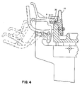
- Fig. 4 shows the device according to the invention in the unloaded state, i.e. after card 3 and board 5 have been electrically connnected.
- the movable cam 30 balances the pressure between card 3 and board 5. As a result of this and the change in the position of cam 30 in the direction of arrow A, the spring 15, supporting cam 30, is tensioned. Spring 15 is designed such that contacts are not inadvertently opened. For this purpose, the force required for further tensioning the spring 15 must exceed the sum of the frictional forces opening the contacts.
- Fig. 5 shows in particular the function of recesses 24, 25 on the inflexible catch element 13. Recess 24 allows cam 30 to move on the inflexible catch element 13 such that the pressure between card 3 and board 5 is balanced.
- the device according to the invention renders an inflexible catch element 13 superfluous, so that spring 15 and cam 30 may be fixed to housing 1, for example. It is also technically feasible for the inflexible catch element 13 to consist of a flat plate which is directly connected to housing 1. In this case, spring 15 would surround the plate such that it is self-supporting thereon.
- Fig. 6 shows in particular the design of the spring 15 and the inflexible catch element 13 for several cards 3 arranged in parallel.
- Spring 15 consists of one part 15a, its legs being separated from each other by a recess 42 so that one movable spring leg is associated with each card 3 or latch 9.
- Each spring leg is fitted with a tongue 28 and a cam 30 positioned thereon.
- the inflexible catch element also consists of one part 13a and has an elongated recess 19 forming two bars 21, 22, arranged parallel to each other, over the entire length of the inflexible catch part 13a.
- Each spring leg is also associated with a further recess 24, 25 which allows cam 30 to move for reducing the pressure between card 3 and board 5.
- Recess 24 is positioned such that the two bars 21, 22 are interrupted. The size of the interruption allows cam 30 to pass.
- the advantages of the device according to the present invention are that in particular for connector contacts connected by applying a predetermined force, the packing density of the card is almost insignificant.
- the present invention allows the connection of cards of maximum packing density without the board to which they are connected being damaged by the insertion force. Further advantages are that the device according to the invention is easy and inexpensive to produce.
Landscapes
- Engineering & Computer Science (AREA)
- Microelectronics & Electronic Packaging (AREA)
- Details Of Connecting Devices For Male And Female Coupling (AREA)
- Mounting Of Printed Circuit Boards And The Like (AREA)
- Coupling Device And Connection With Printed Circuit (AREA)
Applications Claiming Priority (2)
| Application Number | Priority Date | Filing Date | Title |
|---|---|---|---|
| DE4042060A DE4042060C1 (OSRAM) | 1990-12-28 | 1990-12-28 | |
| DE4042060 | 1990-12-28 |
Publications (2)
| Publication Number | Publication Date |
|---|---|
| EP0492203A1 EP0492203A1 (en) | 1992-07-01 |
| EP0492203B1 true EP0492203B1 (en) | 1995-08-09 |
Family
ID=6421600
Family Applications (1)
| Application Number | Title | Priority Date | Filing Date |
|---|---|---|---|
| EP91120893A Expired - Lifetime EP0492203B1 (en) | 1990-12-28 | 1991-12-05 | Device for connecting and disconnecting an electrical connector |
Country Status (4)
| Country | Link |
|---|---|
| US (1) | US5151041A (OSRAM) |
| EP (1) | EP0492203B1 (OSRAM) |
| JP (1) | JPH0817276B2 (OSRAM) |
| DE (2) | DE4042060C1 (OSRAM) |
Families Citing this family (12)
| Publication number | Priority date | Publication date | Assignee | Title |
|---|---|---|---|---|
| JPH01104389A (ja) * | 1987-10-17 | 1989-04-21 | Nippon Steel Corp | 鉄鋼排水処理方法 |
| DE19508605C1 (de) * | 1995-03-10 | 1996-07-11 | Harting Elektronik Gmbh | Elektrische Steckverbindung |
| DE19526330C2 (de) * | 1995-07-19 | 2000-09-21 | Ibm | Vorrichtung zur Herstellung einer elektrischen und/oder optischen Verbindung |
| DE19533569C2 (de) * | 1995-09-11 | 1997-08-07 | Ibm | Vorrichtung zur Herstellung einer Verbindung mit einer Leiterplatte |
| FR2743977B1 (fr) * | 1996-01-19 | 1998-02-06 | Gec Alsthom Transport Sa | Tiroir pour cartes electroniques a embrochement et debrochage automatiques et tiroir et son coffre |
| JP3442661B2 (ja) * | 1998-08-10 | 2003-09-02 | 矢崎総業株式会社 | レバー嵌合式コネクタ |
| US6802727B2 (en) * | 2001-12-06 | 2004-10-12 | International Business Machines Corporation | Apparatus for and method of connecting connectors |
| KR100505728B1 (ko) * | 2001-12-24 | 2005-08-03 | 주식회사 포스코 | 폐산 재생장치 및 이로부터 재생된 산을 이용한 알칼리폐수 처리방법 |
| US6884096B2 (en) * | 2003-04-29 | 2005-04-26 | International Business Machines Corporation | Apparatus for positioning an electrical assembly within a housing |
| DE102011001069B4 (de) * | 2011-03-03 | 2018-03-22 | Harting Electric Gmbh & Co. Kg | Verfahren zum Verriegeln eines ersten Systems von Steckverbindern mit einem zweiten System von Steckverbindern |
| CN105302234B (zh) * | 2014-07-16 | 2019-04-30 | 纬创资通股份有限公司 | 可用来拆装一扩展卡模块的固定机构及电子装置 |
| CZ307861B6 (cs) * | 2018-04-26 | 2019-07-03 | SQS Vláknová optika a.s. | Zasouvací a vysouvací zařízení pro spojování a rozpojování optických a/nebo elektrických konektorů |
Family Cites Families (8)
| Publication number | Priority date | Publication date | Assignee | Title |
|---|---|---|---|---|
| US2993187A (en) * | 1960-06-29 | 1961-07-18 | South Chester Corp | Module board fastener |
| US3476258A (en) * | 1967-05-18 | 1969-11-04 | Friden Inc | Board insertion and extraction system |
| CA1112348A (en) * | 1979-06-29 | 1981-11-10 | Ernest C. Leung | Latching lever for printed circuit boards |
| DE3171164D1 (en) * | 1980-01-30 | 1985-08-08 | Lucas Ind Plc | Closed loop control of i.c. engine idling speed |
| JPS57163793U (OSRAM) * | 1981-04-09 | 1982-10-15 | ||
| US4549334A (en) * | 1982-11-16 | 1985-10-29 | Lloyd Miller | Fabric mounting track system |
| US5140501A (en) * | 1988-04-30 | 1992-08-18 | Fujitsu Limited | Mechanism for inserting and withdrawing printed board unit of electronics circuit device |
| JPH0260290U (OSRAM) * | 1988-10-25 | 1990-05-02 |
-
1990
- 1990-12-28 DE DE4042060A patent/DE4042060C1/de not_active Expired - Lifetime
-
1991
- 1991-10-22 US US07/781,570 patent/US5151041A/en not_active Expired - Fee Related
- 1991-11-21 JP JP3355490A patent/JPH0817276B2/ja not_active Expired - Lifetime
- 1991-12-05 EP EP91120893A patent/EP0492203B1/en not_active Expired - Lifetime
- 1991-12-05 DE DE69112005T patent/DE69112005T2/de not_active Expired - Fee Related
Also Published As
| Publication number | Publication date |
|---|---|
| DE4042060C1 (OSRAM) | 1992-06-25 |
| JPH0645029A (ja) | 1994-02-18 |
| US5151041A (en) | 1992-09-29 |
| DE69112005T2 (de) | 1996-04-18 |
| EP0492203A1 (en) | 1992-07-01 |
| DE69112005D1 (de) | 1995-09-14 |
| JPH0817276B2 (ja) | 1996-02-21 |
Similar Documents
| Publication | Publication Date | Title |
|---|---|---|
| EP0492203B1 (en) | Device for connecting and disconnecting an electrical connector | |
| EP0929129B1 (en) | Card edge connector with a pair of latching devices | |
| US4071722A (en) | Latch and switch interlock safety structure | |
| US6149466A (en) | Compact smart card electrical connector | |
| US5342213A (en) | IC socket | |
| US4872845A (en) | Retention means for chip carrier sockets | |
| KR100256936B1 (ko) | 보강 래치를 갖춘 커넥터 | |
| US5885095A (en) | Electrical connector assembly with mounting hardware and protective cover | |
| US6576853B2 (en) | Switch exhibition non-unidirectional displacement | |
| US6551120B2 (en) | Card retention mechanism | |
| US6036520A (en) | Electrical connector for flat circuitry | |
| US5775950A (en) | Card-edge connector | |
| US6146171A (en) | Electrical connector for flat circuitry | |
| US5169345A (en) | Contact frame for an i.c. card reader | |
| US4257028A (en) | Remote socket for DIP components | |
| US5669782A (en) | Electrical connector | |
| US5154644A (en) | Edge connector for a printed circuit card | |
| US4006955A (en) | Card retainer | |
| US6186811B1 (en) | Electrical connector for flat circuitry | |
| KR100699210B1 (ko) | 장착 대상물에 고정되며 카드 커넥터에 삽입되는 카드와접촉하는 스토퍼를 갖는 카드 커넥터 | |
| US4594490A (en) | Terminal pin shorting switch apparatus | |
| EP0401585B1 (en) | Hooking device for connectors of printed wired artworks | |
| JP4370003B2 (ja) | 電気的接続もしくは光学的接続またはその両方の接続装置 | |
| JPH10511499A (ja) | カードエッジコネクター装置 | |
| WO1994029933A1 (en) | Electrical connector |
Legal Events
| Date | Code | Title | Description |
|---|---|---|---|
| PUAI | Public reference made under article 153(3) epc to a published international application that has entered the european phase |
Free format text: ORIGINAL CODE: 0009012 |
|
| AK | Designated contracting states |
Kind code of ref document: A1 Designated state(s): DE FR GB |
|
| 17P | Request for examination filed |
Effective date: 19921022 |
|
| 17Q | First examination report despatched |
Effective date: 19941114 |
|
| GRAA | (expected) grant |
Free format text: ORIGINAL CODE: 0009210 |
|
| AK | Designated contracting states |
Kind code of ref document: B1 Designated state(s): DE FR GB |
|
| REF | Corresponds to: |
Ref document number: 69112005 Country of ref document: DE Date of ref document: 19950914 |
|
| ET | Fr: translation filed | ||
| PGFP | Annual fee paid to national office [announced via postgrant information from national office to epo] |
Ref country code: GB Payment date: 19951127 Year of fee payment: 5 |
|
| PGFP | Annual fee paid to national office [announced via postgrant information from national office to epo] |
Ref country code: FR Payment date: 19951128 Year of fee payment: 5 |
|
| PLBE | No opposition filed within time limit |
Free format text: ORIGINAL CODE: 0009261 |
|
| STAA | Information on the status of an ep patent application or granted ep patent |
Free format text: STATUS: NO OPPOSITION FILED WITHIN TIME LIMIT |
|
| 26N | No opposition filed | ||
| PG25 | Lapsed in a contracting state [announced via postgrant information from national office to epo] |
Ref country code: GB Effective date: 19961205 |
|
| GBPC | Gb: european patent ceased through non-payment of renewal fee |
Effective date: 19961205 |
|
| PG25 | Lapsed in a contracting state [announced via postgrant information from national office to epo] |
Ref country code: FR Effective date: 19970829 |
|
| REG | Reference to a national code |
Ref country code: FR Ref legal event code: ST |
|
| PGFP | Annual fee paid to national office [announced via postgrant information from national office to epo] |
Ref country code: DE Payment date: 20021227 Year of fee payment: 12 |
|
| PG25 | Lapsed in a contracting state [announced via postgrant information from national office to epo] |
Ref country code: DE Free format text: LAPSE BECAUSE OF NON-PAYMENT OF DUE FEES Effective date: 20040701 |