EP0486398B1 - Unterteil für ein abgeschirmtes Gehäuse mit elektronischen Schaltungen - Google Patents
Unterteil für ein abgeschirmtes Gehäuse mit elektronischen Schaltungen Download PDFInfo
- Publication number
- EP0486398B1 EP0486398B1 EP91403062A EP91403062A EP0486398B1 EP 0486398 B1 EP0486398 B1 EP 0486398B1 EP 91403062 A EP91403062 A EP 91403062A EP 91403062 A EP91403062 A EP 91403062A EP 0486398 B1 EP0486398 B1 EP 0486398B1
- Authority
- EP
- European Patent Office
- Prior art keywords
- frame
- board
- base unit
- enclosure
- base
- Prior art date
- Legal status (The legal status is an assumption and is not a legal conclusion. Google has not performed a legal analysis and makes no representation as to the accuracy of the status listed.)
- Expired - Lifetime
Links
- 239000002184 metal Substances 0.000 claims abstract description 21
- 238000009432 framing Methods 0.000 claims description 2
- 238000007688 edging Methods 0.000 claims 2
- 238000009954 braiding Methods 0.000 claims 1
- 238000012216 screening Methods 0.000 abstract 1
- 240000008042 Zea mays Species 0.000 description 1
- 239000011324 bead Substances 0.000 description 1
- 230000005540 biological transmission Effects 0.000 description 1
- 238000001816 cooling Methods 0.000 description 1
- 229920001971 elastomer Polymers 0.000 description 1
- 239000000806 elastomer Substances 0.000 description 1
- 239000003822 epoxy resin Substances 0.000 description 1
- 239000011810 insulating material Substances 0.000 description 1
- 239000013528 metallic particle Substances 0.000 description 1
- 230000002093 peripheral effect Effects 0.000 description 1
- 229920000647 polyepoxide Polymers 0.000 description 1
- 238000003466 welding Methods 0.000 description 1
Images


Classifications
-
- H—ELECTRICITY
- H05—ELECTRIC TECHNIQUES NOT OTHERWISE PROVIDED FOR
- H05K—PRINTED CIRCUITS; CASINGS OR CONSTRUCTIONAL DETAILS OF ELECTRIC APPARATUS; MANUFACTURE OF ASSEMBLAGES OF ELECTRICAL COMPONENTS
- H05K9/00—Screening of apparatus or components against electric or magnetic fields
- H05K9/0007—Casings
- H05K9/002—Casings with localised screening
- H05K9/0039—Galvanic coupling of ground layer on printed circuit board [PCB] to conductive casing
-
- H—ELECTRICITY
- H05—ELECTRIC TECHNIQUES NOT OTHERWISE PROVIDED FOR
- H05K—PRINTED CIRCUITS; CASINGS OR CONSTRUCTIONAL DETAILS OF ELECTRIC APPARATUS; MANUFACTURE OF ASSEMBLAGES OF ELECTRICAL COMPONENTS
- H05K7/00—Constructional details common to different types of electric apparatus
- H05K7/14—Mounting supporting structure in casing or on frame or rack
- H05K7/1417—Mounting supporting structure in casing or on frame or rack having securing means for mounting boards, plates or wiring boards
- H05K7/142—Spacers not being card guides
Definitions
- the present invention relates to a base for a shielded box having a metal enclosure containing electronic components, preferably arranged on printed cards, called daughter cards.
- the base includes a printed board, called motherboard, to connect the components to connectors, and a metal frame.
- the motherboard has on an external face at least one pad which is metallized outside the enclosure and which supports the connectors.
- the metal frame has sides framing the card and a bottom forming the seat of the box.
- Such a base can be deduced from that of the shielded box described in British patent GB-A-1 462 058.
- the metallized area located on the external face of the motherboard is electrically connected to the enclosure by the application of edges of the enclosure walls on the metallic surface.
- the electrical continuity of the shielding between the motherboard is only ensured by the discontinuous contact of the periphery of the metallized area with sides of the metal frame perpendicular to the card. -mother. Indeed, the periphery of the motherboard rests in notches made in the sides of the metal frame, so that the metallized area is not in intimate and continuous contact with the frame.
- the present invention aims to perfect the shielding of a base for a shielded box and in particular the shielding at the junction between the metal frame and the motherboard.
- a base according to the invention set out in claim 1 for an armored box as defined in the introduction is characterized, by an electrical seal supported by the sides of the frame, and by a border which is metallized on an internal face of the card, called motherboard, which is electrically connected to said pad on the external face, and which is applied against said electrical seal.
- the dimensional tolerances between the perimeter internal of the frame and the periphery of the motherboard may be relatively higher than the size and fit accuracy of the motherboard and the frame required by the prior art.
- the play between the edges of the motherboard and the sides of the frame is thus well tolerated in particular when the frame is made of sheet metal and therefore when the sides of the frame are not perfectly perpendicular to the bottom of the frame.
- the invention simultaneously ensures electrical continuity between the frame, the enclosure and the metallized area on the external face of the motherboard.
- a gap is provided between one side of the frame and an edge of the card opposite said side for the partial passage of a wall of the enclosure, the edge of which is in contact with said electrical seal.
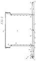
- An armored metal box 1 may be polygonal or cylindrical, and according to the preferred embodiment shown in Figs.1 and 2 is in the general form of a rectangular parallelepiped.
- the box contains integrated circuits and electronic components (not shown) which are preferably arranged on one and / or the other of the faces of several first printed cards 2 and which relate for example to a radio transmitter.
- the cards 2 are here stored parallel to two small vertical transverse walls 11 of the box and each slid into two slides fixed on the internal faces of two large vertical longitudinal walls 12 of the box.
- the walls 11 and 12 thus form a rectangular crown, the upper opening of which is closed by a horizontal metal cover 13 and the lower opening of which is closed by a horizontal base 3 according to the invention, constituting the bottom of the box.
- the crown 11-12, the cover 13 and a metal frame 4 in the base 3 are made from folded and welded sheets.
- the cover 13 is fixed to the crown 11-12 and the crown is fixed to the base 3 by means of screws 8 passing through upper and lower support flanges 16 on the outer edges of the openings of the crown in order to constitute a completely closed, shielded and preferably airtight enclosure.
- the cover 13 may include, on an external face, a finned cooling radiator. Under an internal face of the cover 13 can be provided a compressible thermoconductive mattress, preferably made of elastomer and charged with metallic particles, in order to constitute at the same time a thermal drain between the printed cards 2 internal to the box and the outside, and a means to press the printed cards against the bottom of the box and immobilize them in the enclosure 11-12-13 of the box.
- a compressible thermoconductive mattress preferably made of elastomer and charged with metallic particles
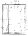
- the box base 3 essentially comprises the metal frame 4 and a second printed board 5, called the motherboard.
- the frame 4 is rectangular and thin. It has a flat bottom 40 significantly larger than the basic section, here horizontal, of the crown 11-12 of the box.
- the bottom 40 forms the seat of the cabinet.
- Four vertical sides 41 and 42 having a very small height relative to that of the box are erected perpendicular to the bottom 40 by folding sheet metal and are welded together in the corners of the frame, possibly reinforced by angles.
- the length of the frame 4 between the parallel sides 41 is substantially equal to the length of the crown between the walls 11, preferably substantially greater than the length of the crown, as will be seen below with reference to the Fig.5; the width of the frame 40 between the parallel sides 42 is significantly greater than the width of the crown between the walls 12 in order to provide a range 6 shown in Fig.1, or two ranges 6 shown in Fig.2, on the base 3 laterally to the enclosure 11-12-13 to fix standard electrical connectors 7.
- the connectors 7 are intended to connect external transmission lines or buses to the box, to the printed boards 2 through the motherboard 5 .
- the motherboard 5 is a double-sided printed board and preferably multilayer.
- the upper face 51 of the motherboard external to the base 3 is at least metallized completely in the areas 6 not covered by the enclosure 11-12-13.
- a rectangular lateral border 61 of the pads 6 is located below the longitudinal walls 12 of the box ring and, in a variant not shown, is also located below at least one of the transverse ring walls 11, when the length of the crown 11-12 is substantially smaller than that of the frame 4. More specifically, the edge 61 is in electrical and mechanical contact with the lower edges 16 of the metal crown in order to achieve perfect continuity of the shielding between the areas 6 and 1 enclosure 11-12-13 formed by the crown and the cover and containing the "daughter cards" 2.
- the external face 51 of the motherboard can be entirely metallized, including inside the enclosure 11-12-13.
- the metallized areas 6 are preferably covered with a insulating layer 62, such as epoxy resin, with the exception of the edge 61, in particular when the connectors 7 have lower faces applied to the motherboard which are metallic.
- a insulating layer 62 such as epoxy resin
- the motherboard 5 has a perimeter similar to that of the base frame 4, and here has a rectangular contour substantially smaller than the internal perimeter defined by the four sides of the frame 41 and 42, so that the motherboard closes the upper opening of the frame 4.
- small angles 43 are provided in overhang over the entire internal periphery of the frame 4.
- Horizontal wings 44 of the angles 43 are attached to the internal faces of the four sides of the frame 41 and 42 by continuous weld beads.
- the angles 43 support an electrical shielding joint 45, preferably flexible, such as a metallic braid.
- the joint 45 is continuous and forms a closed rectangle.
- the height of the seal 45 is greater than the vertical wing of the angles 43 so that, when the motherboard is inserted into the frame 4, the peripheral edge of the lower face 52 of the motherboard rests only on the seal 45, in excellent mechanical and electrical contact with it, whatever the clearance and the dimensional tolerances between the periphery of the motherboard 5 and the internal perimeter of the frame 4.
- the electrical continuity of the shielding between the metallized external areas 6 and the seal 45 is ensured by a rectangular metallized border 53 printed on the periphery of the lower face 52 of the motherboard 5 internal to the base 3 and by metallized holes 54 made in the motherboard and connecting the edge 53 to the pads 6.
- Discrete electrical components such as surge arresters and fuses, can be fixed to the motherboard and arranged in the space internal to the base, between the board- mother 5 and the bottom of the frame 40.
- the lower metallic border 53 is applied against the joint 45 under a substantial pressure exerted by the screwing of slotted head screws 8.
- the screws 8 pass through smooth second holes 55 made in the motherboard 5.
- holes 46 tapped in small cylindrical drums 47 which are brought back by welding on the internal face of the frame bottom 40, the screws 8 are screwed until the heads of the via 8 are applied against the upper face 51 of the motherboard.
- the height of the drums is less than the distance between the seal 45, including its thickness, and the internal face of the frame bottom 40, so that the underside of the motherboard 52 does not come into contact with the drums 47 and therefore the shielding edge 53 rests on the seal 45. In this case, the seal 45 is compacted to adhere to the angles 43 and to the frame sides 41 and 42.
- Tapped cylindrical drums 47 are also provided under the metal edge of the beach 61 in order to receive fixing screws 8 therefrom the lower edges 16 of the crown 11-12.
- At least one of the walls of the enclosure of the cabinet is arranged in line with the junction gap IJ between the corresponding side 41 of the frame 4 and the corresponding edge 55 of the motherboard 5, facing each other.
- said gap IJ has a width substantially equal to the thickness of the wall 11.
- the height of the wall 11 is greater than that of the walls 12 with flanges 16, and exceeds this by a length greater than the thickness of the motherboard 5 but less than the distance between the external face 51 of the motherboard and the wings 44 of the angles 43 supporting the electrical seal 5.
- the lower edge 110 of the wall 11 is substantially wedged between the frame 4 and the motherboard 5, and is in mechanical and electrical contact with the electrical seal 45, which improves the shielding.
- the box 1 constitutes a true Faraday cage, the electrical shielding continuity of which is perfectly ensured between the walls 11 and 12 of the enclosure containing the daughter cards 2 and the frame 4 of the base 3 through the tracks 6, the holes 54, the edge 53, and the joint 45 and the angles 43, while allowing easy disassembly and accessibility of the motherboard 5 supporting the external connectors 7.
Landscapes
- Engineering & Computer Science (AREA)
- Microelectronics & Electronic Packaging (AREA)
- Shielding Devices Or Components To Electric Or Magnetic Fields (AREA)
- Casings For Electric Apparatus (AREA)
- Packages (AREA)
Claims (9)
- Unterteil für ein abgeschirmtes Gehäuse (1), aufweisend einen metallischen Behälter (11-12-13), der elektronische Bauteile (2) enthält,- wobei das Unterteil (3) eine Leiterplatte (5) zur Verbindung der Bauteile (2) mit Verbindungsmitteln (7) und einen metallischen Rahmen (4) umfaßt,- wobei die Karte (5) auf einer Außenseite (51) wenigstens einen Bereich (6) aufweist, der metallisiert ist und sich auf der Außenseite des Behälters (11-12-13) befindet und der die Verbindungsmittel (7) trägt, und- wobei der metallische Rahmen (4) die Karte (5) einrahmende Seiten und einen die Grundplatte des Gehäuses bildenden Boden (40) umfaßt,gekennzeichnet durch eine elektrische Verbindung (45), die durch die Rahmenseiten (41, 42) gehaltert ist, und durch eine Einfassung (53), die auf einer Innenseite (52) der Karte (5) metallisiert ist, die elektrisch mit dem Bereich (6) auf der Außenseite verbunden ist und die gegen die elektrische Verbindung (45) angelegt ist.
- Unterteil nach Anspruch 1, dadurch gekennzeichnet, daß die elektrische Verbindung (45) ein Metallgeflecht ist.
- Unterteil nach Anspruch 2 oder 3, dadurch gekennzeichnet, daß es Metallwinkel (43) umfaßt, die gegen die Innenseiten der Seiten (41, 42) des Rahmens (4) aufgesetzt sind und die elektrische Verbindung (45) haltern.
- Unterteil nach einem beliebigen der Ansprüche 1 bis 3, gekennzeichnet durch metallisierte Löcher (54), die in der Karte (5) ausgeführt sind und die den Bereich (6) auf der Außenseite der Karte mit der Einfassung (53) auf der Innenseite der Karte verbinden.
- Unterteil nach einem beliebigen der Ansprüche 1 bis 4, gekennzeichnet durch mit Innengewinde versehene Hülsen, die auf dem Boden des Rahmens (40) ausgeführt sind, um die Karte (5) durchquerende Schrauben (8) aufzunehmen, und die die Karte auf der elektrischen Verbindung (45) festhalten.
- Unterteil nach einem beliebigen der Ansprüche 1 bis 5, gekennzeichnet durch eine völlig metallisierte Außenseite (51) der Karte (5).
- Unterteil nach einem beliebigen der Ansprüche 1 bis 6, gekennzeichnet durch eine Isolierschicht (62), die wenigstens den metallisierten Außenseitenbereich (6) bis zur Außenseite des Behälters (11, 12-13) überdeckt.
- Unterteil nach einem beliebigen der Ansprüche 1 bis 7, gekennzeichnet durch eine Inneneinfassung (61) des Außenseitenbereichs (6) im elektrischen und mechanischen Kontakt mit Randbereichen (16) des Gehäuses (11-12-13).
- Unterteil nach einem beliebigen der Ansprüche 1 bis 8, gekennzeichnet durch einen Zwischenraum (IJ) zwischen einer Seite (41) des Rahmens (4) und einer Kante (55) der Karte (5) gegenüber der Seite (41) für das teilweise Hindurchtreten einer Wand (11) des Gehäuses, deren Rand (110) sich in Kontakt mit der elektrischen Verbindung (45) befindet.
Applications Claiming Priority (2)
| Application Number | Priority Date | Filing Date | Title |
|---|---|---|---|
| FR9014308A FR2669501B1 (fr) | 1990-11-16 | 1990-11-16 | Embase pour coffret blinde de cartes imprimees. |
| FR9014308 | 1990-11-16 |
Publications (2)
| Publication Number | Publication Date |
|---|---|
| EP0486398A1 EP0486398A1 (de) | 1992-05-20 |
| EP0486398B1 true EP0486398B1 (de) | 1995-02-01 |
Family
ID=9402288
Family Applications (1)
| Application Number | Title | Priority Date | Filing Date |
|---|---|---|---|
| EP91403062A Expired - Lifetime EP0486398B1 (de) | 1990-11-16 | 1991-11-14 | Unterteil für ein abgeschirmtes Gehäuse mit elektronischen Schaltungen |
Country Status (4)
| Country | Link |
|---|---|
| EP (1) | EP0486398B1 (de) |
| AT (1) | ATE118150T1 (de) |
| DE (1) | DE69107174T2 (de) |
| FR (1) | FR2669501B1 (de) |
Families Citing this family (1)
| Publication number | Priority date | Publication date | Assignee | Title |
|---|---|---|---|---|
| ES2122491T3 (es) * | 1995-02-24 | 1998-12-16 | Hewlett Packard Co | Dispositivo para impedir interferencias electromagneticas. |
Family Cites Families (4)
| Publication number | Priority date | Publication date | Assignee | Title |
|---|---|---|---|---|
| GB1462058A (en) * | 1973-10-19 | 1977-01-19 | Microwave & Electronic Syst | Radio frequency screening and means therefor |
| DE2813812A1 (de) * | 1978-03-31 | 1979-10-04 | Hartmann & Braun Ag | Anordnung zur aufnahme von einschiebbaren elektrischen oder elektronischen baugruppen |
| US4717791A (en) * | 1986-07-09 | 1988-01-05 | Tektronix, Inc. | Shield structure for limiting transmission of electromagnetic radiation |
| US4868716A (en) * | 1988-07-15 | 1989-09-19 | Hewlett-Packard Company | RF interconnect and shielding system |
-
1990
- 1990-11-16 FR FR9014308A patent/FR2669501B1/fr not_active Expired - Fee Related
-
1991
- 1991-11-14 EP EP91403062A patent/EP0486398B1/de not_active Expired - Lifetime
- 1991-11-14 DE DE69107174T patent/DE69107174T2/de not_active Expired - Fee Related
- 1991-11-14 AT AT91403062T patent/ATE118150T1/de not_active IP Right Cessation
Also Published As
| Publication number | Publication date |
|---|---|
| ATE118150T1 (de) | 1995-02-15 |
| FR2669501A1 (fr) | 1992-05-22 |
| DE69107174D1 (de) | 1995-03-16 |
| FR2669501B1 (fr) | 1996-06-21 |
| EP0486398A1 (de) | 1992-05-20 |
| DE69107174T2 (de) | 1995-06-22 |
Similar Documents
| Publication | Publication Date | Title |
|---|---|---|
| FR2711454A1 (fr) | Liaison d'angle pour armoire, et armoire électrique comportant de telles liaisons. | |
| CA2075753C (fr) | Joint d'etancheite, notamment d'etancheite electromagnetique | |
| EP1087652A1 (de) | Verbesserungen für gekühlte elektronische Baugruppen, insbesondere für Steuerungsmodul eines Kraftfahrzeugscheinwerfers | |
| FR2595898A1 (fr) | Unite enfichable | |
| EP0486398B1 (de) | Unterteil für ein abgeschirmtes Gehäuse mit elektronischen Schaltungen | |
| CA1051966A (fr) | Piece d'assemblage | |
| FR2695287A1 (fr) | Appareil électrique, en particulier appareil de branchement et de commande pour véhicules à moteur. | |
| FR2656494A1 (fr) | Dispositif de blindage et d'isolation d'une carte de circuit electronique. | |
| FR2700093A1 (fr) | Ensemble électronique fait de deux cartes réunies par des moyens d'assemblage et matériel électronique comportant au moins un tel ensemble. | |
| FR2522872A1 (fr) | Transformateur de secteur | |
| FR2897927A1 (fr) | Carter, notamment pour appareil de chauffage, ventilation ou climatisation | |
| FR2571922A1 (fr) | Chassis etanche aux perturbations electromagnetiques et joint electromagnetique | |
| FR2982454A1 (fr) | Boitier electrique ou electronique destine a etre monte sur une structure presentant des irregularites de surface | |
| FR2511189A1 (fr) | Relais electromagnetique | |
| FR2972720A1 (fr) | Trappe coulissante, notamment pour element de stockage | |
| EP0411226A1 (de) | Verteilungsgehäuse | |
| FR2553839A1 (fr) | Dispositif pour assemblage d'etageres | |
| FR2819940A1 (fr) | Procede de fabrication d'un boitier semi-conducteur optique et boitier semi-conducteur optique | |
| FR2914118A1 (fr) | Pilier d'angle pour coffret electrique et coffret ainsi equipe | |
| CA2680494A1 (fr) | Boite aux lettres, livrable en kit | |
| FR2740936A1 (fr) | Ensemble compose d'un chassis et d'un capot de protection | |
| FR2956558A1 (fr) | Module electronique a dissipation thermique amelioree | |
| FR2671935A1 (fr) | Boitier de circuit electronique de puissance. | |
| JP2007181279A (ja) | 電気接続箱 | |
| FR2497565A1 (fr) | Caisson modulaire pour echangeur a flux croises |
Legal Events
| Date | Code | Title | Description |
|---|---|---|---|
| PUAI | Public reference made under article 153(3) epc to a published international application that has entered the european phase |
Free format text: ORIGINAL CODE: 0009012 |
|
| AK | Designated contracting states |
Kind code of ref document: A1 Designated state(s): AT BE CH DE DK ES GB GR IT LI LU NL SE |
|
| 17P | Request for examination filed |
Effective date: 19920516 |
|
| 17Q | First examination report despatched |
Effective date: 19940302 |
|
| GRAA | (expected) grant |
Free format text: ORIGINAL CODE: 0009210 |
|
| ITF | It: translation for a ep patent filed | ||
| AK | Designated contracting states |
Kind code of ref document: B1 Designated state(s): AT BE CH DE DK ES GB GR IT LI LU NL SE |
|
| PG25 | Lapsed in a contracting state [announced via postgrant information from national office to epo] |
Ref country code: NL Effective date: 19950201 Ref country code: GR Free format text: LAPSE BECAUSE OF FAILURE TO SUBMIT A TRANSLATION OF THE DESCRIPTION OR TO PAY THE FEE WITHIN THE PRESCRIBED TIME-LIMIT Effective date: 19950201 Ref country code: ES Free format text: THE PATENT HAS BEEN ANNULLED BY A DECISION OF A NATIONAL AUTHORITY Effective date: 19950201 Ref country code: DK Effective date: 19950201 Ref country code: AT Effective date: 19950201 |
|
| REF | Corresponds to: |
Ref document number: 118150 Country of ref document: AT Date of ref document: 19950215 Kind code of ref document: T |
|
| REF | Corresponds to: |
Ref document number: 69107174 Country of ref document: DE Date of ref document: 19950316 |
|
| PG25 | Lapsed in a contracting state [announced via postgrant information from national office to epo] |
Ref country code: SE Effective date: 19950501 |
|
| GBT | Gb: translation of ep patent filed (gb section 77(6)(a)/1977) |
Effective date: 19950406 |
|
| NLV1 | Nl: lapsed or annulled due to failure to fulfill the requirements of art. 29p and 29m of the patents act | ||
| PG25 | Lapsed in a contracting state [announced via postgrant information from national office to epo] |
Ref country code: LU Free format text: LAPSE BECAUSE OF NON-PAYMENT OF DUE FEES Effective date: 19951130 Ref country code: LI Effective date: 19951130 Ref country code: CH Effective date: 19951130 Ref country code: BE Effective date: 19951130 |
|
| PLBE | No opposition filed within time limit |
Free format text: ORIGINAL CODE: 0009261 |
|
| STAA | Information on the status of an ep patent application or granted ep patent |
Free format text: STATUS: NO OPPOSITION FILED WITHIN TIME LIMIT |
|
| 26N | No opposition filed | ||
| BERE | Be: lapsed |
Owner name: SOC. ANONYME DE TELECOMMUNICATIONS SAT Effective date: 19951130 |
|
| REG | Reference to a national code |
Ref country code: CH Ref legal event code: PL |
|
| PGFP | Annual fee paid to national office [announced via postgrant information from national office to epo] |
Ref country code: DE Payment date: 20001019 Year of fee payment: 10 |
|
| PGFP | Annual fee paid to national office [announced via postgrant information from national office to epo] |
Ref country code: GB Payment date: 20011106 Year of fee payment: 11 |
|
| REG | Reference to a national code |
Ref country code: GB Ref legal event code: IF02 |
|
| PG25 | Lapsed in a contracting state [announced via postgrant information from national office to epo] |
Ref country code: DE Free format text: LAPSE BECAUSE OF NON-PAYMENT OF DUE FEES Effective date: 20020702 |
|
| PG25 | Lapsed in a contracting state [announced via postgrant information from national office to epo] |
Ref country code: GB Free format text: LAPSE BECAUSE OF NON-PAYMENT OF DUE FEES Effective date: 20021114 |
|
| GBPC | Gb: european patent ceased through non-payment of renewal fee | ||
| PG25 | Lapsed in a contracting state [announced via postgrant information from national office to epo] |
Ref country code: IT Free format text: LAPSE BECAUSE OF NON-PAYMENT OF DUE FEES Effective date: 20051114 |