EP0486231A2 - Paralleles Verarbeitungssystem - Google Patents
Paralleles Verarbeitungssystem Download PDFInfo
- Publication number
- EP0486231A2 EP0486231A2 EP91310355A EP91310355A EP0486231A2 EP 0486231 A2 EP0486231 A2 EP 0486231A2 EP 91310355 A EP91310355 A EP 91310355A EP 91310355 A EP91310355 A EP 91310355A EP 0486231 A2 EP0486231 A2 EP 0486231A2
- Authority
- EP
- European Patent Office
- Prior art keywords
- disk
- printed
- bus
- processing system
- signal conductor
- Prior art date
- Legal status (The legal status is an assumption and is not a legal conclusion. Google has not performed a legal analysis and makes no representation as to the accuracy of the status listed.)
- Withdrawn
Links
Images




Classifications
-
- G—PHYSICS
- G06—COMPUTING OR CALCULATING; COUNTING
- G06F—ELECTRIC DIGITAL DATA PROCESSING
- G06F15/00—Digital computers in general; Data processing equipment in general
- G06F15/16—Combinations of two or more digital computers each having at least an arithmetic unit, a program unit and a register, e.g. for a simultaneous processing of several programs
-
- G—PHYSICS
- G06—COMPUTING OR CALCULATING; COUNTING
- G06F—ELECTRIC DIGITAL DATA PROCESSING
- G06F13/00—Interconnection of, or transfer of information or other signals between, memories, input/output devices or central processing units
- G06F13/38—Information transfer, e.g. on bus
- G06F13/40—Bus structure
- G06F13/4063—Device-to-bus coupling
- G06F13/409—Mechanical coupling
-
- H—ELECTRICITY
- H05—ELECTRIC TECHNIQUES NOT OTHERWISE PROVIDED FOR
- H05K—PRINTED CIRCUITS; CASINGS OR CONSTRUCTIONAL DETAILS OF ELECTRIC APPARATUS; MANUFACTURE OF ASSEMBLAGES OF ELECTRICAL COMPONENTS
- H05K1/00—Printed circuits
- H05K1/02—Details
- H05K1/14—Structural association of two or more printed circuits
-
- H—ELECTRICITY
- H05—ELECTRIC TECHNIQUES NOT OTHERWISE PROVIDED FOR
- H05K—PRINTED CIRCUITS; CASINGS OR CONSTRUCTIONAL DETAILS OF ELECTRIC APPARATUS; MANUFACTURE OF ASSEMBLAGES OF ELECTRICAL COMPONENTS
- H05K7/00—Constructional details common to different types of electric apparatus
- H05K7/14—Mounting supporting structure in casing or on frame or rack
- H05K7/1438—Back panels or connecting means therefor; Terminals; Coding means to avoid wrong insertion
- H05K7/1439—Back panel mother boards
- H05K7/1442—Back panel mother boards with a radial structure
Definitions
- the present invention relates to an improvement in or relating to a parallel processing system which permits the simultaneous operation of a plurality of processing units such as processors or memories, thereby attaining the high-speed processing of data, particularly color image data.
- Fig.11 shows a conventional parallel processing system comprising a plurality of processing units 1 to 6 connected to each other via buses.
- Fig.12 shows another conventional parallel processing system comprising a plurality of processing units 1 to 6 connected via a crossbar switch.
- the perpetual connection type of parallel processing system as shown in Fig.11 requires means to compensate for time difference in transporting data between different processing units due to different lengths of bus conductors between different processing units. Accordingly such parallel processing system is complicated, and the high-speed data transportation, and hence the high-speed data processing is hardly attainable.
- the number of the contacts of the crossbar switch will increase with the increase of the processing units to be handled. This will increase the size and cost of the whole system, and still disadvantageously data transportation distance will increase.
- the elongation of bus conductors is the cause for producing noise signals, and at the same time, making the data network sensitive to external noise signals.
- a parallel processing system comprises a stack assembly of bus-printed disks whose centres are arranged on a common centre axis, and a plurality of processing unit boards standing upright around and electrically connected to the stack assembly of bus-printed disks, wherein each bus-printed disk comprises a disk of dielectric material bearing a printed radial pattern including a plurality of printed signal conductors of substantially equal length radially extending from the centre of the disk, the signal conductors being connected in pairs; an integrated circuit, crossbar switch placed at the centre of the disk, the terminals of the crossbar switch being connected to the plurality of printed signal pairs; a plurality of impedance matching elements one connected to each signal conductor pair; and means to connect each of the impedance matching elements to a selected lead in a selected one of the processing unit boards, and at least one of the processing unit boards having means for controlling all the integrated circuit crossbar switches to allow the switch elements of each crossbar switch to open and close in a predetermined sequence.
- the radial printed signal conductor pairs at equi-phase positions of all the disks make up parallel buses, and these parallel buses will be used as data lines, address lines, control lines etc.
- the contacts of the switching elements of every crossbar switch are controlled so as to open and close in a predetermined sequence.
- the processing units such as processors, memories etc can be selectively simultaneously connected via closed switching elements and associated transmission lines, thereby permitting selected processing units to send and receive data and effect data processing as required.
- the radial signal conductors are of equal length, and therefore the transmission distance and hence transmission time is equal regardless of which processing units may be selected and connected.
- the terminating of each signal conductor with an impedance matching element has the effect of preventing the reflection of signals in the transmission line. Thus, a high-speed, reliable data transmission is permitted.
- the stacking of radial signal conductor arrangements along a common center axis permits reduction of conductor length no matter how many processing units may be used in combination. Reduction of transmission lengths will prevent appearance of noise signals, and at the same time, will be insensitive to exterior noise signals, and still advantageously will lead to reduction of the size of the whole system and enable high speed data processing free from transmission errors.
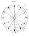
- a bus printed disk 7 comprises a disk of dielectric material 8 bearing on each of its opposite major surfaces, a printed radial pattern including a plurality of printed signal conductors 13 or 15 of equal length radially extending from the center of the disk, and an integrated circuit crossbar one 9 placed on the center of one major surface of the disk 8.
- the crossbar switch 9 comprises a grid network having switching contacts 11 one at each crossing of signal conductors 10 and terminals 12 connected to signal conductors 10, as seen from Fig.5.
- the printed signal conductors 13 on the front surface of the disk 8 radially extend from the crossbar switch 9 at regular angular intervals with their inner ends connected to the terminals 12 of the crossbar switch 9.
- the printed signal conductors 15 on the back surface of the disk 8 radially extend from the center 14 of the disk 8 at the same angular intervals as the front surface.
- Each signal conductor 13 on the front surface is connected to a corresponding signal conductor 15 on the back surface to make up a signal conductor pair;
- the outer or distal ends of the signal conductors 13 on the front surface of the disk 8 are connected to terminals 17, which are fixed to the circumference of the disk 8 at regular intervals, via the resistors R1 of the matchingcircuits 16.
- a printed resistor or chip resistor may be used as R1.
- the outer or distal ends of the signal conductors 15 on the back surface of the disk 8 are connected to annular ground conductor 18 via the resistors R1 of the matching circuits 16 as shown in Fig.2.
- the annular ground conductor 18 is connected to land pieces 20 on the front surface of the disk 8 through plated through holes 19. Each land piece 20 is connected to an associated terminal via the resistor R2 of the impedance matching circuit 16, as seen from Figs. 3 and 4.
- a printed resistor or chip resistor may be used as R2.
- the crossbar switch 9 has a plurality of control terminals 21 other than the exterior terminals 12, and control conductors 22 are connected to these control terminals 21, although single control terminal and control conductor are shown in Fig.1 only for the sake of simplicity in the drawing.
- a plurality of bus printed disks 7 are arranged vertically at regular intervals along a common center axis with their signal conductor pairs 13, 15 and control conductors 22 vertically aligned in registration.
- each vertical alignment of radial signal conductor pairs 13, 15 in registration constitutes a parallel bus.
- the parallel buses thus constituted may be used as data lines, address lines, control lines etc.
- Printed boards 24 each equipped with a processing unit 23 are arranged around the stack assembly of bus printed disks 7 in radial directions, as shown in Fig.7. Exterior terminals 25 of each printed board 24 are electrically connected to the terminals 17 of the bus printed disks 7 via associated connectors ( not shown ). As shown in Fig.3, each terminal 17 on the dielectric disk 8 has an outward opening tube receptacle 26, and each exterior terminal 25 on the bus printed disk 7 has a male plug (not shown ) to insert in a corresponding receptacle 26.
- At least one of the processing unit boards 24 has a crossbar switch controller 27 for controlling all the integrated circuit crossbar switches 9 to allow the switch elements 11 of each crossbar switch to open and close in a predetermined sequence, as described later.
- Examples of the processing units 23 to be mounted to printed boards 24 are processors (abbreviated CPU ), memories, input/output processors to control keyboards, displays etc.
- processors abbreviated CPU
- memories abbreviated RAM
- input/output processors to control keyboards, displays etc.
- Fig.8 shows an equivalent circuit of a single transmission line constituted by signal conductors 13 and 15 on a bus printed disk 7 for high frequency signals.
- C1 stands for a parasitic capacitor appearing across the resistor R1
- C2 stands for a parasitic capacitor appearing between signal conductors 13 and 15 on the opposite surfaces of the disk 7.
- resistors R1 and R2 can be determined on the assumption just described and in consideration of the characteristic impedance of the transmission line and other circuit factors.
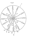
- Fig.9 shows another bus-printed disk 71 having twisted signal conductors 131 and 151 radiating from its center.
- a disk of dielectric material has a plurality of plated through holes 50 made at intervals along each radial line, and each signal conductor pair comprises two conductors 131 ( front surface ) and 151 ( back surface ) passing through every other hole 50 to alternately appear on front or back surface of the disk, thus making up twisted signal conductors of equal length.
- Twisted signal conductors are terminated with the two resistors R11 which are parts of an impedance matching circuit 16.
- the twisting of the signal conductors 13 and 15 on the opposite surfaces of the disk has the effect of reducing undesired electrostatic or magnetic inductions; making the transmission lines less sensitive to exterior noise signals; and preventing undesired electromagnetic radiation from the transmission lines.
- a parallelizing compiler will find out which parts of the program can be parallel-performed, and then it will rearrange such parts in parallel tasks.
- a parallel language compiler will selectively pick up parallel parts so that parallel machine codes may be prepared.
- the operating system of parallel machine will carry out dynamic allotment of processors, and the switching controlling schedule of each crossbar switch will be prepared on the basis of the allotment of processors. In this way parallel-processing will be handled.
- the crossbar switch controller 27 performs the switching of all crossing contacts 11 in each crossbar switch 9 according to the schedule, thereby permitting all processing units 23 to carry out simultaneously the processing of data.
- Bus printed disks 7 are shown as having printed patterns on both sides. However, use may be made of a multi-layered disk having signal conductors printed on each layer. The use of such multi-layered disks makes it possible to substantially increase the density and compactness of elements in a parallel processing system, and accordingly reduce the size of the parallel processing system.
- a parallel processing system In the case where a parallel processing system according to the present invention is used in processing color-image data and outputting the processed data to a display device, red, green and blue data retrieved from different memories are further processed, and then the processed data are further transported to selected 1/0 CPUs by controlling the crossbar switch of the parallel-processing system, thus omitting transportation of data between memories.
- a parallel processing system uses a pile of bus disks each having an integrated circuit crossbar switch at its center and a plurality of signal conductors radiating from the center crossbar switch, thus providing communication lines of equal, shortest possible length to make a required electrical connection between selected processing units, no matter how many processing units may be used. Also, the terminating of each signal conductor with an impedance matching circuit permits suppression of reflection of signals at the end of signal conductor. Thus, reliable, noise-free, high-speed transportation of data is permitted.
Landscapes
- Engineering & Computer Science (AREA)
- Theoretical Computer Science (AREA)
- General Engineering & Computer Science (AREA)
- Computer Hardware Design (AREA)
- Microelectronics & Electronic Packaging (AREA)
- Physics & Mathematics (AREA)
- General Physics & Mathematics (AREA)
- Software Systems (AREA)
- Multi Processors (AREA)
Applications Claiming Priority (4)
| Application Number | Priority Date | Filing Date | Title |
|---|---|---|---|
| JP308848/90 | 1990-11-16 | ||
| JP2308848A JPH04181410A (ja) | 1990-11-16 | 1990-11-16 | 並列処理装置 |
| JP325038/90 | 1990-11-26 | ||
| JP2325038A JPH04191956A (ja) | 1990-11-26 | 1990-11-26 | 並列処理装置 |
Publications (2)
| Publication Number | Publication Date |
|---|---|
| EP0486231A2 true EP0486231A2 (de) | 1992-05-20 |
| EP0486231A3 EP0486231A3 (en) | 1993-05-12 |
Family
ID=26565704
Family Applications (1)
| Application Number | Title | Priority Date | Filing Date |
|---|---|---|---|
| EP19910310355 Withdrawn EP0486231A3 (en) | 1990-11-16 | 1991-11-08 | Parallel processing system |
Country Status (6)
| Country | Link |
|---|---|
| US (1) | US5341509A (de) |
| EP (1) | EP0486231A3 (de) |
| KR (1) | KR920010474A (de) |
| AU (1) | AU8790791A (de) |
| CA (1) | CA2055078A1 (de) |
| IL (1) | IL99978A0 (de) |
Cited By (1)
| Publication number | Priority date | Publication date | Assignee | Title |
|---|---|---|---|---|
| EP0958717A4 (de) * | 1996-04-15 | 2002-07-24 | Arizona Digital Inc | Rückwand für hochgeschwindigkeits-datenverarbeitungssystem |
Families Citing this family (12)
| Publication number | Priority date | Publication date | Assignee | Title |
|---|---|---|---|---|
| US5519584A (en) * | 1994-12-22 | 1996-05-21 | At&T Corp. | Laminated cylindrical backplane |
| US6404299B1 (en) * | 1998-07-31 | 2002-06-11 | Russound/Fmp, Inc. | Devices, methods, and systems for network hub partial termination |
| US20060174052A1 (en) * | 2005-02-02 | 2006-08-03 | Nobukazu Kondo | Integrated circuit and information processing device |
| JP3625260B2 (ja) * | 1999-08-12 | 2005-03-02 | 富士通株式会社 | 回線モジュールプロテクション方法及びそれを用いた装置 |
| JP4397109B2 (ja) * | 2000-08-14 | 2010-01-13 | 富士通株式会社 | 情報処理装置及びクロスバーボードユニット・バックパネル組立体の製造方法 |
| US6625000B2 (en) * | 2000-10-21 | 2003-09-23 | Current Technology, Inc. | Modular structures for transient voltage surge suppressors |
| DE10130592C1 (de) * | 2001-06-27 | 2002-10-24 | Infineon Technologies Ag | Modulbaugruppe für Speicher-Module und Verfahren zu ihrer Herstellung |
| US8023280B2 (en) * | 2003-07-28 | 2011-09-20 | Qualcomm Incorporated | Communication circuit for driving a plurality of devices |
| WO2006076381A2 (en) * | 2005-01-12 | 2006-07-20 | Legacy Electronics, Inc. | Radial circuit board, system, and methods |
| CN101622606B (zh) * | 2006-12-06 | 2014-04-09 | 弗森-艾奥公司 | 用于作为大容量、非易失性存储器的高速缓存的固态存储器的装置、系统和方法 |
| WO2009032144A2 (en) * | 2007-08-28 | 2009-03-12 | General Dynamics Advanced Information Systems, Inc. | System and method for interconnecting circuit boards |
| US20240314930A1 (en) * | 2023-03-14 | 2024-09-19 | Samsung Electronics Co., Ltd. | Computing system with connecting boards |
Family Cites Families (11)
| Publication number | Priority date | Publication date | Assignee | Title |
|---|---|---|---|---|
| US4331956A (en) * | 1980-09-29 | 1982-05-25 | Lovelace Alan M Administrator | Control means for a solid state crossbar switch |
| US4456965A (en) * | 1980-10-14 | 1984-06-26 | Texas Instruments Incorporated | Data processing system having multiple buses |
| CH664662A5 (en) * | 1986-02-26 | 1988-03-15 | Valtronic S A | Interconnecting device for electronic cards in star formation - has upright around insulating central core contg. conductive connectors for mating with edge connectors |
| US4734825A (en) * | 1986-09-05 | 1988-03-29 | Motorola Inc. | Integrated circuit stackable package |
| US4908576A (en) * | 1987-09-08 | 1990-03-13 | Jackson Daniel K | System for printed circuit board testing |
| US4985830A (en) * | 1988-09-27 | 1991-01-15 | Universities Research Association, Inc. | Interprocessor bus switching system for simultaneous communication in plural bus parallel processing system |
| US5189665A (en) * | 1989-03-30 | 1993-02-23 | Texas Instruments Incorporated | Programmable configurable digital crossbar switch |
| JP2591677B2 (ja) * | 1989-04-21 | 1997-03-19 | 株式会社 グラフィコ | 放射型・パラレル・システムバス |
| JP2626698B2 (ja) * | 1989-06-15 | 1997-07-02 | 株式会社 グラフィコ | 放射型・パラレル・システムバス |
| JPH0743699B2 (ja) * | 1990-07-09 | 1995-05-15 | 株式会社グラフィコ | 並列処理装置 |
| US5210682A (en) * | 1990-10-19 | 1993-05-11 | Graphico Co., Ltd. | Radial type of parallel system bus structure having pairs of conductor lines with impedance matching elements |
-
1991
- 1991-11-06 IL IL99978A patent/IL99978A0/xx unknown
- 1991-11-06 CA CA002055078A patent/CA2055078A1/en not_active Abandoned
- 1991-11-06 US US07/788,470 patent/US5341509A/en not_active Expired - Fee Related
- 1991-11-08 EP EP19910310355 patent/EP0486231A3/en not_active Withdrawn
- 1991-11-15 AU AU87907/91A patent/AU8790791A/en not_active Abandoned
- 1991-11-16 KR KR1019910020408A patent/KR920010474A/ko not_active Ceased
Cited By (1)
| Publication number | Priority date | Publication date | Assignee | Title |
|---|---|---|---|---|
| EP0958717A4 (de) * | 1996-04-15 | 2002-07-24 | Arizona Digital Inc | Rückwand für hochgeschwindigkeits-datenverarbeitungssystem |
Also Published As
| Publication number | Publication date |
|---|---|
| AU8790791A (en) | 1992-05-21 |
| CA2055078A1 (en) | 1992-05-17 |
| EP0486231A3 (en) | 1993-05-12 |
| IL99978A0 (en) | 1992-08-18 |
| US5341509A (en) | 1994-08-23 |
| KR920010474A (ko) | 1992-06-26 |
Similar Documents
| Publication | Publication Date | Title |
|---|---|---|
| US5301089A (en) | Parallel processing system | |
| US5700167A (en) | Connector cross-talk compensation | |
| US5341509A (en) | Parallel processing system including a stack of bus-printed disks and a plurality of radially exending processing unit boards | |
| KR100750038B1 (ko) | 디지털 전송 시스템들과 함께 사용하기 위한 소형 전자기커플러 | |
| US6805560B1 (en) | Apparatus interconnecting circuit board and mezzanine card or cards | |
| US4685032A (en) | Integrated backplane | |
| US5525067A (en) | Ground plane interconnection system using multiple connector contacts | |
| CA2347985C (en) | Crosstalk compensation for electrical connectors | |
| US6165018A (en) | Connector having internal crosstalk compensation | |
| EP0940850B1 (de) | Verbesserte Signalübertragung durch verlängerte Übertragungsleitungen bei 'DIMM' Speichermodulen | |
| EP0391527A1 (de) | Leiterplattenanordnung zur Reduzierung von Signalstörungen | |
| US5210682A (en) | Radial type of parallel system bus structure having pairs of conductor lines with impedance matching elements | |
| US3808566A (en) | Switching system | |
| US2951184A (en) | Printed wiring assembly | |
| US6349037B1 (en) | Backplane for common building block | |
| US6486746B1 (en) | Termination circuit for decoupling unused wires on a network device's unshielded twisted pair (UTP) cable | |
| JPS6367845A (ja) | 一定の電気特性を有するバス構造 | |
| US5269693A (en) | Connector for printed circuit boards | |
| EP0466394A2 (de) | Steckverbinderbaugruppe | |
| US5944541A (en) | Interleaved power and impedance control using daughtercard edge connector pin arrangement | |
| US20040210700A1 (en) | Compact PCI backplane and method of data transfer across the compact PCI backplane | |
| AU673386B2 (en) | LAN interface | |
| EP0520706A1 (de) | Integrierter Kreuzpunktschalter und paralleles Verarbeitungssystem unter Verwendung desselben | |
| US5652553A (en) | Signal transmission between modules connected to a common backplane | |
| US5674077A (en) | Interleaved connector circuit having increased backplane impedance |
Legal Events
| Date | Code | Title | Description |
|---|---|---|---|
| PUAI | Public reference made under article 153(3) epc to a published international application that has entered the european phase |
Free format text: ORIGINAL CODE: 0009012 |
|
| AK | Designated contracting states |
Kind code of ref document: A2 Designated state(s): AT BE CH DE DK ES FR GB GR IT LI LU NL SE |
|
| PUAL | Search report despatched |
Free format text: ORIGINAL CODE: 0009013 |
|
| AK | Designated contracting states |
Kind code of ref document: A3 Designated state(s): AT BE CH DE DK ES FR GB GR IT LI LU NL SE |
|
| 17P | Request for examination filed |
Effective date: 19931110 |
|
| STAA | Information on the status of an ep patent application or granted ep patent |
Free format text: STATUS: THE APPLICATION HAS BEEN WITHDRAWN |
|
| 18W | Application withdrawn |
Withdrawal date: 19940616 |