EP0484808A2 - Process and apparatus for selective metallisation - Google Patents
Process and apparatus for selective metallisation Download PDFInfo
- Publication number
- EP0484808A2 EP0484808A2 EP91118471A EP91118471A EP0484808A2 EP 0484808 A2 EP0484808 A2 EP 0484808A2 EP 91118471 A EP91118471 A EP 91118471A EP 91118471 A EP91118471 A EP 91118471A EP 0484808 A2 EP0484808 A2 EP 0484808A2
- Authority
- EP
- European Patent Office
- Prior art keywords
- substrate
- metal
- solution
- metallic layers
- organometallic compound
- Prior art date
- Legal status (The legal status is an assumption and is not a legal conclusion. Google has not performed a legal analysis and makes no representation as to the accuracy of the status listed.)
- Withdrawn
Links
Images
Classifications
-
- H—ELECTRICITY
- H05—ELECTRIC TECHNIQUES NOT OTHERWISE PROVIDED FOR
- H05K—PRINTED CIRCUITS; CASINGS OR CONSTRUCTIONAL DETAILS OF ELECTRIC APPARATUS; MANUFACTURE OF ASSEMBLAGES OF ELECTRICAL COMPONENTS
- H05K3/00—Apparatus or processes for manufacturing printed circuits
- H05K3/10—Apparatus or processes for manufacturing printed circuits in which conductive material is applied to the insulating support in such a manner as to form the desired conductive pattern
- H05K3/105—Apparatus or processes for manufacturing printed circuits in which conductive material is applied to the insulating support in such a manner as to form the desired conductive pattern by conversion of non-conductive material on or in the support into conductive material, e.g. by using an energy beam
-
- C—CHEMISTRY; METALLURGY
- C23—COATING METALLIC MATERIAL; COATING MATERIAL WITH METALLIC MATERIAL; CHEMICAL SURFACE TREATMENT; DIFFUSION TREATMENT OF METALLIC MATERIAL; COATING BY VACUUM EVAPORATION, BY SPUTTERING, BY ION IMPLANTATION OR BY CHEMICAL VAPOUR DEPOSITION, IN GENERAL; INHIBITING CORROSION OF METALLIC MATERIAL OR INCRUSTATION IN GENERAL
- C23C—COATING METALLIC MATERIAL; COATING MATERIAL WITH METALLIC MATERIAL; SURFACE TREATMENT OF METALLIC MATERIAL BY DIFFUSION INTO THE SURFACE, BY CHEMICAL CONVERSION OR SUBSTITUTION; COATING BY VACUUM EVAPORATION, BY SPUTTERING, BY ION IMPLANTATION OR BY CHEMICAL VAPOUR DEPOSITION, IN GENERAL
- C23C18/00—Chemical coating by decomposition of either liquid compounds or solutions of the coating forming compounds, without leaving reaction products of surface material in the coating; Contact plating
- C23C18/14—Decomposition by irradiation, e.g. photolysis, particle radiation or by mixed irradiation sources
- C23C18/143—Radiation by light, e.g. photolysis or pyrolysis
-
- H—ELECTRICITY
- H05—ELECTRIC TECHNIQUES NOT OTHERWISE PROVIDED FOR
- H05K—PRINTED CIRCUITS; CASINGS OR CONSTRUCTIONAL DETAILS OF ELECTRIC APPARATUS; MANUFACTURE OF ASSEMBLAGES OF ELECTRICAL COMPONENTS
- H05K3/00—Apparatus or processes for manufacturing printed circuits
- H05K3/10—Apparatus or processes for manufacturing printed circuits in which conductive material is applied to the insulating support in such a manner as to form the desired conductive pattern
- H05K3/12—Apparatus or processes for manufacturing printed circuits in which conductive material is applied to the insulating support in such a manner as to form the desired conductive pattern using thick film techniques, e.g. printing techniques to apply the conductive material or similar techniques for applying conductive paste or ink patterns
- H05K3/1241—Apparatus or processes for manufacturing printed circuits in which conductive material is applied to the insulating support in such a manner as to form the desired conductive pattern using thick film techniques, e.g. printing techniques to apply the conductive material or similar techniques for applying conductive paste or ink patterns by ink-jet printing or drawing by dispensing
- H05K3/125—Apparatus or processes for manufacturing printed circuits in which conductive material is applied to the insulating support in such a manner as to form the desired conductive pattern using thick film techniques, e.g. printing techniques to apply the conductive material or similar techniques for applying conductive paste or ink patterns by ink-jet printing or drawing by dispensing by ink-jet printing
-
- H—ELECTRICITY
- H05—ELECTRIC TECHNIQUES NOT OTHERWISE PROVIDED FOR
- H05K—PRINTED CIRCUITS; CASINGS OR CONSTRUCTIONAL DETAILS OF ELECTRIC APPARATUS; MANUFACTURE OF ASSEMBLAGES OF ELECTRICAL COMPONENTS
- H05K2201/00—Indexing scheme relating to printed circuits covered by H05K1/00
- H05K2201/03—Conductive materials
- H05K2201/0332—Structure of the conductor
- H05K2201/0335—Layered conductors or foils
- H05K2201/0347—Overplating, e.g. for reinforcing conductors or bumps; Plating over filled vias
-
- H—ELECTRICITY
- H05—ELECTRIC TECHNIQUES NOT OTHERWISE PROVIDED FOR
- H05K—PRINTED CIRCUITS; CASINGS OR CONSTRUCTIONAL DETAILS OF ELECTRIC APPARATUS; MANUFACTURE OF ASSEMBLAGES OF ELECTRICAL COMPONENTS
- H05K2203/00—Indexing scheme relating to apparatus or processes for manufacturing printed circuits covered by H05K3/00
- H05K2203/01—Tools for processing; Objects used during processing
- H05K2203/0104—Tools for processing; Objects used during processing for patterning or coating
- H05K2203/013—Inkjet printing, e.g. for printing insulating material or resist
-
- H—ELECTRICITY
- H05—ELECTRIC TECHNIQUES NOT OTHERWISE PROVIDED FOR
- H05K—PRINTED CIRCUITS; CASINGS OR CONSTRUCTIONAL DETAILS OF ELECTRIC APPARATUS; MANUFACTURE OF ASSEMBLAGES OF ELECTRICAL COMPONENTS
- H05K2203/00—Indexing scheme relating to apparatus or processes for manufacturing printed circuits covered by H05K3/00
- H05K2203/12—Using specific substances
- H05K2203/121—Metallo-organic compounds
Definitions
- the invention relates to a method and a device for producing partial metallic layers from a metal-containing, in particular organometallic compound on a substrate by irradiation with a light source.
- the invention is based on the object of specifying a method and a device for producing partial metallic layers with which structured metallizations can be applied to any substrate in a simple, environmentally friendly and economical manner.
- This object is achieved with respect to the method in that the metal-containing, in particular organometallic compound is applied to the surface of the substrate using a writing device in the form of a solution film which contains the metal-containing, in particular organometallic compound, and in that the metal-containing, in particular organometallic compound is then exposed to the action of UV photons of a defined wavelength.
- the object is achieved with respect to the device by means of a writing device which can be supplied with a solution containing a metal-containing, in particular organometallic compound on the input side and applies this solution to the substrate via a nozzle on the output side, the writing device and substrate being arbitrary in the XYZ direction against one another at high speeds are movable.
- Quartz, glass and silicon, light flexible plastics (Teflon, polyimides etc.) rubber, plastic or glass fleece, ceramic filled or glass fiber reinforced fluoroplastics, press boards and paper or cardboard with low temperature resistance can be produced. All substrate materials can be coated with the same good quality.
- the layers have good adhesive strength and electrical conductivity and are easily solderable and bondable.
- fine structure technology encompasses the creation of the finest conductor tracks and structures with very close spacings, as a result of which a high integration density is achieved. This allows components, e.g. Coils, solar cells, display cells etc., can be miniaturized. Such components with increased packing density are of interest for microelectronics in general, printed circuit board technology, hybrid and sensor technology and for decorative applications.
- the proposed method is relatively little time-consuming and very economical.
- the proposed device is user-friendly, inexpensive and fast in the production of fine structure technology on any substrate surface.
- the proposed method allows considerable savings to be made in the methods used. partly achieve expensive organometallic substances, since from the start only the areas to be metallized are wetted with the solvent film.
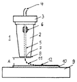
- a writing device 1 can be seen with a housing 2 with cover 3 and bottom 8, a pipe connection 4 in the cover 3 for the solution supply, a capillary 5 which extends from the pipe connection 4 to the nozzle 7 in the bottom 8 and with a piezoelectric transducer (transducer) 6, which encloses the capillary 5 and is used to express the solution from the nozzle 7.
- Impulse jets, thermal jets or aerosol jets can be used, with jet being a liquid jet.
- a fiber pen, a ballpoint pen, a fountain pen or an ink pen can also be used as writing instruments.
- the liquid drops 11 squeezed out of the nozzle 7 wet the substrate 10 arranged below the nozzle 7 of the writing device, as a result of which a "written" Structure 12 is formed on the substrate 10.
- the distance A between nozzle 7 and substrate 10 is preferably 1 mm.
- the substrate 10 is preferably fastened on a computer-controlled XYZ shift table 9, so that any desired structuring of the substrate 10 with solution is possible by shifting the table 9 in the X or Y or Z or in the X and Y and Z directions is.
- Simultaneous displacement of both the writing device 1 and the displacement table 9 with substrate 10 is also possible, as a result of which the structuring speed is further increased.
- a writing process with liquid, organometallic or other metal-containing compounds is therefore used in combination with the computer technology in order to write any structures such as conductor tracks, connections, coils, meanders etc. on any surfaces (line width, for example 50 ⁇ m ).
- Calculated metal patterns can be generated directly with computer-controlled writing devices.
- a scanning device line scanner
- Another advantage of computer technology in connection with the technology described is that the writing device over Data lines can be controlled remotely, and that several such writing devices can be controlled by a (possibly distant) computer.
- a central writing device can be operated by different computers.
- Organometallic and other metal-containing compounds are used as compounds, such as palladium acetate, palladium acetylacetonate, palladium chloride, cobalt acetate, nickel acetate, copper formate, silver neodecanates, cyclopentadienyl palladium allyl or cyclopentadienyl palladium chloride etc., which have strong absorption bands in the UV range from 60 nm to 400 nm.
- solvents e.g. Chloroform, alcohol, water and others used.
- the solution can be chloroform containing palladium acetate. It is also possible to dissolve cyclopentadienylpalladium allyl, which is in powder form, in alcohol or water and to apply it to the substrate. The use of powdered cyclopentadienyl palladium chloride, which is also dissolved in alcohol or water to form a solution, is also possible.
- the solutions are preferably applied to the substrate so thick that the metallic layer has a thickness between 0.5 and 50 nm.
- UV radiation is used in order to achieve the decomposition of the non-conductive organometallic compounds by exposing the thin organometallic layer structures and to effect a deposition of the corresponding metals (UV-assisted deposition of a catalyst from organometallic adsorbates on the substrate surface. Because this is ultraviolet The substrate material remains unaffected. The properties of the substrate material play only an insignificant role in the deposition process.
- An incoherent excimer light source with the desired wavelength is preferably used as the UV source. A detailed description of such a high-power radiator can be found in EP-OS 0 254 111.
- the high-performance radiator consists of a metal electrode cooled by a metal electrode and a dielectric or two dielectrics delimited and filled with a noble gas or gas mixture discharge space.
- the dielectric and the second electrode lying on the surface of the dielectric facing away from the discharge space are transparent to the radiation generated by the silent electrical discharge.
- a wavelength of 300 to 320 nm can be generated with the high-power radiator.
- the high-performance radiator works in quasi-pulsed operation. If the entire surface of the substrate to be coated is to be provided with a metal structure, a high-power radiator is used, the radiation field of which corresponds to the size of the substrate surface. The irradiation can be carried out for a few seconds up to a few minutes, depending on the circumstances, application thickness and distance between the substrate surface and the UV high-power lamp.
- a high-power mercury lamp can also be used for the formation of the metallic layers.
- the geometry of the UV high-power lamp or high-performance mercury lamp used can be adapted to the geometry of the substrates to be coated. It is quite possible, for example, that Carry out coating of rectangular substrates on a conveyor belt every second. For this purpose, the lamp geometry is matched to the rectangular cross section of the substrate to be coated.
- the length of the lamp and the speed of the belt on which the substrates are placed are coordinated with one another such that the respective substrate is moved under a lamp for as long as is necessary for the formation of the metallic layer on its surface.
- the desired production rate can be achieved by choosing the above parameters.
- electroless chemical processes or direct galvanic processes are used to effect the actual layer structure.
- a large number of metals such as Cu, Ni, Pd, Pt, Al, Au, Cr, Sn etc. can be deposited in a structured manner, whereby a layer thickness of up to a few 100 ⁇ m can be achieved.
- the activated areas are electrolessly metallized in commercially available bathrooms. Typical bath temperatures are between room temperature and 100 ° C.
- chemical metallization processes in addition to the high layer thicknesses to be achieved, have the significant advantage that the metallization of complicatedly shaped workpieces with a homogeneous layer thickness distribution is possible. With the help of this technology, it is therefore also possible to metallize curved surfaces.
- the chemical metallization processes that are widely used, only the pretreatment and Activation of the surfaces requires approx. 12 wet chemical baths before the actual metallization bath is used (eg Shipley process). Further process steps (coating with lacquer, exposure, etching of lacquer and metal layers, removal of lacquer residues) are then required for structuring the metal layers, so that a total of approximately 20 process steps are disadvantageously necessary for producing structured metal layers.
- An overall system suitable for series production for the production of partial metallic layers consists, for example, of a computer-controlled solution jet recorder, an incoherent excimer radiation source and a chemical metallization bath, and possibly an additional microscope with monitor.
- the structured substrates are manufactured in continuous operation with high throughput. Important applications can also be seen in circuit modifications: repair and adjustment of circuits.
Abstract
Description
Die Erfindung bezieht sich auf ein Verfahren und eine Einrichtung zur Herstellung von partiellen metallischen Schichten aus einer metallhaltigen, insbesondere metallorganischen Verbindung auf einem Substrat durch Bestrahlung mit einer Lichtquelle.The invention relates to a method and a device for producing partial metallic layers from a metal-containing, in particular organometallic compound on a substrate by irradiation with a light source.
Aus der Mat.RES.Soc.Symp.Proc. Vol. 75, 1987 ist ein Verfahren zur Herstellung von selektiven metallischen Schichten auf einem Substrat bekannt. Zur Ausbildung einer metallischen Schicht auf dem Substrat aus galvanischen Metallisierungsbädern wird das jeweilige Substrat mit einer Lichtquelle hoher Leistung (UV-Strahler) bestrahlt. Für die Fertigstellung der metallischen Schichten sind teure Apparaturen (Laser) erforderlich. Die geringen Schreibgeschwindigkeiten führen zu kleinen Fertigungsraten.From the Mat.RES.Soc.Symp.Proc. Vol. 75, 1987 a method for the production of selective metallic layers on a substrate is known. To form a metallic layer on the substrate from galvanic metallization baths, the respective substrate is irradiated with a light source of high power (UV radiator). Expensive equipment (lasers) is required to complete the metallic layers. The low write speeds lead to low production rates.
Der Erfindung liegt die Aufgabe zugrunde, ein Verfahren und eine Einrichtung zur Herstellung von partiellen metallischen Schichten anzugeben, mit dem bzw. mit der strukturierte Metallisierungen auf beliebigen Substrat oberflächen einfach, umweltfreundlich und wirtschaftlich aufgebracht werden können.The invention is based on the object of specifying a method and a device for producing partial metallic layers with which structured metallizations can be applied to any substrate in a simple, environmentally friendly and economical manner.
Diese Aufgabe wird bezüglich des Verfahrens dadurch gelöst, daß die metallhaltige, insbesondere metallorganische Verbindung mit Hilfe einer Schreibvorrichtung in Form eines Lösungsfilms, der die metallhaltige, insbesondere metallorganische Verbindung enthält, auf die Oberfläche des Substrats aufgetragen wird, und daß die metallhaltige, insbesondere metallorganische Verbindung anschließend der Einwirkung von UV-Photonen einer definierten Wellenlänge ausgesetzt wird.This object is achieved with respect to the method in that the metal-containing, in particular organometallic compound is applied to the surface of the substrate using a writing device in the form of a solution film which contains the metal-containing, in particular organometallic compound, and in that the metal-containing, in particular organometallic compound is then exposed to the action of UV photons of a defined wavelength.
Die Aufgabe wird bezüglich der Einrichtung gelöst durch eine Schreibvorrichtung, der eingangsseitig eine Lösung mit einer metallhaltigen, insbesondere metallorganischen Verbindung zuführbar ist und die ausgangsseitig diese Lösung über eine Düse auf das Substrat aufträgt, wobei Schreibvorrichtung und Substrat beliebig in XYZ-Richtung gegeneinander mit hohen Geschwindigkeiten verschiebbar sind.The object is achieved with respect to the device by means of a writing device which can be supplied with a solution containing a metal-containing, in particular organometallic compound on the input side and applies this solution to the substrate via a nozzle on the output side, the writing device and substrate being arbitrary in the XYZ direction against one another at high speeds are movable.
Die mit der Erfindung erzielbaren Vorteile bestehen insbesondere darin, daß strukturierte Metallisierungen einer großen Anzahl von Metallen in Feinststrukturtechnik (Strukturen kleiner 100 µm) (ohne Verwendung aufwendiger Vakuumapparaturen und Masken) auf beliebige Substratoberflächen, wie z.B. keramische Substrate (Al2O3, AlN),The advantages that can be achieved with the invention are, in particular, that structured metallizations of a large number of metals using fine structure technology (structures smaller than 100 μm) (without the use of complex vacuum apparatuses and masks) on any substrate surfaces, such as ceramic substrates (Al2O3, AlN),
Quarz, Glas und Silizium, leichte flexible Kunststoffe (Teflon, Polyimide etc.) Gummi, Kunststoff- oder Glasvliese, keramisch gefüllte oder glasgewebeverstärkte Fluorkunststoffe, Pressboards und Papier oder Pappe mit geringer Temperaturbeständigkeit herstellbar sind. Alle Substratmaterialien sind mit gleich guter Qualität beschichtbar. Die Schichten weisen eine gute Haftfestigkeit und elektrische Leitfähigkeit auf und sind problemlos löt- und bondbar. Der Begriff "Feinststrukturtechnik" umfaßt dabei die Schaffung feinster Leiterbahnen und Strukturen mit sehr engen Abständen, wodurch eine hohe Integrationsdichte erzielt wird. Hierdurch können Bauteile, z.B. Spulen, Solarzellen, Displayzellen etc., miniaturisiert werden. Solche Bauteile mit erhöhter Packungsdichte sind für die Mikroelektronik allgemein, Leiterplattentechnologie, Hybrid- und Sensortechnik sowie für dekorative Anwendung von Interesse. Dabei ist das vorgeschlagene Verfahren relativ wenig zeitaufwendig und sehr wirtschaftlich. Die vorgeschlagene Einrichtung ist bedienungsfreundlich, kostengünstig und schnell bei der Herstellung von Feinststrukturtechnik auf beliebiger Substratoberfläche.Quartz, glass and silicon, light flexible plastics (Teflon, polyimides etc.) rubber, plastic or glass fleece, ceramic filled or glass fiber reinforced fluoroplastics, press boards and paper or cardboard with low temperature resistance can be produced. All substrate materials can be coated with the same good quality. The layers have good adhesive strength and electrical conductivity and are easily solderable and bondable. The term "fine structure technology" encompasses the creation of the finest conductor tracks and structures with very close spacings, as a result of which a high integration density is achieved. This allows components, e.g. Coils, solar cells, display cells etc., can be miniaturized. Such components with increased packing density are of interest for microelectronics in general, printed circuit board technology, hybrid and sensor technology and for decorative applications. The proposed method is relatively little time-consuming and very economical. The proposed device is user-friendly, inexpensive and fast in the production of fine structure technology on any substrate surface.
Da alle Verfahrensschritte im Bereich unter 100°C ablaufen, können auch wärmeempfindliche Substratmaterialien beschichtet werden. Dabei wird auch bei topologisch komplexen Oberflächen eine gleichmäßige Beschichtung erzielt. Die verfahrenstechnischen Vorteile wie Reduzierung der Prozeßschrittzahl, Rohstoffeinsparung durch selektive Metallisierung des Basismaterials, Entschärfung der Abwasserprobleme durch Eliminierung von Ätz- und Stripp-Prozessen sowie die Qualitätsverbesserung der Strukturen und letzlich die Wirtschaftlichkeit sprechen für das vorgeschlagenen Verfahren bzw. die vorgeschlagene Einrichtung zur Herstellung von partiellen metallischen Schichten.Since all process steps take place in the range below 100 ° C, heat-sensitive substrate materials can also be coated. A uniform coating is achieved even with topologically complex surfaces. The procedural advantages such as reducing the number of process steps, saving raw materials through selective metallization of the base material, mitigating the wastewater problems by eliminating etching and stripping processes, as well as improving the quality of the structures and ultimately the economy for the proposed method or the proposed device for producing partial metallic layers.
Gegenüber der Maskentechnik lassen sich mit dem vorgeschlagenen Verfahren erhebliche Einsparungen bei den verwendeten. z.T. teuren metallorganischen Substanzen erzielen, da von vornherein nur die zu metallisierenden Bereiche mit dem Lösungsmittelfilm benetzt werden.Compared to mask technology, the proposed method allows considerable savings to be made in the methods used. partly achieve expensive organometallic substances, since from the start only the areas to be metallized are wetted with the solvent film.
Vorteilhafte Ausgestaltungen des erfindungsgemäßen Verfahrens bzw. der erfindungsgemäßen Einrichtung sind in den Unteransprüchen gekennzeichnet.Advantageous embodiments of the method according to the invention and the device according to the invention are characterized in the subclaims.
Die Erfindung wird nachstehend anhand des in der Zeichnung dargestellten Ausführungsbeispieles erläutert.The invention is explained below with reference to the embodiment shown in the drawing.
In der einzigen Figur ist eine Schreibvorrichtung 1 zu erkennen mit einem Gehäuse 2 mit Deckel 3 und Boden 8, einem Rohranschluß 4 im Deckel 3 für die Lösungzuführung, einer Kapillare 5, die vom Rohranschluß 4 bis zur Düse 7 im Boden 8 verläuft und mit einem piezoelektrischen Umformer (Transduktor) 6, der die Kapillare 5 umschließt und zum Ausdrücken der Lösung aus der Düse 7 dient. Es können Impulsjets, thermische Jets oder Aerosol Jets verwendet werden, wobei mit Jet ein Flüssigkeitsstrahl bezeichnet wird. Als Schreibgeräte können auch ein Faserstift, ein Kugelschreiber, ein Füllfederhalter oder ein Tuscheschreiber eingesetzt werden.In the single figure, a
Die aus der Düse 7 ausgedrückten Flüssigkeitstropfen 11 benetzen das unterhalb der Düse 7 der Schreibvorrichtung angeordnete Substrat 10, wodurch eine "geschriebene" Struktur 12 auf dem Substrat 10 entsteht. Der Abstand A zwischen Düse 7 und Substrat 10 beträgt vorzugsweise 1 mm.The liquid drops 11 squeezed out of the nozzle 7 wet the
Das Substrat 10 ist vorzugsweise auf einem computergesteuerten XYZ-Verschiebetisch 9 befestigt, so daß durch Verschiebung des Tisches 9 in X- oder Y- oder Z- oder in X- und Y- und Z-Richtung eine beliebige Strukturierung des Substrates 10 mit Lösung möglich ist. Alternativ ist es auch möglich, die Schreibvorrichtung in X-oder Y- oder Z- oder in X- und Y- und Z-Richtung zu verschieben, wobei in diesem Fall das Substrat auf einem feststehenden Tisch zu befestigen ist. Auch ist eine gleichzeitige Verschiebung sowohl der Schreibvorrichtung 1 als auch des Verschiebetisches 9 mit Substrat 10 möglich, wodurch die Strukturierungsgeschwindigkeit weiter erhöht wird.The
Gemäß dem ersten Verfahrensschritt zur Herstellung von Feinststrukturen wird demnach ein Schreibverfahren mit flüssigen, metallorganischen oder anderen metallhaltigen Verbindungen in Kombination mit der Computertechnik verwendet, um beliebige Strukturen wie Leiterbahnen, Verbindungen, Spulen, Mäander etc. auf beliebige Oberflächen zu schreiben (Linienbreite z.B. 50 µm).According to the first process step for the production of very fine structures, a writing process with liquid, organometallic or other metal-containing compounds is therefore used in combination with the computer technology in order to write any structures such as conductor tracks, connections, coils, meanders etc. on any surfaces (line width, for example 50 μm ).
Mit computergesteuerten Schreibvorrichtungen können berechnete Metallmuster direkt erzeugt werden. In Verbindung mit einer Abtastvorrichtung (Line scanner) kann man auch eine vorgegebene Zeichnung in ein Metallmuster (z.B. Leiterplatte) umsetzen. Ein weiterer Vorteil der Computertechnik in Verbindung mit der beschriebenen Technologie ist, daß die Schreibvorrichtung über Datenleitungen ferngesteuert werden kann, und daß mehrere solcher Schreibvorrichtungen von einem (evtl. weit entfernten) Computer gesteuert werden können. Eine zentrale Schreibvorrichtung kann von verschiedenen Computern bedient werden.Calculated metal patterns can be generated directly with computer-controlled writing devices. In connection with a scanning device (line scanner) you can also convert a given drawing into a metal sample (eg printed circuit board). Another advantage of computer technology in connection with the technology described is that the writing device over Data lines can be controlled remotely, and that several such writing devices can be controlled by a (possibly distant) computer. A central writing device can be operated by different computers.
Als Verbindungen werden metallorganische und andere metallhaltige Verbindungen verwendet, wie Palladiumacetat, Palladiumacetylacetonat, Palladiumchlorid, Cobaltacetat, Nickelacetat, Kupferformeat, Silberneodecanate, Cyclopentadienylpalladiumallyl oder Cyclopentadienylpalladiumchlorid etc., die starke Absorptionsbanden im UV-Bereich von 60 nm bis 400 nm besitzen. Als Lösungsmittel werden z.B. Chloroform, Alkohol, Wasser und andere verwendet.Organometallic and other metal-containing compounds are used as compounds, such as palladium acetate, palladium acetylacetonate, palladium chloride, cobalt acetate, nickel acetate, copper formate, silver neodecanates, cyclopentadienyl palladium allyl or cyclopentadienyl palladium chloride etc., which have strong absorption bands in the UV range from 60 nm to 400 nm. As solvents e.g. Chloroform, alcohol, water and others used.
Die Strahlparameter, insbesondere die Flußrate Q, sind je nach Anwendungsfall einstellbar. Für die Flußrate ergibt sich:
![]()
wobei
- f:
- Pulsfrequenz,
- T:
- Pulsdauer,
- µ:.
- Viskositiät der Lösung,
- ro:
- Radius der Düsenöffnung,
- R:
- Radius der Kapillare,
- K:
- Konstante,
(p₁-p₂) Druckgradient und - L:
- Länge der Kapillare.
in which
- f:
- Pulse rate,
- T:
- Pulse duration,
- µ :.
- Viscosity of the solution,
- r o :
- Radius of the nozzle opening,
- R:
- Radius of the capillary,
- K:
- Constant,
(p₁-p₂) pressure gradient and - L:
- Capillary length.
Lediglich beispielhaft wird angeführt, daß die Lösung Palladiumacetat enthaltenes Chloroform sein kann. Ferner besteht die Möglichkeit, Cyclopentadienylpalladiumallyl, das in Pulverform vorliegt, in Alkohol oder Wasser zu lösen und auf das Substrat aufzutragen. Die Verwendung von pulverförmigem Cyclopentadienylpalladiumchlorid, das zur Ausbildung einer Lösung ebenfalls in Alkohol oder Wasser gelöst wird, ist ebenfalls möglich. Die Lösungen werden dabei vorzugsweise so dick auf das Substrat aufgetragen, daß die metallische Schicht eine Dicke zwischen 0,5 und 50 nm aufweist.By way of example only, it is stated that the solution can be chloroform containing palladium acetate. It is also possible to dissolve cyclopentadienylpalladium allyl, which is in powder form, in alcohol or water and to apply it to the substrate. The use of powdered cyclopentadienyl palladium chloride, which is also dissolved in alcohol or water to form a solution, is also possible. The solutions are preferably applied to the substrate so thick that the metallic layer has a thickness between 0.5 and 50 nm.
Bei wasserlöslichen Substanzen kann es zweckmäßiger sein, die aufgetragenen Lösungen (=geschriebene Struktur 12) vor dem Bestrahlen in einem Ofen einzutrocknen.In the case of water-soluble substances, it may be more appropriate to dry the applied solutions (= written structure 12) in an oven before irradiation.
In einem zweiten Verfahrensschritt wird UV-Strahlung verwendet, um durch Belichten der dünnen metallorganischen Schichtstrukturen die Zersetzung der nichtleitenden metallorganischen Verbindungen zu erzielen und eine Abscheidung der entsprechenden Metalle zu bewirken (UV-unterstützte Abscheidung eines Katalysators aus metallorganischen Adsorbaten auf der Substratoberfläche. Da das ultraviolette Licht im wesentlichen nur mit dem Aktivator auf der Substratoberfläche wechselwirkt, bleibt das Substratmaterial unbeeinflußt. Die Eigenschaften des Substratmaterials spielen bei dem Abscheideprozeß nur eine unwesentiche Rolle. Als UV-Quelle wird vorzugsweise eine inkohärente Excimerlichtquelle mit gewünschter Wellenlänge verwendet. Eine detallierte Beschreibung eines solchen Hochleistungsstrahlers kann der EP-OS 0 254 111 entnommen werden. Der Hochleistungsstrahler besteht aus einem durch eine einseitig gekühlte Metallelektrode und ein Dielektrium oder zwei Dielektrika begrenzten und mit einem Edelgas oder Gasgemisch gefüllten Entladungsraum. Das Dielektrikum und die auf der dem Entladungsraum abgewandten Oberfläche des Dielektrikums liegende zweite Elektrode sind für die durch stille elektrische Entladung erzeugte Strahlung transparent. Durch diese Konstruktion und durch eine geeignete Wahl der Gasfüllung wird ein großflächiger UV-Hochleistungsstrahler mit hohem Wirkungsgrad geschaffen. Mit einer Gasfüllung aus Xenon kann mit dem Hochleistungsstrahler UV-Strahlung mit einer Wellenlänge zwischen 160 und 190 nm erzeugt werden, wobei das Maximum hierbei bei 172 nm liegt. Mit einer Gasfüllung aus Krypton und Chlor kann UV-Strahlung im Bereich von 210 bis 230 nm erzeugt werden. Mit einem Gasgemisch aus Xenon und Chlor läßt sich mit dem Hochleistungsstrahler eine Wellenlänge von 300 bis 320 nm erzeugen. Der Hochleistungsstrahler arbeitet im quasigepulsten Betrieb. Soll das zu beschichtende Substrat auf seiner gesamten Oberfläche mit einer Metallstruktur versehen werden, so wird ein Hochleistungsstrahler verwendet, dessen Strahlungsfeld der Größe der Substratoberfläche entspricht. Die Bestrahlung kann je nach Gegebenheiten, Auftragungsdicke und Abstand zwischen Substratoberfläche und UV-Hochleistungsstrahler wenige Sekunden bis hin zu einigen Minuten lang durchgeführt werden.In a second process step, UV radiation is used in order to achieve the decomposition of the non-conductive organometallic compounds by exposing the thin organometallic layer structures and to effect a deposition of the corresponding metals (UV-assisted deposition of a catalyst from organometallic adsorbates on the substrate surface. Because this is ultraviolet The substrate material remains unaffected. The properties of the substrate material play only an insignificant role in the deposition process. An incoherent excimer light source with the desired wavelength is preferably used as the UV source. A detailed description of such a high-power radiator can be found in EP-OS 0 254 111. The high-performance radiator consists of a metal electrode cooled by a metal electrode and a dielectric or two dielectrics delimited and filled with a noble gas or gas mixture discharge space. The dielectric and the second electrode lying on the surface of the dielectric facing away from the discharge space are transparent to the radiation generated by the silent electrical discharge. This construction and a suitable choice of gas filling create a large-area UV high-performance lamp with high efficiency. With a gas filling made of xenon, UV radiation with a wavelength between 160 and 190 nm can be generated with the high-power radiator, the maximum being 172 nm. With a gas filling of krypton and chlorine, UV radiation in the range of 210 to 230 nm can be generated. With a gas mixture of xenon and chlorine, a wavelength of 300 to 320 nm can be generated with the high-power radiator. The high-performance radiator works in quasi-pulsed operation. If the entire surface of the substrate to be coated is to be provided with a metal structure, a high-power radiator is used, the radiation field of which corresponds to the size of the substrate surface. The irradiation can be carried out for a few seconds up to a few minutes, depending on the circumstances, application thickness and distance between the substrate surface and the UV high-power lamp.
Anstelle des beschriebenen UV-Hochleistungsstrahlers kann auch eine Hochleistungsquecksilberlampe für die Ausbildung der metallischen Schichten eingesetzt werden. Dabei kann die Geometrie des verwendeten UV-Hochleistungsstrahlers bzw. der Hochleistungsquecksilberlampe an die Geometrie der zu beschichtenden Substrate angepaßt werden. Es ist beispielsweise durchaus möglich, die Beschichtung von rechteckigen Substraten im Sekundentakt auf einem Fließband durchzuführen. Hierfür wird die Lampengeometrie auf den rechteckigen Querschnitt des zu beschichtenden Substrates abgestimmt. Zusätzlich werden die Länge der Lampe und die Geschwindigkeit des Bandes, auf welches die Substrate gelegt werden, so aufeinander abgestimmt, daß das jeweilige Substrat solange unter einer Lampe hindurch bewegt wird, wie es für die Ausbildung der metallischen Schicht auf seiner Oberfläche erforderlich ist. Die gewünschte Produktionsrate kann durch Wahl der o.g. Parameter erzielt werden.Instead of the UV high-power lamp described, a high-power mercury lamp can also be used for the formation of the metallic layers. The geometry of the UV high-power lamp or high-performance mercury lamp used can be adapted to the geometry of the substrates to be coated. It is quite possible, for example, that Carry out coating of rectangular substrates on a conveyor belt every second. For this purpose, the lamp geometry is matched to the rectangular cross section of the substrate to be coated. In addition, the length of the lamp and the speed of the belt on which the substrates are placed are coordinated with one another such that the respective substrate is moved under a lamp for as long as is necessary for the formation of the metallic layer on its surface. The desired production rate can be achieved by choosing the above parameters.
In einem dritten Verfahrensschritt werden stromlose chemische Verfahren oder direkte galvanische Verfahren angewendet, um den eigentlichen Schichtaufbau zu bewirken. Dabei können eine Vielzahl von Metallen wie Cu, Ni, Pd, Pt, Al, Au, Cr, Sn etc. strukturiert abgeschieden werden, wobei eine Schichtdicke bis zu einigen 100 µm erreicht werden kann.In a third process step, electroless chemical processes or direct galvanic processes are used to effect the actual layer structure. A large number of metals such as Cu, Ni, Pd, Pt, Al, Au, Cr, Sn etc. can be deposited in a structured manner, whereby a layer thickness of up to a few 100 µm can be achieved.
Die aktivierten Bereiche werden in handelsüblichen Bädern stromlos metallisiert. Typische Badtemperaturen liegen im Bereich zwischen Raumtemperatur und 100 °C. Verglichen mit den am weitesten verbreiteten Techniken, Aufdampfen im Vakuum und Sputtern, haben chemische Metallisierungsverfahren neben den zu erzielenden hohen Schichtdicken den wesentlichen Vorteil, daß die Metallisierung kompliziert geformter Werkstücke mit einer homogenen Schichtdickenverteilung möglich ist. Mit Hilfe dieser Technologie ist ist es daher auch möglich, gekrümmte Oberflächen zu metallisieren. Bei den vielfach eingesetzten chemischen Metallisierungsverfahren werden im Vergleich hierzu allein für die Vorbehandlung und Aktivierung der Oberflächen ca. 12 naßchemische Bäder benötigt, bevor das eigentliche Metallisierungsbad angewendet wird (z.B. Shipley Verfahren). Zur Struktierung der Metallschichten werden dann weitere Prozeßschritte (Beschichten mit Lack, Belichten, Ätzen von Lack- und Metallschichten, Entfernen von Lackresten) benötigt, so daß in nachteiliger Weise insgesamt ca. 20 Prozeßschritte zur Herstellung strukturierter Metallschichten notwendig sind.The activated areas are electrolessly metallized in commercially available bathrooms. Typical bath temperatures are between room temperature and 100 ° C. Compared to the most widespread techniques, vacuum evaporation and sputtering, chemical metallization processes, in addition to the high layer thicknesses to be achieved, have the significant advantage that the metallization of complicatedly shaped workpieces with a homogeneous layer thickness distribution is possible. With the help of this technology, it is therefore also possible to metallize curved surfaces. In the chemical metallization processes that are widely used, only the pretreatment and Activation of the surfaces requires approx. 12 wet chemical baths before the actual metallization bath is used (eg Shipley process). Further process steps (coating with lacquer, exposure, etching of lacquer and metal layers, removal of lacquer residues) are then required for structuring the metal layers, so that a total of approximately 20 process steps are disadvantageously necessary for producing structured metal layers.
Eine für die Serienfertigung geeignete Gesamtanlage zur Herstellung von partiellen metallischen Schichten besteht beispielsweise aus einem computergesteuerten Lösungsstrahlschreiber, einer inkohärenten Excimerstrahlungsquelle und einem chemischen Metallisierungsbad sowie eventuell einem zusätzlichen Mikroskop mit Monitor. Die strukturierten Substrate werden dabei im Durchlaufbetrieb mit hohem Durchsatz gefertigt. Wichtige Anwendungen sind ferner in Schaltkreismodifikationen zu sehen: Reparatur und Abgleich von Schaltungen.An overall system suitable for series production for the production of partial metallic layers consists, for example, of a computer-controlled solution jet recorder, an incoherent excimer radiation source and a chemical metallization bath, and possibly an additional microscope with monitor. The structured substrates are manufactured in continuous operation with high throughput. Important applications can also be seen in circuit modifications: repair and adjustment of circuits.
Claims (17)
Applications Claiming Priority (2)
| Application Number | Priority Date | Filing Date | Title |
|---|---|---|---|
| DE4035080A DE4035080A1 (en) | 1990-11-05 | 1990-11-05 | METHOD AND DEVICE FOR PRODUCING PARTIAL METAL LAYERS |
| DE4035080 | 1990-11-05 |
Publications (2)
| Publication Number | Publication Date |
|---|---|
| EP0484808A2 true EP0484808A2 (en) | 1992-05-13 |
| EP0484808A3 EP0484808A3 (en) | 1994-02-09 |
Family
ID=6417641
Family Applications (1)
| Application Number | Title | Priority Date | Filing Date |
|---|---|---|---|
| EP91118471A Withdrawn EP0484808A2 (en) | 1990-11-05 | 1991-10-30 | Process and apparatus for selective metallisation |
Country Status (3)
| Country | Link |
|---|---|
| EP (1) | EP0484808A2 (en) |
| JP (1) | JPH04272182A (en) |
| DE (1) | DE4035080A1 (en) |
Cited By (11)
| Publication number | Priority date | Publication date | Assignee | Title |
|---|---|---|---|---|
| EP0651073A1 (en) * | 1993-10-29 | 1995-05-03 | General Electric Company | Palladium acetylacetonate solution |
| WO1995031586A1 (en) * | 1994-05-11 | 1995-11-23 | Kimberly-Clark Corporation | Method of coating a substrate with copper |
| EP0696813A1 (en) * | 1994-08-11 | 1996-02-14 | Canon Kabushiki Kaisha | Solution for fabrication of electron-emitting devices, manufacture method of electron-emitting devices, and manufacture method of image-forming apparatus |
| EP0588038B1 (en) * | 1992-09-09 | 1996-09-18 | Heraeus Noblelight GmbH | Process for depositing a protective oxide coating |
| GB2376344A (en) * | 1997-10-14 | 2002-12-11 | Patterning Technologies Ltd | Method of forming an electronic device |
| WO2004017688A1 (en) * | 2002-08-16 | 2004-02-26 | Qinetiq Limited | Depositing solid materials |
| WO2005079126A2 (en) * | 2004-02-10 | 2005-08-25 | Plastic Logic Limited | Metal deposition |
| WO2006014265A1 (en) | 2004-07-06 | 2006-02-09 | Hewlett-Packard Development Company, L.P. | Structure formation |
| US7129166B2 (en) | 1997-10-14 | 2006-10-31 | Patterning Technologies Limited | Method of forming an electronic device |
| US7323634B2 (en) | 1998-10-14 | 2008-01-29 | Patterning Technologies Limited | Method of forming an electronic device |
| WO2022161616A1 (en) * | 2021-01-29 | 2022-08-04 | Midnex Ag | Method and device for applying a metal coating to a surface |
Families Citing this family (6)
| Publication number | Priority date | Publication date | Assignee | Title |
|---|---|---|---|---|
| JP4503792B2 (en) * | 1999-08-11 | 2010-07-14 | 三ツ星ベルト株式会社 | Manufacturing method of ceramic circuit board |
| JP2006075744A (en) * | 2004-09-10 | 2006-03-23 | Jsr Corp | Method of forming aluminum pattern |
| DE102006030822A1 (en) * | 2006-06-30 | 2008-01-03 | Fraunhofer-Gesellschaft zur Förderung der angewandten Forschung e.V. | Metal for fabricating metal contact structure of solar cell, involves strengthening metallic contact structure in electrolytic bath |
| DE102007058972A1 (en) | 2007-12-07 | 2009-07-09 | Fraunhofer-Gesellschaft zur Förderung der angewandten Forschung e.V. | Process for metallization of solar cells, hotmelt aerosol ink and aerosol jet printing system |
| JP5382796B2 (en) * | 2009-09-30 | 2014-01-08 | 独立行政法人産業技術総合研究所 | Conductive composition, electrochemical reaction method and structure |
| JP5382797B2 (en) * | 2009-09-30 | 2014-01-08 | 独立行政法人産業技術総合研究所 | Method for manufacturing structure by electrochemical reaction using conductive composition |
Citations (5)
| Publication number | Priority date | Publication date | Assignee | Title |
|---|---|---|---|---|
| DE2757029A1 (en) * | 1977-12-21 | 1980-01-31 | Guenther Dr Ing Herrmann | Circuit board prodn. by tracing pattern on substrate with ink - contg. metal nuclei and metallising in chemical copper plating bath |
| JPS59177358A (en) * | 1983-03-28 | 1984-10-08 | Nec Corp | Method and apparatus for locally depositing metal |
| US4668533A (en) * | 1985-05-10 | 1987-05-26 | E. I. Du Pont De Nemours And Company | Ink jet printing of printed circuit boards |
| NL8700833A (en) * | 1987-04-09 | 1988-11-01 | Philips Nv | Prodn. of printed circuit panel on insulating substrate - by forming pattern of material contg. metal nuclei, using spray head, followed by electroless metallising |
| EP0349946A1 (en) * | 1988-07-02 | 1990-01-10 | Heraeus Noblelight GmbH | Process for manufacturing metallic layers |
Family Cites Families (8)
| Publication number | Priority date | Publication date | Assignee | Title |
|---|---|---|---|---|
| JPS56164595A (en) * | 1980-05-23 | 1981-12-17 | Tokyo Shibaura Electric Co | Method of producing circuit board |
| DE3047884A1 (en) * | 1980-12-18 | 1982-07-15 | Siemens AG, 1000 Berlin und 8000 München | Printed circuit mfg. process - using ink jet printer for applying metal coating, lacquer or etching fluid to allow high prodn. rate |
| JPS59112685A (en) * | 1982-12-17 | 1984-06-29 | 松下電器産業株式会社 | Method of producing electronic circuit board |
| DE3326508A1 (en) * | 1983-07-22 | 1985-02-07 | Bayer Ag, 5090 Leverkusen | METHOD FOR ACTIVATING SUBSTRATE SURFACES FOR THE DIRECT PARTIAL METALIZATION OF CARRIER MATERIALS |
| WO1986001067A1 (en) * | 1984-07-26 | 1986-02-13 | Matsushita Electric Industrial Co., Ltd. | Method of and apparatus for forming thick-film circuit |
| JPS63192874A (en) * | 1987-02-06 | 1988-08-10 | Electroplating Eng Of Japan Co | Production of metal coated film |
| JPH01196194A (en) * | 1988-02-01 | 1989-08-07 | Matsushita Electric Ind Co Ltd | Circuit lithographing apparatus |
| DE3840199C2 (en) * | 1988-11-29 | 1994-12-01 | Heraeus Noblelight Gmbh | Process for structuring metal layers that are catalytically active in electroless metallization by means of UV radiation |
-
1990
- 1990-11-05 DE DE4035080A patent/DE4035080A1/en not_active Ceased
-
1991
- 1991-10-30 EP EP91118471A patent/EP0484808A2/en not_active Withdrawn
- 1991-10-31 JP JP3286785A patent/JPH04272182A/en active Pending
Patent Citations (5)
| Publication number | Priority date | Publication date | Assignee | Title |
|---|---|---|---|---|
| DE2757029A1 (en) * | 1977-12-21 | 1980-01-31 | Guenther Dr Ing Herrmann | Circuit board prodn. by tracing pattern on substrate with ink - contg. metal nuclei and metallising in chemical copper plating bath |
| JPS59177358A (en) * | 1983-03-28 | 1984-10-08 | Nec Corp | Method and apparatus for locally depositing metal |
| US4668533A (en) * | 1985-05-10 | 1987-05-26 | E. I. Du Pont De Nemours And Company | Ink jet printing of printed circuit boards |
| NL8700833A (en) * | 1987-04-09 | 1988-11-01 | Philips Nv | Prodn. of printed circuit panel on insulating substrate - by forming pattern of material contg. metal nuclei, using spray head, followed by electroless metallising |
| EP0349946A1 (en) * | 1988-07-02 | 1990-01-10 | Heraeus Noblelight GmbH | Process for manufacturing metallic layers |
Non-Patent Citations (2)
| Title |
|---|
| IEEE TRANSACTIONS ON COMPONENTS,HYBRIDS,AND MANUFACTURING TECHNOLOGY Bd. 10, Nr. 4 , Dezember 1987 , NEW YORK US Seiten 545 - 549 K. F. TENG ET AL. 'Liquid ink jet printing with MOD inks for hybrid microcircuits' * |
| PATENT ABSTRACTS OF JAPAN vol. 009, no. 032 (C-265)9. Februar 1985 & JP-A-59 177 358 (NIPPON DENKI KK) 8. Oktober 1984 * |
Cited By (19)
| Publication number | Priority date | Publication date | Assignee | Title |
|---|---|---|---|---|
| EP0588038B1 (en) * | 1992-09-09 | 1996-09-18 | Heraeus Noblelight GmbH | Process for depositing a protective oxide coating |
| EP0651073A1 (en) * | 1993-10-29 | 1995-05-03 | General Electric Company | Palladium acetylacetonate solution |
| US5448605A (en) * | 1993-10-29 | 1995-09-05 | General Electric Company | Palladium acetylacetonate solution and related method of manufacture |
| WO1995031586A1 (en) * | 1994-05-11 | 1995-11-23 | Kimberly-Clark Corporation | Method of coating a substrate with copper |
| EP0696813A1 (en) * | 1994-08-11 | 1996-02-14 | Canon Kabushiki Kaisha | Solution for fabrication of electron-emitting devices, manufacture method of electron-emitting devices, and manufacture method of image-forming apparatus |
| US5716618A (en) * | 1994-08-11 | 1998-02-10 | Canon Kabushiki Kaisha | Solution for fabrication of electron-emitting devices, manufacture method of electron-emitting devices, and manufacture method of image-forming apparatus |
| USRE37896E1 (en) * | 1994-08-11 | 2002-10-29 | Canon Kabushiki Kaisha | Solution for fabrication of electron-emitting devices, manufacture method of electron-emitting devices, and manufacture method of image-forming apparatus |
| GB2376344B (en) * | 1997-10-14 | 2003-02-19 | Patterning Technologies Ltd | Method of forming an electronic device |
| GB2376344A (en) * | 1997-10-14 | 2002-12-11 | Patterning Technologies Ltd | Method of forming an electronic device |
| US7129166B2 (en) | 1997-10-14 | 2006-10-31 | Patterning Technologies Limited | Method of forming an electronic device |
| US7323634B2 (en) | 1998-10-14 | 2008-01-29 | Patterning Technologies Limited | Method of forming an electronic device |
| WO2004017688A1 (en) * | 2002-08-16 | 2004-02-26 | Qinetiq Limited | Depositing solid materials |
| WO2005079126A2 (en) * | 2004-02-10 | 2005-08-25 | Plastic Logic Limited | Metal deposition |
| WO2005079126A3 (en) * | 2004-02-10 | 2005-12-01 | Plastic Logic Ltd | Metal deposition |
| US7867686B2 (en) | 2004-02-10 | 2011-01-11 | Plastic Logic Limited | Metal deposition |
| WO2006014265A1 (en) | 2004-07-06 | 2006-02-09 | Hewlett-Packard Development Company, L.P. | Structure formation |
| US7547647B2 (en) | 2004-07-06 | 2009-06-16 | Hewlett-Packard Development Company, L.P. | Method of making a structure |
| US8143616B2 (en) | 2004-07-06 | 2012-03-27 | Oregon State University | Making a structure |
| WO2022161616A1 (en) * | 2021-01-29 | 2022-08-04 | Midnex Ag | Method and device for applying a metal coating to a surface |
Also Published As
| Publication number | Publication date |
|---|---|
| DE4035080A1 (en) | 1992-05-07 |
| JPH04272182A (en) | 1992-09-28 |
| EP0484808A3 (en) | 1994-02-09 |
Similar Documents
| Publication | Publication Date | Title |
|---|---|---|
| EP0484808A2 (en) | Process and apparatus for selective metallisation | |
| US5534312A (en) | Method for directly depositing metal containing patterned films | |
| EP0917597B1 (en) | Method for producing conductor track structures, especially fine conductor track structures, arranged on a nonconductive support material | |
| DE3826046A1 (en) | METHOD FOR PRODUCING METAL LAYERS | |
| DE3921600C1 (en) | ||
| EP0287843A1 (en) | Process for manufacturing printed-circuit boards | |
| DE112006003613T5 (en) | A method and apparatus for a printed circuit board using laser assisted metallization and patterning a substrate | |
| DE4330961C1 (en) | Producing structured metallised coatings on substrates | |
| WO2000013129A2 (en) | Method for producing metallic microstructures and use of this method in the production of sensor devices for detecting fingerprints | |
| DE3744062A1 (en) | METHOD FOR THE PRODUCTION OF ADHESIVE METALLIC STRUCTURES ON FLUORINE POLYMERS AND THERMOPLASTIC PLASTICS | |
| DE4034834C2 (en) | Process for the production of metallic layers on substrates and use of the layers | |
| DE69838420T2 (en) | METHOD FOR MODIFYING SURFACES | |
| DE3614334A1 (en) | SURFACE MOUNTED CIRCUIT AND MANUFACTURING METHOD THEREFOR | |
| DE19642922C2 (en) | Activating catalytic solution for electroless plating and method of preparing a substrate for electroless plating | |
| DE3942472A1 (en) | COATING PROCESS | |
| DD157989A3 (en) | METHOD OF STRUCTURED CHEMICAL REDUCTIVE METAL SEPARATION | |
| EP0534576B1 (en) | Process for the deposition of patterned metal layers on glass substrates | |
| EP0349882B1 (en) | Process for manufacturing metal layers | |
| EP0493709A2 (en) | Process for totally or partially coating with a gold layer | |
| DE3840199C2 (en) | Process for structuring metal layers that are catalytically active in electroless metallization by means of UV radiation | |
| EP0136364B1 (en) | Method and apparatus for the selective and self-adjusting deposition of metal layers and application of this method | |
| DE19951721A1 (en) | Very fine circuit production on polymer involves structurization by erosion with short wavelength electromagnetic radiation using metal coat penetrated by photons and erosion by plasma formed at interface with polymer | |
| KR930001620B1 (en) | Light transmission paste and precipitating method for metal copper using the same | |
| DE3430290A1 (en) | Method for selective metallisation | |
| EP1658648B1 (en) | Method of production of organic electronic component with high resolution structuring |
Legal Events
| Date | Code | Title | Description |
|---|---|---|---|
| PUAI | Public reference made under article 153(3) epc to a published international application that has entered the european phase |
Free format text: ORIGINAL CODE: 0009012 |
|
| AK | Designated contracting states |
Kind code of ref document: A2 Designated state(s): CH DE FR GB LI NL |
|
| RAP1 | Party data changed (applicant data changed or rights of an application transferred) |
Owner name: HERAEUS NOBLELIGHT GMBH |
|
| PUAL | Search report despatched |
Free format text: ORIGINAL CODE: 0009013 |
|
| AK | Designated contracting states |
Kind code of ref document: A3 Designated state(s): CH DE FR GB LI NL |
|
| 17P | Request for examination filed |
Effective date: 19940307 |
|
| 17Q | First examination report despatched |
Effective date: 19940805 |
|
| STAA | Information on the status of an ep patent application or granted ep patent |
Free format text: STATUS: THE APPLICATION IS DEEMED TO BE WITHDRAWN |
|
| 18D | Application deemed to be withdrawn |
Effective date: 19941216 |