EP0484286A2 - Dispositif électronique comprenant un circuit intégré monté sur une base isolante - Google Patents
Dispositif électronique comprenant un circuit intégré monté sur une base isolante Download PDFInfo
- Publication number
- EP0484286A2 EP0484286A2 EP91830446A EP91830446A EP0484286A2 EP 0484286 A2 EP0484286 A2 EP 0484286A2 EP 91830446 A EP91830446 A EP 91830446A EP 91830446 A EP91830446 A EP 91830446A EP 0484286 A2 EP0484286 A2 EP 0484286A2
- Authority
- EP
- European Patent Office
- Prior art keywords
- integrated circuit
- terminals
- base
- plate
- conductive
- Prior art date
- Legal status (The legal status is an assumption and is not a legal conclusion. Google has not performed a legal analysis and makes no representation as to the accuracy of the status listed.)
- Granted
Links
Images
Classifications
-
- H—ELECTRICITY
- H05—ELECTRIC TECHNIQUES NOT OTHERWISE PROVIDED FOR
- H05K—PRINTED CIRCUITS; CASINGS OR CONSTRUCTIONAL DETAILS OF ELECTRIC APPARATUS; MANUFACTURE OF ASSEMBLAGES OF ELECTRICAL COMPONENTS
- H05K3/00—Apparatus or processes for manufacturing printed circuits
- H05K3/30—Assembling printed circuits with electric components, e.g. with resistor
- H05K3/32—Assembling printed circuits with electric components, e.g. with resistor electrically connecting electric components or wires to printed circuits
- H05K3/325—Assembling printed circuits with electric components, e.g. with resistor electrically connecting electric components or wires to printed circuits by abutting or pinching, i.e. without alloying process; mechanical auxiliary parts therefor
- H05K3/326—Assembling printed circuits with electric components, e.g. with resistor electrically connecting electric components or wires to printed circuits by abutting or pinching, i.e. without alloying process; mechanical auxiliary parts therefor the printed circuit having integral resilient or deformable parts, e.g. tabs or parts of flexible circuits
-
- H—ELECTRICITY
- H05—ELECTRIC TECHNIQUES NOT OTHERWISE PROVIDED FOR
- H05K—PRINTED CIRCUITS; CASINGS OR CONSTRUCTIONAL DETAILS OF ELECTRIC APPARATUS; MANUFACTURE OF ASSEMBLAGES OF ELECTRICAL COMPONENTS
- H05K7/00—Constructional details common to different types of electric apparatus
- H05K7/02—Arrangements of circuit components or wiring on supporting structure
- H05K7/10—Plug-in assemblages of components, e.g. IC sockets
- H05K7/1053—Plug-in assemblages of components, e.g. IC sockets having interior leads
- H05K7/1061—Plug-in assemblages of components, e.g. IC sockets having interior leads co-operating by abutting
- H05K7/1069—Plug-in assemblages of components, e.g. IC sockets having interior leads co-operating by abutting with spring contact pieces
-
- H—ELECTRICITY
- H05—ELECTRIC TECHNIQUES NOT OTHERWISE PROVIDED FOR
- H05K—PRINTED CIRCUITS; CASINGS OR CONSTRUCTIONAL DETAILS OF ELECTRIC APPARATUS; MANUFACTURE OF ASSEMBLAGES OF ELECTRICAL COMPONENTS
- H05K2201/00—Indexing scheme relating to printed circuits covered by H05K1/00
- H05K2201/03—Conductive materials
- H05K2201/0332—Structure of the conductor
- H05K2201/0388—Other aspects of conductors
- H05K2201/0397—Tab
-
- H—ELECTRICITY
- H05—ELECTRIC TECHNIQUES NOT OTHERWISE PROVIDED FOR
- H05K—PRINTED CIRCUITS; CASINGS OR CONSTRUCTIONAL DETAILS OF ELECTRIC APPARATUS; MANUFACTURE OF ASSEMBLAGES OF ELECTRICAL COMPONENTS
- H05K2201/00—Indexing scheme relating to printed circuits covered by H05K1/00
- H05K2201/09—Shape and layout
- H05K2201/09009—Substrate related
- H05K2201/09118—Moulded substrate
-
- H—ELECTRICITY
- H05—ELECTRIC TECHNIQUES NOT OTHERWISE PROVIDED FOR
- H05K—PRINTED CIRCUITS; CASINGS OR CONSTRUCTIONAL DETAILS OF ELECTRIC APPARATUS; MANUFACTURE OF ASSEMBLAGES OF ELECTRICAL COMPONENTS
- H05K2201/00—Indexing scheme relating to printed circuits covered by H05K1/00
- H05K2201/10—Details of components or other objects attached to or integrated in a printed circuit board
- H05K2201/10431—Details of mounted components
- H05K2201/1059—Connections made by press-fit insertion
-
- H—ELECTRICITY
- H05—ELECTRIC TECHNIQUES NOT OTHERWISE PROVIDED FOR
- H05K—PRINTED CIRCUITS; CASINGS OR CONSTRUCTIONAL DETAILS OF ELECTRIC APPARATUS; MANUFACTURE OF ASSEMBLAGES OF ELECTRICAL COMPONENTS
- H05K2201/00—Indexing scheme relating to printed circuits covered by H05K1/00
- H05K2201/10—Details of components or other objects attached to or integrated in a printed circuit board
- H05K2201/10613—Details of electrical connections of non-printed components, e.g. special leads
- H05K2201/10621—Components characterised by their electrical contacts
- H05K2201/10689—Leaded Integrated Circuit [IC] package, e.g. dual-in-line [DIL]
-
- H—ELECTRICITY
- H05—ELECTRIC TECHNIQUES NOT OTHERWISE PROVIDED FOR
- H05K—PRINTED CIRCUITS; CASINGS OR CONSTRUCTIONAL DETAILS OF ELECTRIC APPARATUS; MANUFACTURE OF ASSEMBLAGES OF ELECTRICAL COMPONENTS
- H05K3/00—Apparatus or processes for manufacturing printed circuits
- H05K3/10—Apparatus or processes for manufacturing printed circuits in which conductive material is applied to the insulating support in such a manner as to form the desired conductive pattern
- H05K3/20—Apparatus or processes for manufacturing printed circuits in which conductive material is applied to the insulating support in such a manner as to form the desired conductive pattern by affixing prefabricated conductor pattern
- H05K3/202—Apparatus or processes for manufacturing printed circuits in which conductive material is applied to the insulating support in such a manner as to form the desired conductive pattern by affixing prefabricated conductor pattern using self-supporting metal foil pattern
-
- H—ELECTRICITY
- H05—ELECTRIC TECHNIQUES NOT OTHERWISE PROVIDED FOR
- H05K—PRINTED CIRCUITS; CASINGS OR CONSTRUCTIONAL DETAILS OF ELECTRIC APPARATUS; MANUFACTURE OF ASSEMBLAGES OF ELECTRICAL COMPONENTS
- H05K3/00—Apparatus or processes for manufacturing printed circuits
- H05K3/30—Assembling printed circuits with electric components, e.g. with resistor
- H05K3/306—Lead-in-hole components, e.g. affixing or retention before soldering, spacing means
-
- H—ELECTRICITY
- H05—ELECTRIC TECHNIQUES NOT OTHERWISE PROVIDED FOR
- H05K—PRINTED CIRCUITS; CASINGS OR CONSTRUCTIONAL DETAILS OF ELECTRIC APPARATUS; MANUFACTURE OF ASSEMBLAGES OF ELECTRICAL COMPONENTS
- H05K3/00—Apparatus or processes for manufacturing printed circuits
- H05K3/40—Forming printed elements for providing electric connections to or between printed circuits
- H05K3/4092—Integral conductive tabs, i.e. conductive parts partly detached from the substrate
Definitions
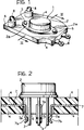
- the present invention relates to an electronic device including an integrated circuit carried by an insulating base, for example, a circuit for regulating the voltage supplied by a motor-vehicle alternator in operation.
- the invention is directed towards an electronic device which includes an integrated circuit encapsulated in a casing and having a plurality of electrical pin terminals which extend from one face of the casing, the integrated circuit being mounted on a support plate or base of electrically insulating material carrying conductive connecting members which are connected to the terminals of the circuit.
- the free ends of the conductive members extend in the hole in the support plate or base outwardly of the corresponding terminals of the integrated circuit and are bent in a manner such that when the integrated circuit is mounted on the plate or base, the terminals of the circuit fit with interference between the ends of the conductive members.
- each conductive member forms a loop which, when the integrated circuit is in the mounted condition, faces and is in contact with the associated terminal of the integrated circuit.
- the free ends of the conductive members are soldered to the associated terminals of the integrated circuit in correspondence with their respective loops.
- an electronic device includes an integrated circuit 1, for example, a voltage-regulator circuit for a motor-vehicle alternator, encapsulated in a casing 2 and having a plurality of metal pin terminals 3 which extend from one face of the casing.
- the casing of the integrated circuit is of a standard type known by the reference TO3 and has two flanges 2a which are fixed to a plate or base 4 of electrically insulating material, for example, by metal rivets 5.
- the support plate or base 4 is moulded from a plastics material and has a hole 6 ( Figure 2) in the region in which the integrated circuit 1 is mounted.
- Conductive connecting members are incorporated in the plate or base 4 at the moulding stage.
- the conductive members have first ends which project from the plate or base 4 to form connecting terminals, indicated 8 in Figure 1, which in general may be of many different shapes.
- the conductive members 7 embedded in the support plate or base 4 have further ends, indicated 7a in Figure 2, in the hole 6 in relative positions substantially corresponding to those of the terminals 3 of the integrated circuit 1.
- the ends 7a of all the conductive members are bent in the same direction, towards the face of the plate or base 4 opposite that bearing the integrated circuit. In particular, these ends are bent in a manner such that when the integrated circuit 1 is mounted on the plate 4, the terminals 3 of the circuit fit with resilient interference between the ends 7a of the conductive members 7.
- each conductive member 7 forms a loop, indicated 7b in Figure 2, which, when the integrated circuit 1 is in the mounted condition, faces and is in contact with an associated terminal 3 of the integrated circuit.
- the ends 7a of the conductive members 7 are then preferably soldered (for example, by electrical soldering) to the terminals 3 of the integrated circuit in correspondence with the loops 7b.
- the invention enables an integrated circuit to be mounted quickly and easily on a support plate or base in a particularly reliable and secure manner.
Landscapes
- Engineering & Computer Science (AREA)
- Microelectronics & Electronic Packaging (AREA)
- Metallurgy (AREA)
- Manufacturing & Machinery (AREA)
- Structures For Mounting Electric Components On Printed Circuit Boards (AREA)
- Coupling Device And Connection With Printed Circuit (AREA)
- Insulated Metal Substrates For Printed Circuits (AREA)
- Structures Or Materials For Encapsulating Or Coating Semiconductor Devices Or Solid State Devices (AREA)
Applications Claiming Priority (2)
| Application Number | Priority Date | Filing Date | Title |
|---|---|---|---|
| IT5334890U | 1990-10-30 | ||
| IT5334890U IT220657Z2 (it) | 1990-10-30 | 1990-10-30 | Dispositivo elettronico comprendente un circuito integrato montato su una basetta isolante. |
Publications (3)
| Publication Number | Publication Date |
|---|---|
| EP0484286A2 true EP0484286A2 (fr) | 1992-05-06 |
| EP0484286A3 EP0484286A3 (en) | 1992-09-30 |
| EP0484286B1 EP0484286B1 (fr) | 1995-10-11 |
Family
ID=11282020
Family Applications (1)
| Application Number | Title | Priority Date | Filing Date |
|---|---|---|---|
| EP19910830446 Expired - Lifetime EP0484286B1 (fr) | 1990-10-30 | 1991-10-22 | Dispositif électronique comprenant un circuit intégré monté sur une base isolante |
Country Status (4)
| Country | Link |
|---|---|
| EP (1) | EP0484286B1 (fr) |
| DE (1) | DE69113741T2 (fr) |
| ES (1) | ES2078498T3 (fr) |
| IT (1) | IT220657Z2 (fr) |
Cited By (2)
| Publication number | Priority date | Publication date | Assignee | Title |
|---|---|---|---|---|
| WO2008116709A1 (fr) * | 2007-03-26 | 2008-10-02 | Robert Bosch Gmbh | Ensemble électrique comprenant au moins une broche de contact électrique et un ensemble de barres conductrices en contact avec ladite broche |
| WO2017001113A1 (fr) * | 2015-06-30 | 2017-01-05 | Osram Gmbh | Support de circuit pour un circuit électronique et procédé de fabrication d'un tel support de circuit |
Family Cites Families (3)
| Publication number | Priority date | Publication date | Assignee | Title |
|---|---|---|---|---|
| US4226492A (en) * | 1979-07-30 | 1980-10-07 | Bell Telephone Laboratories, Incorporated | Electrical interconnection apparatus |
| US4677526A (en) * | 1984-03-01 | 1987-06-30 | Augat Inc. | Plastic pin grid array chip carrier |
| AU1298988A (en) * | 1987-02-19 | 1988-09-14 | Olin Corporation | Process for manufacturing plastic pin grid arrays and the product produced thereby |
-
1990
- 1990-10-30 IT IT5334890U patent/IT220657Z2/it active IP Right Grant
-
1991
- 1991-10-22 EP EP19910830446 patent/EP0484286B1/fr not_active Expired - Lifetime
- 1991-10-22 ES ES91830446T patent/ES2078498T3/es not_active Expired - Lifetime
- 1991-10-22 DE DE1991613741 patent/DE69113741T2/de not_active Expired - Fee Related
Cited By (2)
| Publication number | Priority date | Publication date | Assignee | Title |
|---|---|---|---|---|
| WO2008116709A1 (fr) * | 2007-03-26 | 2008-10-02 | Robert Bosch Gmbh | Ensemble électrique comprenant au moins une broche de contact électrique et un ensemble de barres conductrices en contact avec ladite broche |
| WO2017001113A1 (fr) * | 2015-06-30 | 2017-01-05 | Osram Gmbh | Support de circuit pour un circuit électronique et procédé de fabrication d'un tel support de circuit |
Also Published As
| Publication number | Publication date |
|---|---|
| EP0484286A3 (en) | 1992-09-30 |
| EP0484286B1 (fr) | 1995-10-11 |
| DE69113741D1 (de) | 1995-11-16 |
| DE69113741T2 (de) | 1996-03-21 |
| IT220657Z2 (it) | 1993-10-08 |
| IT9053348V0 (it) | 1990-10-30 |
| IT9053348U1 (it) | 1992-04-30 |
| ES2078498T3 (es) | 1995-12-16 |
Similar Documents
| Publication | Publication Date | Title |
|---|---|---|
| US4973257A (en) | Battery terminal | |
| US5446626A (en) | Pluggable assembly, particularly a relay module for motor vehicles | |
| US4600971A (en) | Lead frames with dielectric housings molded thereon | |
| US5613860A (en) | Universal grounding clip for card-receiving connector | |
| EP0539094B1 (fr) | Moteur électrique miniature | |
| US6413117B1 (en) | Axisymmetric vibrator, vibrator connection, and mounting system | |
| US5035629A (en) | Electrical connector | |
| KR920007273A (ko) | 전기 접속기 및 그 단자 | |
| US4471408A (en) | Piggyback code switch device | |
| US4800358A (en) | Fuse | |
| JP2001054223A (ja) | ヒューズ装置 | |
| US5542853A (en) | Shunted electrical connector | |
| US5709573A (en) | Connector for high density electronic assemblies | |
| US5181852A (en) | Programmable input-output electrical connector | |
| US5343365A (en) | PCB relay having an improved terminal structure | |
| US5238429A (en) | Electrical assembly and connector therefor | |
| EP0907198B1 (fr) | Structure et procédé de connexion d'un composant électrique à un relais électromagnétique | |
| US4883428A (en) | Test socket incorporating circuit elements | |
| EP0484286B1 (fr) | Dispositif électronique comprenant un circuit intégré monté sur une base isolante | |
| US4495257A (en) | Horizontal battery holder for cylinder cells | |
| US6312264B1 (en) | Connecting device | |
| US5195912A (en) | Electrical connectors | |
| US6109932A (en) | Three-dimensional electrical interconnection system | |
| US5629504A (en) | Voltage switch | |
| EP0762559A3 (fr) | Borne de connexion électrique ayant l'extrémité de connexion à souder arrondi |
Legal Events
| Date | Code | Title | Description |
|---|---|---|---|
| PUAI | Public reference made under article 153(3) epc to a published international application that has entered the european phase |
Free format text: ORIGINAL CODE: 0009012 |
|
| AK | Designated contracting states |
Kind code of ref document: A2 Designated state(s): DE ES FR GB SE |
|
| PUAL | Search report despatched |
Free format text: ORIGINAL CODE: 0009013 |
|
| AK | Designated contracting states |
Kind code of ref document: A3 Designated state(s): DE ES FR GB SE |
|
| 17P | Request for examination filed |
Effective date: 19921031 |
|
| 17Q | First examination report despatched |
Effective date: 19941021 |
|
| RAP1 | Party data changed (applicant data changed or rights of an application transferred) |
Owner name: MAGNETI MARELLI S.P.A. |
|
| GRAA | (expected) grant |
Free format text: ORIGINAL CODE: 0009210 |
|
| AK | Designated contracting states |
Kind code of ref document: B1 Designated state(s): DE ES FR GB SE |
|
| REF | Corresponds to: |
Ref document number: 69113741 Country of ref document: DE Date of ref document: 19951116 |
|
| REG | Reference to a national code |
Ref country code: ES Ref legal event code: FG2A Ref document number: 2078498 Country of ref document: ES Kind code of ref document: T3 |
|
| ET | Fr: translation filed | ||
| PLBE | No opposition filed within time limit |
Free format text: ORIGINAL CODE: 0009261 |
|
| STAA | Information on the status of an ep patent application or granted ep patent |
Free format text: STATUS: NO OPPOSITION FILED WITHIN TIME LIMIT |
|
| 26N | No opposition filed | ||
| REG | Reference to a national code |
Ref country code: GB Ref legal event code: IF02 |
|
| PGFP | Annual fee paid to national office [announced via postgrant information from national office to epo] |
Ref country code: ES Payment date: 20060904 Year of fee payment: 16 |
|
| PGFP | Annual fee paid to national office [announced via postgrant information from national office to epo] |
Ref country code: GB Payment date: 20060914 Year of fee payment: 16 |
|
| PGFP | Annual fee paid to national office [announced via postgrant information from national office to epo] |
Ref country code: DE Payment date: 20060925 Year of fee payment: 16 |
|
| PGFP | Annual fee paid to national office [announced via postgrant information from national office to epo] |
Ref country code: FR Payment date: 20061031 Year of fee payment: 16 |
|
| PGFP | Annual fee paid to national office [announced via postgrant information from national office to epo] |
Ref country code: SE Payment date: 20060831 Year of fee payment: 16 |
|
| EUG | Se: european patent has lapsed | ||
| GBPC | Gb: european patent ceased through non-payment of renewal fee |
Effective date: 20071022 |
|
| PG25 | Lapsed in a contracting state [announced via postgrant information from national office to epo] |
Ref country code: DE Free format text: LAPSE BECAUSE OF NON-PAYMENT OF DUE FEES Effective date: 20080501 |
|
| REG | Reference to a national code |
Ref country code: FR Ref legal event code: ST Effective date: 20080630 |
|
| PG25 | Lapsed in a contracting state [announced via postgrant information from national office to epo] |
Ref country code: SE Free format text: LAPSE BECAUSE OF NON-PAYMENT OF DUE FEES Effective date: 20071023 |
|
| PG25 | Lapsed in a contracting state [announced via postgrant information from national office to epo] |
Ref country code: GB Free format text: LAPSE BECAUSE OF NON-PAYMENT OF DUE FEES Effective date: 20071022 |
|
| REG | Reference to a national code |
Ref country code: ES Ref legal event code: FD2A Effective date: 20071023 |
|
| PG25 | Lapsed in a contracting state [announced via postgrant information from national office to epo] |
Ref country code: FR Free format text: LAPSE BECAUSE OF NON-PAYMENT OF DUE FEES Effective date: 20071031 Ref country code: ES Free format text: LAPSE BECAUSE OF NON-PAYMENT OF DUE FEES Effective date: 20071023 |