EP0484286A2 - An electronic device including an integrated circuit mounted on an insulating base - Google Patents
An electronic device including an integrated circuit mounted on an insulating base Download PDFInfo
- Publication number
- EP0484286A2 EP0484286A2 EP91830446A EP91830446A EP0484286A2 EP 0484286 A2 EP0484286 A2 EP 0484286A2 EP 91830446 A EP91830446 A EP 91830446A EP 91830446 A EP91830446 A EP 91830446A EP 0484286 A2 EP0484286 A2 EP 0484286A2
- Authority
- EP
- European Patent Office
- Prior art keywords
- integrated circuit
- terminals
- base
- plate
- conductive
- Prior art date
- Legal status (The legal status is an assumption and is not a legal conclusion. Google has not performed a legal analysis and makes no representation as to the accuracy of the status listed.)
- Granted
Links
Images
Classifications
-
- H—ELECTRICITY
- H05—ELECTRIC TECHNIQUES NOT OTHERWISE PROVIDED FOR
- H05K—PRINTED CIRCUITS; CASINGS OR CONSTRUCTIONAL DETAILS OF ELECTRIC APPARATUS; MANUFACTURE OF ASSEMBLAGES OF ELECTRICAL COMPONENTS
- H05K3/00—Apparatus or processes for manufacturing printed circuits
- H05K3/30—Assembling printed circuits with electric components, e.g. with resistors
- H05K3/32—Assembling printed circuits with electric components, e.g. with resistors electrically connecting electric components or wires to printed circuits
- H05K3/325—Assembling printed circuits with electric components, e.g. with resistors electrically connecting electric components or wires to printed circuits by abutting or pinching; Mechanical auxiliary parts therefor
- H05K3/326—Assembling printed circuits with electric components, e.g. with resistors electrically connecting electric components or wires to printed circuits by abutting or pinching; Mechanical auxiliary parts therefor the printed circuit having integral resilient or deformable parts, e.g. tabs or parts of flexible circuits
-
- H—ELECTRICITY
- H05—ELECTRIC TECHNIQUES NOT OTHERWISE PROVIDED FOR
- H05K—PRINTED CIRCUITS; CASINGS OR CONSTRUCTIONAL DETAILS OF ELECTRIC APPARATUS; MANUFACTURE OF ASSEMBLAGES OF ELECTRICAL COMPONENTS
- H05K7/00—Constructional details common to different types of electric apparatus
- H05K7/02—Arrangements of circuit components or wiring on supporting structure
- H05K7/10—Plug-in assemblages of components, e.g. IC sockets
- H05K7/1053—Plug-in assemblages of components, e.g. IC sockets having interior leads
- H05K7/1061—Plug-in assemblages of components, e.g. IC sockets having interior leads co-operating by abutting
- H05K7/1069—Plug-in assemblages of components, e.g. IC sockets having interior leads co-operating by abutting with spring contact pieces
-
- H—ELECTRICITY
- H05—ELECTRIC TECHNIQUES NOT OTHERWISE PROVIDED FOR
- H05K—PRINTED CIRCUITS; CASINGS OR CONSTRUCTIONAL DETAILS OF ELECTRIC APPARATUS; MANUFACTURE OF ASSEMBLAGES OF ELECTRICAL COMPONENTS
- H05K2201/00—Indexing scheme relating to printed circuits covered by H05K1/00
- H05K2201/03—Conductive materials
- H05K2201/0332—Structure of the conductor
- H05K2201/0388—Other aspects of conductors
- H05K2201/0397—Tab
-
- H—ELECTRICITY
- H05—ELECTRIC TECHNIQUES NOT OTHERWISE PROVIDED FOR
- H05K—PRINTED CIRCUITS; CASINGS OR CONSTRUCTIONAL DETAILS OF ELECTRIC APPARATUS; MANUFACTURE OF ASSEMBLAGES OF ELECTRICAL COMPONENTS
- H05K2201/00—Indexing scheme relating to printed circuits covered by H05K1/00
- H05K2201/09—Shape and layout
- H05K2201/09009—Substrate related
- H05K2201/09118—Moulded substrate
-
- H—ELECTRICITY
- H05—ELECTRIC TECHNIQUES NOT OTHERWISE PROVIDED FOR
- H05K—PRINTED CIRCUITS; CASINGS OR CONSTRUCTIONAL DETAILS OF ELECTRIC APPARATUS; MANUFACTURE OF ASSEMBLAGES OF ELECTRICAL COMPONENTS
- H05K2201/00—Indexing scheme relating to printed circuits covered by H05K1/00
- H05K2201/10—Details of components or other objects attached to or integrated in a printed circuit board
- H05K2201/10431—Details of mounted components
- H05K2201/1059—Connections made by press-fit insertion
-
- H—ELECTRICITY
- H05—ELECTRIC TECHNIQUES NOT OTHERWISE PROVIDED FOR
- H05K—PRINTED CIRCUITS; CASINGS OR CONSTRUCTIONAL DETAILS OF ELECTRIC APPARATUS; MANUFACTURE OF ASSEMBLAGES OF ELECTRICAL COMPONENTS
- H05K2201/00—Indexing scheme relating to printed circuits covered by H05K1/00
- H05K2201/10—Details of components or other objects attached to or integrated in a printed circuit board
- H05K2201/10613—Details of electrical connections of non-printed components, e.g. special leads
- H05K2201/10621—Components characterised by their electrical contacts
- H05K2201/10689—Leaded Integrated Circuit [IC] package, e.g. dual-in-line [DIL]
-
- H—ELECTRICITY
- H05—ELECTRIC TECHNIQUES NOT OTHERWISE PROVIDED FOR
- H05K—PRINTED CIRCUITS; CASINGS OR CONSTRUCTIONAL DETAILS OF ELECTRIC APPARATUS; MANUFACTURE OF ASSEMBLAGES OF ELECTRICAL COMPONENTS
- H05K3/00—Apparatus or processes for manufacturing printed circuits
- H05K3/10—Apparatus or processes for manufacturing printed circuits in which conductive material is applied to the insulating support in such a manner as to form the desired conductive pattern
- H05K3/20—Apparatus or processes for manufacturing printed circuits in which conductive material is applied to the insulating support in such a manner as to form the desired conductive pattern by affixing prefabricated conductor pattern
- H05K3/202—Apparatus or processes for manufacturing printed circuits in which conductive material is applied to the insulating support in such a manner as to form the desired conductive pattern by affixing prefabricated conductor pattern using self-supporting metal foil pattern
-
- H—ELECTRICITY
- H05—ELECTRIC TECHNIQUES NOT OTHERWISE PROVIDED FOR
- H05K—PRINTED CIRCUITS; CASINGS OR CONSTRUCTIONAL DETAILS OF ELECTRIC APPARATUS; MANUFACTURE OF ASSEMBLAGES OF ELECTRICAL COMPONENTS
- H05K3/00—Apparatus or processes for manufacturing printed circuits
- H05K3/30—Assembling printed circuits with electric components, e.g. with resistors
- H05K3/306—Assembling printed circuits with electric components, e.g. with resistors with lead-in-hole components
-
- H—ELECTRICITY
- H05—ELECTRIC TECHNIQUES NOT OTHERWISE PROVIDED FOR
- H05K—PRINTED CIRCUITS; CASINGS OR CONSTRUCTIONAL DETAILS OF ELECTRIC APPARATUS; MANUFACTURE OF ASSEMBLAGES OF ELECTRICAL COMPONENTS
- H05K3/00—Apparatus or processes for manufacturing printed circuits
- H05K3/40—Forming printed elements for providing electric connections to or between printed circuits
- H05K3/4092—Integral conductive tabs, i.e. conductive parts partly detached from the substrate
Definitions
- the present invention relates to an electronic device including an integrated circuit carried by an insulating base, for example, a circuit for regulating the voltage supplied by a motor-vehicle alternator in operation.
- the invention is directed towards an electronic device which includes an integrated circuit encapsulated in a casing and having a plurality of electrical pin terminals which extend from one face of the casing, the integrated circuit being mounted on a support plate or base of electrically insulating material carrying conductive connecting members which are connected to the terminals of the circuit.
- the free ends of the conductive members extend in the hole in the support plate or base outwardly of the corresponding terminals of the integrated circuit and are bent in a manner such that when the integrated circuit is mounted on the plate or base, the terminals of the circuit fit with interference between the ends of the conductive members.
- each conductive member forms a loop which, when the integrated circuit is in the mounted condition, faces and is in contact with the associated terminal of the integrated circuit.
- the free ends of the conductive members are soldered to the associated terminals of the integrated circuit in correspondence with their respective loops.
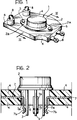
- an electronic device includes an integrated circuit 1, for example, a voltage-regulator circuit for a motor-vehicle alternator, encapsulated in a casing 2 and having a plurality of metal pin terminals 3 which extend from one face of the casing.
- the casing of the integrated circuit is of a standard type known by the reference TO3 and has two flanges 2a which are fixed to a plate or base 4 of electrically insulating material, for example, by metal rivets 5.
- the support plate or base 4 is moulded from a plastics material and has a hole 6 ( Figure 2) in the region in which the integrated circuit 1 is mounted.
- Conductive connecting members are incorporated in the plate or base 4 at the moulding stage.
- the conductive members have first ends which project from the plate or base 4 to form connecting terminals, indicated 8 in Figure 1, which in general may be of many different shapes.
- the conductive members 7 embedded in the support plate or base 4 have further ends, indicated 7a in Figure 2, in the hole 6 in relative positions substantially corresponding to those of the terminals 3 of the integrated circuit 1.
- the ends 7a of all the conductive members are bent in the same direction, towards the face of the plate or base 4 opposite that bearing the integrated circuit. In particular, these ends are bent in a manner such that when the integrated circuit 1 is mounted on the plate 4, the terminals 3 of the circuit fit with resilient interference between the ends 7a of the conductive members 7.
- each conductive member 7 forms a loop, indicated 7b in Figure 2, which, when the integrated circuit 1 is in the mounted condition, faces and is in contact with an associated terminal 3 of the integrated circuit.
- the ends 7a of the conductive members 7 are then preferably soldered (for example, by electrical soldering) to the terminals 3 of the integrated circuit in correspondence with the loops 7b.
- the invention enables an integrated circuit to be mounted quickly and easily on a support plate or base in a particularly reliable and secure manner.
Landscapes
- Engineering & Computer Science (AREA)
- Microelectronics & Electronic Packaging (AREA)
- Metallurgy (AREA)
- Manufacturing & Machinery (AREA)
- Insulated Metal Substrates For Printed Circuits (AREA)
- Coupling Device And Connection With Printed Circuit (AREA)
- Structures Or Materials For Encapsulating Or Coating Semiconductor Devices Or Solid State Devices (AREA)
- Structures For Mounting Electric Components On Printed Circuit Boards (AREA)
Abstract
Description
- The present invention relates to an electronic device including an integrated circuit carried by an insulating base, for example, a circuit for regulating the voltage supplied by a motor-vehicle alternator in operation.
- More specifically, the invention is directed towards an electronic device which includes an integrated circuit encapsulated in a casing and having a plurality of electrical pin terminals which extend from one face of the casing, the integrated circuit being mounted on a support plate or base of electrically insulating material carrying conductive connecting members which are connected to the terminals of the circuit.
- The device according to the invention is characterised in that:
- the support plate or base is moulded from a plastics material and has a hole in the region in which the integrated circuit is mounted,
- the conductive connecting members are at least partially embedded in the plate or base and have respective free ends in the hole in relative positions substantially corresponding to those of the terminals of the integrated circuit, the free ends of all the conductive members being bent in the same direction towards the face of the plate or base opposite that bearing the integrated circuit so as to be at least partially in contact with the corresponding terminals of the integrated circuit.
- According to a further characteristic, conveniently, the free ends of the conductive members extend in the hole in the support plate or base outwardly of the corresponding terminals of the integrated circuit and are bent in a manner such that when the integrated circuit is mounted on the plate or base, the terminals of the circuit fit with interference between the ends of the conductive members.
- To advantage, the end portion of the free end of each conductive member forms a loop which, when the integrated circuit is in the mounted condition, faces and is in contact with the associated terminal of the integrated circuit.
- Preferably, the free ends of the conductive members are soldered to the associated terminals of the integrated circuit in correspondence with their respective loops.
- Further characteristics and advantages of the invention will become clear from the detailed description which follows with reference to the appended drawings, provided purely by way of non-limiting example, in which:
- Figure 1 is a perspective view of a device according to the invention, and
- Figure 2 is a partial sectional view taken on the line II-II of Figure 1, on an enlarged scale.
- With reference to Figure 1, an electronic device according to the invention includes an integrated circuit 1, for example, a voltage-regulator circuit for a motor-vehicle alternator, encapsulated in a
casing 2 and having a plurality of metal pin terminals 3 which extend from one face of the casing. In the embodiment shown by way of example, the casing of the integrated circuit is of a standard type known by the reference TO3 and has twoflanges 2a which are fixed to a plate orbase 4 of electrically insulating material, for example, bymetal rivets 5. - Conveniently, the support plate or
base 4 is moulded from a plastics material and has a hole 6 (Figure 2) in the region in which the integrated circuit 1 is mounted. - Conductive connecting members, indicated 7, of which three are partly visible in Figure 2, are incorporated in the plate or
base 4 at the moulding stage. The conductive members have first ends which project from the plate orbase 4 to form connecting terminals, indicated 8 in Figure 1, which in general may be of many different shapes. - The
conductive members 7 embedded in the support plate orbase 4 have further ends, indicated 7a in Figure 2, in the hole 6 in relative positions substantially corresponding to those of the terminals 3 of the integrated circuit 1. Theends 7a of all the conductive members are bent in the same direction, towards the face of the plate orbase 4 opposite that bearing the integrated circuit. In particular, these ends are bent in a manner such that when the integrated circuit 1 is mounted on theplate 4, the terminals 3 of the circuit fit with resilient interference between theends 7a of theconductive members 7. - Conveniently, the end portion of the
end 7a of eachconductive member 7 forms a loop, indicated 7b in Figure 2, which, when the integrated circuit 1 is in the mounted condition, faces and is in contact with an associated terminal 3 of the integrated circuit. Theends 7a of theconductive members 7 are then preferably soldered (for example, by electrical soldering) to the terminals 3 of the integrated circuit in correspondence with theloops 7b. - The invention enables an integrated circuit to be mounted quickly and easily on a support plate or base in a particularly reliable and secure manner.
Claims (4)
- An electronic device including an integrated circuit (1) encapsulated in a casing (2) and having a plurality of metal pin terminals (3) which extend from one face of the casing (2), the integrated circuit (1) being mounted on a support plate or base (4) of electrically insulating material carrying conductive connecting members (7) which are connected to the terminals (3) of the circuit (1),
characterised in that:- the support plate or base (4) is moulded from a plastics material and has a hole (6) in the region in which the integrated circuit (1) is mounted,- the conductive connecting members (7) are at least partially embedded in the plate or base (4) and have respective free ends (7a) in the hole (6) in relative positions substantially corresponding to those of the terminals (3) of the integrated circuit (1), the free ends (7a) of all the conductive members (7) being bent in the same direction towards the face of the plate or base (4) opposite that bearing the integrated circuit (1) so as to be at least partially in contact with the corresponding terminals (3) of the integrated circuit (1). - A device according to Claim 1, characterised in that the free ends (7a) of the conductive members (7) extend in the hole (6) outwardly of the corresponding terminals (3) of the integrated circuit (1) and are bent in a manner such that when the integrated circuit (1) is mounted on the support plate or base (4), the terminals (3) of the integrated circuit (1) fit with interference between the ends (7a) of the conductive members (7).
- A device according to Claim 2, characterised in that the end portion of the free end (7a) of each conductive member (7) forms a loop (7b) which, when the integrated circuit (1) is in the mounted condition, faces and is in contact with an associated terminal (3) of the integrated circuit (1).
- A device according to Claim 3, charcterised in that the free ends (7a) of the conductive members (7) are soldered to the associated terminals (3) of the integrated circuit (1) in correspondence with their respective loops (7b).
Applications Claiming Priority (2)
| Application Number | Priority Date | Filing Date | Title |
|---|---|---|---|
| IT5334890U IT220657Z2 (en) | 1990-10-30 | 1990-10-30 | ELECTRONIC DEVICE INCLUDING AN INTEGRATED CIRCUIT MOUNTED ON AN INSULATING BASE. |
| IT5334890U | 1990-10-30 |
Publications (3)
| Publication Number | Publication Date |
|---|---|
| EP0484286A2 true EP0484286A2 (en) | 1992-05-06 |
| EP0484286A3 EP0484286A3 (en) | 1992-09-30 |
| EP0484286B1 EP0484286B1 (en) | 1995-10-11 |
Family
ID=11282020
Family Applications (1)
| Application Number | Title | Priority Date | Filing Date |
|---|---|---|---|
| EP19910830446 Expired - Lifetime EP0484286B1 (en) | 1990-10-30 | 1991-10-22 | An electronic device including an integrated circuit mounted on an insulating base |
Country Status (4)
| Country | Link |
|---|---|
| EP (1) | EP0484286B1 (en) |
| DE (1) | DE69113741T2 (en) |
| ES (1) | ES2078498T3 (en) |
| IT (1) | IT220657Z2 (en) |
Cited By (2)
| Publication number | Priority date | Publication date | Assignee | Title |
|---|---|---|---|---|
| WO2008116709A1 (en) * | 2007-03-26 | 2008-10-02 | Robert Bosch Gmbh | Electrical arrangement comprising at least one electrical contact pin and a conductor rail arrangement contacted thereby |
| WO2017001113A1 (en) * | 2015-06-30 | 2017-01-05 | Osram Gmbh | Circuit support for an electronic circuit, and method for manufacturing a circuit support of said type |
Family Cites Families (3)
| Publication number | Priority date | Publication date | Assignee | Title |
|---|---|---|---|---|
| US4226492A (en) * | 1979-07-30 | 1980-10-07 | Bell Telephone Laboratories, Incorporated | Electrical interconnection apparatus |
| US4677526A (en) * | 1984-03-01 | 1987-06-30 | Augat Inc. | Plastic pin grid array chip carrier |
| KR960010011B1 (en) * | 1987-02-19 | 1996-07-25 | 폴 와인스타인 | Process for manufacturing plastic pin grid arrays and the product produced thereby |
-
1990
- 1990-10-30 IT IT5334890U patent/IT220657Z2/en active IP Right Grant
-
1991
- 1991-10-22 DE DE1991613741 patent/DE69113741T2/en not_active Expired - Fee Related
- 1991-10-22 EP EP19910830446 patent/EP0484286B1/en not_active Expired - Lifetime
- 1991-10-22 ES ES91830446T patent/ES2078498T3/en not_active Expired - Lifetime
Cited By (2)
| Publication number | Priority date | Publication date | Assignee | Title |
|---|---|---|---|---|
| WO2008116709A1 (en) * | 2007-03-26 | 2008-10-02 | Robert Bosch Gmbh | Electrical arrangement comprising at least one electrical contact pin and a conductor rail arrangement contacted thereby |
| WO2017001113A1 (en) * | 2015-06-30 | 2017-01-05 | Osram Gmbh | Circuit support for an electronic circuit, and method for manufacturing a circuit support of said type |
Also Published As
| Publication number | Publication date |
|---|---|
| ES2078498T3 (en) | 1995-12-16 |
| IT9053348V0 (en) | 1990-10-30 |
| IT220657Z2 (en) | 1993-10-08 |
| IT9053348U1 (en) | 1992-04-30 |
| EP0484286A3 (en) | 1992-09-30 |
| DE69113741D1 (en) | 1995-11-16 |
| EP0484286B1 (en) | 1995-10-11 |
| DE69113741T2 (en) | 1996-03-21 |
Similar Documents
| Publication | Publication Date | Title |
|---|---|---|
| US4973257A (en) | Battery terminal | |
| US5446626A (en) | Pluggable assembly, particularly a relay module for motor vehicles | |
| US4600971A (en) | Lead frames with dielectric housings molded thereon | |
| US5613860A (en) | Universal grounding clip for card-receiving connector | |
| EP0539094B1 (en) | A miniature electric motor | |
| US6413117B1 (en) | Axisymmetric vibrator, vibrator connection, and mounting system | |
| US5035629A (en) | Electrical connector | |
| KR920007273A (en) | Electrical connector and its terminals | |
| US4471408A (en) | Piggyback code switch device | |
| US4800358A (en) | Fuse | |
| US5542853A (en) | Shunted electrical connector | |
| US5709573A (en) | Connector for high density electronic assemblies | |
| US5181852A (en) | Programmable input-output electrical connector | |
| US5343365A (en) | PCB relay having an improved terminal structure | |
| US5238429A (en) | Electrical assembly and connector therefor | |
| EP0907198B1 (en) | Structure and method for connection of an electrical component to an electromagnetic relay | |
| US4883428A (en) | Test socket incorporating circuit elements | |
| EP0484286B1 (en) | An electronic device including an integrated circuit mounted on an insulating base | |
| US4495257A (en) | Horizontal battery holder for cylinder cells | |
| US6312264B1 (en) | Connecting device | |
| US5195912A (en) | Electrical connectors | |
| US6109932A (en) | Three-dimensional electrical interconnection system | |
| US5629504A (en) | Voltage switch | |
| EP0762559A3 (en) | Electric connector terminal having a round soldering tail | |
| US3076172A (en) | Contact clip |
Legal Events
| Date | Code | Title | Description |
|---|---|---|---|
| PUAI | Public reference made under article 153(3) epc to a published international application that has entered the european phase |
Free format text: ORIGINAL CODE: 0009012 |
|
| AK | Designated contracting states |
Kind code of ref document: A2 Designated state(s): DE ES FR GB SE |
|
| PUAL | Search report despatched |
Free format text: ORIGINAL CODE: 0009013 |
|
| AK | Designated contracting states |
Kind code of ref document: A3 Designated state(s): DE ES FR GB SE |
|
| 17P | Request for examination filed |
Effective date: 19921031 |
|
| 17Q | First examination report despatched |
Effective date: 19941021 |
|
| RAP1 | Party data changed (applicant data changed or rights of an application transferred) |
Owner name: MAGNETI MARELLI S.P.A. |
|
| GRAA | (expected) grant |
Free format text: ORIGINAL CODE: 0009210 |
|
| AK | Designated contracting states |
Kind code of ref document: B1 Designated state(s): DE ES FR GB SE |
|
| REF | Corresponds to: |
Ref document number: 69113741 Country of ref document: DE Date of ref document: 19951116 |
|
| REG | Reference to a national code |
Ref country code: ES Ref legal event code: FG2A Ref document number: 2078498 Country of ref document: ES Kind code of ref document: T3 |
|
| ET | Fr: translation filed | ||
| PLBE | No opposition filed within time limit |
Free format text: ORIGINAL CODE: 0009261 |
|
| STAA | Information on the status of an ep patent application or granted ep patent |
Free format text: STATUS: NO OPPOSITION FILED WITHIN TIME LIMIT |
|
| 26N | No opposition filed | ||
| REG | Reference to a national code |
Ref country code: GB Ref legal event code: IF02 |
|
| PGFP | Annual fee paid to national office [announced via postgrant information from national office to epo] |
Ref country code: ES Payment date: 20060904 Year of fee payment: 16 |
|
| PGFP | Annual fee paid to national office [announced via postgrant information from national office to epo] |
Ref country code: GB Payment date: 20060914 Year of fee payment: 16 |
|
| PGFP | Annual fee paid to national office [announced via postgrant information from national office to epo] |
Ref country code: DE Payment date: 20060925 Year of fee payment: 16 |
|
| PGFP | Annual fee paid to national office [announced via postgrant information from national office to epo] |
Ref country code: FR Payment date: 20061031 Year of fee payment: 16 |
|
| PGFP | Annual fee paid to national office [announced via postgrant information from national office to epo] |
Ref country code: SE Payment date: 20060831 Year of fee payment: 16 |
|
| EUG | Se: european patent has lapsed | ||
| GBPC | Gb: european patent ceased through non-payment of renewal fee |
Effective date: 20071022 |
|
| PG25 | Lapsed in a contracting state [announced via postgrant information from national office to epo] |
Ref country code: DE Free format text: LAPSE BECAUSE OF NON-PAYMENT OF DUE FEES Effective date: 20080501 |
|
| REG | Reference to a national code |
Ref country code: FR Ref legal event code: ST Effective date: 20080630 |
|
| PG25 | Lapsed in a contracting state [announced via postgrant information from national office to epo] |
Ref country code: SE Free format text: LAPSE BECAUSE OF NON-PAYMENT OF DUE FEES Effective date: 20071023 |
|
| PG25 | Lapsed in a contracting state [announced via postgrant information from national office to epo] |
Ref country code: GB Free format text: LAPSE BECAUSE OF NON-PAYMENT OF DUE FEES Effective date: 20071022 |
|
| REG | Reference to a national code |
Ref country code: ES Ref legal event code: FD2A Effective date: 20071023 |
|
| PG25 | Lapsed in a contracting state [announced via postgrant information from national office to epo] |
Ref country code: FR Free format text: LAPSE BECAUSE OF NON-PAYMENT OF DUE FEES Effective date: 20071031 Ref country code: ES Free format text: LAPSE BECAUSE OF NON-PAYMENT OF DUE FEES Effective date: 20071023 |