EP0484164B1 - A row electrode driving circuit for a display apparatus - Google Patents
A row electrode driving circuit for a display apparatus Download PDFInfo
- Publication number
- EP0484164B1 EP0484164B1 EP91310092A EP91310092A EP0484164B1 EP 0484164 B1 EP0484164 B1 EP 0484164B1 EP 91310092 A EP91310092 A EP 91310092A EP 91310092 A EP91310092 A EP 91310092A EP 0484164 B1 EP0484164 B1 EP 0484164B1
- Authority
- EP
- European Patent Office
- Prior art keywords
- electrode driving
- row electrode
- driving circuit
- signal
- circuit
- Prior art date
- Legal status (The legal status is an assumption and is not a legal conclusion. Google has not performed a legal analysis and makes no representation as to the accuracy of the status listed.)
- Expired - Lifetime
Links
- 239000004973 liquid crystal related substance Substances 0.000 claims description 3
- 238000010586 diagram Methods 0.000 description 4
- 239000011159 matrix material Substances 0.000 description 4
- 101150046174 NIP2-1 gene Proteins 0.000 description 2
- 101100075512 Oryza sativa subsp. japonica LSI2 gene Proteins 0.000 description 2
- 101100075513 Oryza sativa subsp. japonica LSI3 gene Proteins 0.000 description 2
- 230000000694 effects Effects 0.000 description 2
- 230000001419 dependent effect Effects 0.000 description 1
- 238000005070 sampling Methods 0.000 description 1
- 239000000758 substrate Substances 0.000 description 1
- 230000001360 synchronised effect Effects 0.000 description 1
- 239000010409 thin film Substances 0.000 description 1
Images


Classifications
-
- G—PHYSICS
- G09—EDUCATION; CRYPTOGRAPHY; DISPLAY; ADVERTISING; SEALS
- G09G—ARRANGEMENTS OR CIRCUITS FOR CONTROL OF INDICATING DEVICES USING STATIC MEANS TO PRESENT VARIABLE INFORMATION
- G09G3/00—Control arrangements or circuits, of interest only in connection with visual indicators other than cathode-ray tubes
- G09G3/20—Control arrangements or circuits, of interest only in connection with visual indicators other than cathode-ray tubes for presentation of an assembly of a number of characters, e.g. a page, by composing the assembly by combination of individual elements arranged in a matrix no fixed position being assigned to or needed to be assigned to the individual characters or partial characters
- G09G3/34—Control arrangements or circuits, of interest only in connection with visual indicators other than cathode-ray tubes for presentation of an assembly of a number of characters, e.g. a page, by composing the assembly by combination of individual elements arranged in a matrix no fixed position being assigned to or needed to be assigned to the individual characters or partial characters by control of light from an independent source
- G09G3/36—Control arrangements or circuits, of interest only in connection with visual indicators other than cathode-ray tubes for presentation of an assembly of a number of characters, e.g. a page, by composing the assembly by combination of individual elements arranged in a matrix no fixed position being assigned to or needed to be assigned to the individual characters or partial characters by control of light from an independent source using liquid crystals
- G09G3/3611—Control of matrices with row and column drivers
- G09G3/3674—Details of drivers for scan electrodes
- G09G3/3677—Details of drivers for scan electrodes suitable for active matrices only
-
- G—PHYSICS
- G09—EDUCATION; CRYPTOGRAPHY; DISPLAY; ADVERTISING; SEALS
- G09G—ARRANGEMENTS OR CIRCUITS FOR CONTROL OF INDICATING DEVICES USING STATIC MEANS TO PRESENT VARIABLE INFORMATION
- G09G2310/00—Command of the display device
- G09G2310/02—Addressing, scanning or driving the display screen or processing steps related thereto
- G09G2310/0264—Details of driving circuits
- G09G2310/0283—Arrangement of drivers for different directions of scanning
Definitions
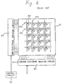
- a matrix type liquid crystal display (LCD) apparatus As a typical example of a matrix type display device, a matrix type liquid crystal display (LCD) apparatus is shown in Figure 6.
- the LCD apparatus of Figure 6 comprises an LCD panel 61 having: a plurality of row electrodes 61a which are disposed on a substrate parallel to one another; and a plurality of column electrodes 61b which intersect the row electrodes 61a .
- a pair of a picture element (pixel) electrode 61c and a thin film transistor (TFT) 61d which functions as a switching element is disposed at each crossing of the row electrodes 61a and the column electrodes 61b .
- the LCD panel 61 is driven by a row electrode driving circuit 62 and column electrode driving circuit 63 .
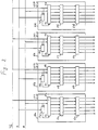
- pulse signals are sequentially output to the lines q 1, q 2, ..., q n from the shift register circuit 71 .
- the voltage signals Q 1, Q 2, ..., Q n converted by level shifter circuit 72 are output through the buffer circuit 73 , based on this pulse signal.
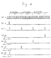
- Figures 3 and 4 are timing charts illustrating the operation of the row electrode driving circuit of Figure 2.
- the shift register control circuit 14 comprises a count circuit 15 , a timing selection circuit 16 , and a switching circuit 17 .
- the count circuit 15 supplies a count signal C to the timing selection circuit 16 immediately after receiving the start signal S , and every time k clock pulses ⁇ (k is the number of steps in the shift register circuit 11 ) are counted after the input of the start signal S .
- the switching circuit 17 supplies externally established data l, when the shift direction control signal U/L is U, and data (n - 1 - l), when the shift direction control signal U/L is L, to the timing selection circuit 16 .
- the invention it is not necessary to produce digital signals between partial row electrode driving circuits. In the row electrode driving circuits of the invention, therefore, image disturbance due to noise resulting from digital signals can be eliminated. Furthermore, in the row electrode driving circuits of the invention, the sequence of driving row electrodes in a display apparatus can be easily reversed by controlling the shift direction control signal.
Landscapes
- Engineering & Computer Science (AREA)
- Chemical & Material Sciences (AREA)
- Crystallography & Structural Chemistry (AREA)
- Physics & Mathematics (AREA)
- Computer Hardware Design (AREA)
- General Physics & Mathematics (AREA)
- Theoretical Computer Science (AREA)
- Liquid Crystal Display Device Control (AREA)
- Control Of Indicators Other Than Cathode Ray Tubes (AREA)
- Liquid Crystal (AREA)
Applications Claiming Priority (2)
| Application Number | Priority Date | Filing Date | Title |
|---|---|---|---|
| JP296164/90 | 1990-10-31 | ||
| JP2296164A JPH04168477A (ja) | 1990-10-31 | 1990-10-31 | 表示装置の行電極駆動回路 |
Publications (3)
| Publication Number | Publication Date |
|---|---|
| EP0484164A2 EP0484164A2 (en) | 1992-05-06 |
| EP0484164A3 EP0484164A3 (en) | 1992-10-28 |
| EP0484164B1 true EP0484164B1 (en) | 1996-01-31 |
Family
ID=17829988
Family Applications (1)
| Application Number | Title | Priority Date | Filing Date |
|---|---|---|---|
| EP91310092A Expired - Lifetime EP0484164B1 (en) | 1990-10-31 | 1991-10-31 | A row electrode driving circuit for a display apparatus |
Country Status (6)
| Country | Link |
|---|---|
| US (1) | US5253093A (enExample) |
| EP (1) | EP0484164B1 (enExample) |
| JP (1) | JPH04168477A (enExample) |
| KR (1) | KR960008102B1 (enExample) |
| DE (1) | DE69116798T2 (enExample) |
| TW (1) | TW211069B (enExample) |
Families Citing this family (6)
| Publication number | Priority date | Publication date | Assignee | Title |
|---|---|---|---|---|
| EP0559321B1 (en) * | 1992-01-31 | 1997-07-09 | Canon Kabushiki Kaisha | Active matrix liquid crystal light valve with driver circuit |
| US5532712A (en) * | 1993-04-13 | 1996-07-02 | Kabushiki Kaisha Komatsu Seisakusho | Drive circuit for use with transmissive scattered liquid crystal display device |
| JP3059048B2 (ja) * | 1994-05-19 | 2000-07-04 | シャープ株式会社 | 液晶表示装置及びその駆動方法 |
| JPH08106272A (ja) * | 1994-10-03 | 1996-04-23 | Semiconductor Energy Lab Co Ltd | 表示装置駆動回路 |
| US7050036B2 (en) | 2001-12-12 | 2006-05-23 | Lg.Philips Lcd Co., Ltd. | Shift register with a built in level shifter |
| TWI413986B (zh) * | 2009-07-01 | 2013-11-01 | Au Optronics Corp | 移位暫存器 |
Family Cites Families (9)
| Publication number | Priority date | Publication date | Assignee | Title |
|---|---|---|---|---|
| JPS54126497A (en) * | 1978-03-24 | 1979-10-01 | Sharp Corp | Dap-type liquid crystal display device |
| JPS58216289A (ja) * | 1982-06-10 | 1983-12-15 | シャープ株式会社 | 液晶表示装置駆動回路 |
| DE3380465D1 (en) * | 1982-09-20 | 1989-09-28 | Toshiba Kk | Video ram write control apparatus |
| JPS6132093A (ja) * | 1984-07-23 | 1986-02-14 | シャープ株式会社 | 液晶表示装置の駆動回路 |
| ES2044845T3 (es) * | 1986-02-17 | 1994-01-16 | Canon Kk | Aparato excitador. |
| JPH061312B2 (ja) * | 1986-02-20 | 1994-01-05 | 富士写真フイルム株式会社 | 液晶駆動制御装置 |
| EP0275140B1 (en) * | 1987-01-09 | 1995-07-19 | Hitachi, Ltd. | Method and circuit for scanning capacitive loads |
| JPH0654421B2 (ja) * | 1987-12-07 | 1994-07-20 | シャープ株式会社 | マトリクス型液晶表示装置の列電極駆動回路 |
| JPH03198087A (ja) * | 1989-12-27 | 1991-08-29 | Sharp Corp | 表示装置の列電極駆動回路 |
-
1990
- 1990-10-31 JP JP2296164A patent/JPH04168477A/ja active Pending
-
1991
- 1991-10-29 US US07/783,890 patent/US5253093A/en not_active Expired - Lifetime
- 1991-10-29 TW TW080108476A patent/TW211069B/zh active
- 1991-10-31 DE DE69116798T patent/DE69116798T2/de not_active Expired - Fee Related
- 1991-10-31 EP EP91310092A patent/EP0484164B1/en not_active Expired - Lifetime
- 1991-11-04 KR KR1019910019503A patent/KR960008102B1/ko not_active Expired - Fee Related
Also Published As
| Publication number | Publication date |
|---|---|
| DE69116798T2 (de) | 1996-06-27 |
| EP0484164A2 (en) | 1992-05-06 |
| JPH04168477A (ja) | 1992-06-16 |
| KR960008102B1 (ko) | 1996-06-19 |
| KR920009212A (ko) | 1992-05-28 |
| US5253093A (en) | 1993-10-12 |
| DE69116798D1 (de) | 1996-03-14 |
| TW211069B (enExample) | 1993-08-11 |
| EP0484164A3 (en) | 1992-10-28 |
Similar Documents
| Publication | Publication Date | Title |
|---|---|---|
| EP1056069B1 (en) | Shift register and image display apparatus using the same | |
| US5103218A (en) | Source electrode driving circuit for matrix type liquid crystal display apparatus | |
| US5748175A (en) | LCD driving apparatus allowing for multiple aspect resolution | |
| US5172108A (en) | Multilevel image display method and system | |
| US5010326A (en) | Circuit for driving a liquid crystal display device | |
| KR0176986B1 (ko) | 데이타 구동기 | |
| US5886679A (en) | Driver circuit for driving liquid-crystal display | |
| KR100301545B1 (ko) | 액티브 매트릭스형 액정 표시 장치용 구동 회로 | |
| KR100470758B1 (ko) | 입력 화소 데이터 재배열 회로를 구비한 액정 표시 유닛 | |
| US4702560A (en) | Liquid crystal display device | |
| US5818406A (en) | Driver circuit for liquid crystal display device | |
| US4785297A (en) | Driver circuit for matrix type display device | |
| EP0435661B1 (en) | A column electrode driving circuit for a display apparatus | |
| US7551167B2 (en) | Shift register and driving circuit of LCD using the same | |
| US20020093494A1 (en) | Flat display unit | |
| EP0484164B1 (en) | A row electrode driving circuit for a display apparatus | |
| US5132678A (en) | Display device with time-multiplexed addressing of groups of rows of pixels | |
| KR19980060007A (ko) | 액정 표시 장치의 소비 전력 감소 회로 | |
| US5432529A (en) | Output circuit for electronic display device driver | |
| US5251051A (en) | Circuit for driving liquid crystal panel | |
| US5786800A (en) | Display device | |
| US5680148A (en) | Driving circuit for a display apparatus capable of display of an image with gray scales | |
| EP0544427A2 (en) | Display module drive circuit having a digital source driver capable of generating multi-level drive voltages from a single external power source | |
| JP2835254B2 (ja) | 表示装置の駆動回路 | |
| JPH11133931A (ja) | 液晶階調表示回路 |
Legal Events
| Date | Code | Title | Description |
|---|---|---|---|
| PUAI | Public reference made under article 153(3) epc to a published international application that has entered the european phase |
Free format text: ORIGINAL CODE: 0009012 |
|
| AK | Designated contracting states |
Kind code of ref document: A2 Designated state(s): DE FR GB IT NL |
|
| PUAL | Search report despatched |
Free format text: ORIGINAL CODE: 0009013 |
|
| AK | Designated contracting states |
Kind code of ref document: A3 Designated state(s): DE FR GB IT NL |
|
| 17P | Request for examination filed |
Effective date: 19921218 |
|
| 17Q | First examination report despatched |
Effective date: 19940728 |
|
| GRAA | (expected) grant |
Free format text: ORIGINAL CODE: 0009210 |
|
| AK | Designated contracting states |
Kind code of ref document: B1 Designated state(s): DE FR GB IT NL |
|
| ITF | It: translation for a ep patent filed | ||
| REF | Corresponds to: |
Ref document number: 69116798 Country of ref document: DE Date of ref document: 19960314 |
|
| ET | Fr: translation filed | ||
| PLBE | No opposition filed within time limit |
Free format text: ORIGINAL CODE: 0009261 |
|
| STAA | Information on the status of an ep patent application or granted ep patent |
Free format text: STATUS: NO OPPOSITION FILED WITHIN TIME LIMIT |
|
| 26N | No opposition filed | ||
| PGFP | Annual fee paid to national office [announced via postgrant information from national office to epo] |
Ref country code: FR Payment date: 20011010 Year of fee payment: 11 |
|
| PGFP | Annual fee paid to national office [announced via postgrant information from national office to epo] |
Ref country code: NL Payment date: 20011031 Year of fee payment: 11 Ref country code: GB Payment date: 20011031 Year of fee payment: 11 |
|
| PGFP | Annual fee paid to national office [announced via postgrant information from national office to epo] |
Ref country code: DE Payment date: 20011112 Year of fee payment: 11 |
|
| REG | Reference to a national code |
Ref country code: GB Ref legal event code: IF02 |
|
| PG25 | Lapsed in a contracting state [announced via postgrant information from national office to epo] |
Ref country code: GB Free format text: LAPSE BECAUSE OF NON-PAYMENT OF DUE FEES Effective date: 20021031 |
|
| PG25 | Lapsed in a contracting state [announced via postgrant information from national office to epo] |
Ref country code: NL Free format text: LAPSE BECAUSE OF NON-PAYMENT OF DUE FEES Effective date: 20030501 Ref country code: DE Free format text: LAPSE BECAUSE OF NON-PAYMENT OF DUE FEES Effective date: 20030501 |
|
| GBPC | Gb: european patent ceased through non-payment of renewal fee | ||
| PG25 | Lapsed in a contracting state [announced via postgrant information from national office to epo] |
Ref country code: FR Free format text: LAPSE BECAUSE OF NON-PAYMENT OF DUE FEES Effective date: 20030630 |
|
| NLV4 | Nl: lapsed or anulled due to non-payment of the annual fee |
Effective date: 20030501 |
|
| REG | Reference to a national code |
Ref country code: FR Ref legal event code: ST |
|
| PG25 | Lapsed in a contracting state [announced via postgrant information from national office to epo] |
Ref country code: IT Free format text: LAPSE BECAUSE OF NON-PAYMENT OF DUE FEES;WARNING: LAPSES OF ITALIAN PATENTS WITH EFFECTIVE DATE BEFORE 2007 MAY HAVE OCCURRED AT ANY TIME BEFORE 2007. THE CORRECT EFFECTIVE DATE MAY BE DIFFERENT FROM THE ONE RECORDED. Effective date: 20051031 |