EP0484164A2 - A row electrode driving circuit for a display apparatus - Google Patents
A row electrode driving circuit for a display apparatus Download PDFInfo
- Publication number
- EP0484164A2 EP0484164A2 EP91310092A EP91310092A EP0484164A2 EP 0484164 A2 EP0484164 A2 EP 0484164A2 EP 91310092 A EP91310092 A EP 91310092A EP 91310092 A EP91310092 A EP 91310092A EP 0484164 A2 EP0484164 A2 EP 0484164A2
- Authority
- EP
- European Patent Office
- Prior art keywords
- electrode driving
- row electrode
- driving circuit
- pulse signal
- allocated
- Prior art date
- Legal status (The legal status is an assumption and is not a legal conclusion. Google has not performed a legal analysis and makes no representation as to the accuracy of the status listed.)
- Granted
Links
- 239000011159 matrix material Substances 0.000 claims abstract description 7
- 239000004973 liquid crystal related substance Substances 0.000 claims description 3
- 238000010586 diagram Methods 0.000 description 4
- 101100075512 Oryza sativa subsp. japonica LSI2 gene Proteins 0.000 description 2
- 230000008859 change Effects 0.000 description 2
- 230000000694 effects Effects 0.000 description 2
- 230000007812 deficiency Effects 0.000 description 1
- 230000004048 modification Effects 0.000 description 1
- 238000012986 modification Methods 0.000 description 1
- 230000004044 response Effects 0.000 description 1
- 239000000758 substrate Substances 0.000 description 1
- 230000001360 synchronised effect Effects 0.000 description 1
- 239000010409 thin film Substances 0.000 description 1
Images


Classifications
-
- G—PHYSICS
- G09—EDUCATION; CRYPTOGRAPHY; DISPLAY; ADVERTISING; SEALS
- G09G—ARRANGEMENTS OR CIRCUITS FOR CONTROL OF INDICATING DEVICES USING STATIC MEANS TO PRESENT VARIABLE INFORMATION
- G09G3/00—Control arrangements or circuits, of interest only in connection with visual indicators other than cathode-ray tubes
- G09G3/20—Control arrangements or circuits, of interest only in connection with visual indicators other than cathode-ray tubes for presentation of an assembly of a number of characters, e.g. a page, by composing the assembly by combination of individual elements arranged in a matrix no fixed position being assigned to or needed to be assigned to the individual characters or partial characters
- G09G3/34—Control arrangements or circuits, of interest only in connection with visual indicators other than cathode-ray tubes for presentation of an assembly of a number of characters, e.g. a page, by composing the assembly by combination of individual elements arranged in a matrix no fixed position being assigned to or needed to be assigned to the individual characters or partial characters by control of light from an independent source
- G09G3/36—Control arrangements or circuits, of interest only in connection with visual indicators other than cathode-ray tubes for presentation of an assembly of a number of characters, e.g. a page, by composing the assembly by combination of individual elements arranged in a matrix no fixed position being assigned to or needed to be assigned to the individual characters or partial characters by control of light from an independent source using liquid crystals
- G09G3/3611—Control of matrices with row and column drivers
- G09G3/3674—Details of drivers for scan electrodes
- G09G3/3677—Details of drivers for scan electrodes suitable for active matrices only
-
- G—PHYSICS
- G09—EDUCATION; CRYPTOGRAPHY; DISPLAY; ADVERTISING; SEALS
- G09G—ARRANGEMENTS OR CIRCUITS FOR CONTROL OF INDICATING DEVICES USING STATIC MEANS TO PRESENT VARIABLE INFORMATION
- G09G2310/00—Command of the display device
- G09G2310/02—Addressing, scanning or driving the display screen or processing steps related thereto
- G09G2310/0264—Details of driving circuits
- G09G2310/0283—Arrangement of drivers for different directions of scanning
Definitions
- This invention relates to a row electrode driving circuit for a display apparatus, and more particularly to a row electrode driving circuit for a matrix type display apparatus.
- a matrix type liquid crystal display (LCD) apparatus As a typical example of a matrix type display device, a matrix type liquid crystal display (LCD) apparatus is shown in Figure 6.
- the LCD apparatus of Figure 6 comprises an LCD panel 61 having: a plurality of row electrodes 61a which are disposed on a substrate parallel to one another; and a plurality of column electrodes 61b which intersect the row electrodes 61a.
- a pair of a picture element (pixel) electrode 61c and a thin film transistor (TFT) 61d which functions as a switching element is disposed at each crossing of the row electrodes 61a and the column electrodes 61b.
- the LCD panel 61 is driven by a row electrode driving circuit 62 and column electrode driving circuit 63.
- the row electrode driving circuit 62 produces scanning pulses which are in turn supplied to the row electrodes 61a to sequentially turn on each row of the switching transistors 61d.
- the column electrode driving circuit 63 produces voltage signals which are applied to the pixel electrodes 61 c through the column electrodes 61b.
- a control circuit 64 controls the operations of the row electrode driving circuit 62 and the column electrode driving circuit 63.
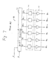
- the row electrode driving circuit 62 comprises a shift register circuit 71, a level shifter circuit 72, and a buffer circuit 73.
- the shift register circuit 71 shifts a pulse signal D in accordance with clock pulses ⁇ and sequentially outputs the pulse signal to lines q 1 , q 2 , ..., q n .
- the level shifter circuit 72 converts the pulse signal output to the lines q 1 , q 2 , ..., q n into voltage levels required for turning on and off the switching transistors 61d.
- the buffer circuit 73 outputs voltage signals Q 1 , Q 2 , ..., Q n converted by level shifter circuit 72.
- pulse signals are sequentially output to the lines q 1 , q 2 , ..., q n from the shift register circuit 71.
- the voltage signals Q 1 , Q 2 , ..., Q n converted by level shifter circuit 72 are output through the buffer circuit 73, based on this pulse signal.
- the row electrode driving circuit 62 is usually comprised of a plurality of partial row electrode driving circuits 90a (LS11), 90b (LSI2), 90c (LS13), ..., each corresponding to a portion of the row electrodes 61a and integrated in one LSI chip, as shown in Figure 9.
- the partial row electrode driving circuits 90a, 90b, 90c, ... comprise shift register circuits 91a, 91b, 91c, ... (hereinafter, simply indicated by “91"), level shifter circuits 92a, 92b, 92c, ... (hereinafter, simply indicated by “92”), and buffer circuits 93a, 93b, 93c, ...
- the shift register circuit91, level shifter circuit 92 and buffer circuit 93 may have the same structure as the shift register circuit 71, level shifter circuit 72 and buffer circuit 73 shown in Figure 7, respectively, except that the number of row electrodes to drive is different. It is necessary for the shift register circuits 91a, 91b, 91c, ... in all of the partial row electrode driving circuits 90, as a whole, to continuously operate as a single shift register circuit. Therefore, for example, the output of the final step of the shift register circuit 91a in the partial row electrode driving circuit 90a is supplied to the shift register circuit 91b in the next partial row electrode driving circuit 90b.
- the row electrode driving circuit for a display apparatus of this invention comprises a plurality of partial row electrode driving circuits which respectively drive groups of row electrodes of said display apparatus, each of said partial row electrode driving circuits is allocated with a number, and comprises: shift register means for shifting a pulse signal to sequentially output said pulse signal from a plurality of outputs, the shifting direction being changeable in accordance with a shift direction control signal; count means for counting clock pulses, and for producing a count signal at each time when a predetermined number of clock pulses have been counted; switch means for, when said shift direction is set to a first direction, producing a signal indicating said allocated number, and for, when said shift direction is set to a second direction which is opposite to said first direction, producing a signal indicating a number which is obtained by subtracting said allocated number from a specified number; and pulse signal output means for, when said number output from said switch means and the number of said count signals satisfy a predetermined relationship
- said display apparatus is a matrix type liquid crystal display apparatus.
- said predetermined number of clock pulses is the number of steps of said shift register means.
- said allocated number of one of said partial row electrode driving circuits corresponds to the position of said partial row electrode driving circuit in the arrangement of said partial row electrode driving circuits.
- said specified number relates to the number of said partial row electrode driving circuits.
- Figure 2 illustrates a row electrode driving circuit according to the invention.
- the circuit of Figure 2 can drive the LCD apparatus shown in Figure 6, and comprises four partial row electrode driving circuits 10a, 10b, 10c and 10d (hereinafter, simply indicated by "10" when the partial row electrode driving circuits are collectively referred), each of which corresponds to k number of row electrodes in the LCD apparatus.
- the number of partial row electrode driving circuits 10 and the number of row electrodes which correspond to one of the partial row electrode driving circuits 10 are not restricted to the above and can be selected arbitrarily.
- the partial row electrode driving circuits 10a, 10b, 10c and 10d each of which is integrated into one LSI chip (LS11, LSI2, LS13, LSI4) comprise shift register circuits 11a, 11b, 11c and 11d (hereinafter, simply indicated by “11"), level shifter circuits 12a, 12b, 12c and 12d (hereinafter, simply indicated by “12"), buffer circuits 13a, 13b, 13c and 13d (hereinafter, simply indicated by “13”), and shift register control circuits 14a, 14b, 14c and 14d (hereinafter, simply indicated by “14"), respectively.
- Clock pulses and shift direction control signal U/L are supplied in common to the shift register circuits 11 and shift register control circuits 14 in all of the partial row electrode driving circuits 10.
- a start signal S is further supplied to the shift register control circuits 14.
- FIG 1 shows one of the partial row electrode driving circuits 10 in more detail.
- the level shifter circuit 12 and buffer circuit 13 are constructed in the same manner as those used in the prior art (i.e., the level shifter circuit 72 and buffer circuit 73 shown in Figure 7).
- the shift register circuit 11 is structured so that the shift direction reverses in response to the shift direction control signal U/L.
- the shift direction control signal U/L is U
- the normal shifting operation toward the right in Figures 1 and 2
- the pulse signals are sequentially output to the lines q 1 , q 2 , ..., in this order.
- the shift direction control signal U/L is L
- the shifting operation toward the left is performed, and the pulse signals are sequentially output to the lines q k , q k-1 , ..., in this order.
- the pulse signal D which is input to the shift register circuit 11 is supplied from outside of the partial row electrode driving circuit 10.
- the pulse signal D is generated by the shift register control circuit 14.
- the shift register control circuit 14 comprises a count circuit 15, a timing selection circuit 16, and a switching circuit 17.
- the count circuit 15 supplies a count signal C to the timing selection circuit 16 immediately after receiving the start signal S, and every time k clock pulses ⁇ (k is the number of steps in the shift register circuit 11) are counted after the input of the start signal S.
- the switching circuit 17 supplies externally established data f , when the shift direction control signal U/L is U, and data (n - 1 - f), when the shift direction control signal U/L is L, to the timing selection circuit 16.
- Data supplied from the switching circuit 17 to the timing selection circuit 16 is representatively indicated by f' in Figure 1.
- f' f
- the shift direction control signal U/L U
- f' (n - 1 - f).
- the timing selection circuit 16 outputs the pulse signal D to the shift register circuit 11 when the number of count signals C which have been input is equal to (f' + 1).
- FIG. 3 is the timing chart for a case in which the shift direction control signal U/L is U.
- one count signal C ((c) of Figure 3) is first generated by the count circuit 15.
- one count signal C is generated every time k number of clock pulses ⁇ ((a) of Figure 3) are input.
- the time interval t k for generating the count signal C is equal to the period of time required for shifting the pulse signal D through all of the steps of the shift register circuit 11.
- subscripts 0 to 3 are added to the pulse signal D in accordance with the values (0 to 3) of the data f which are assigned to the partial row electrode driving circuits 10, in the same way as in Figure 2.
- the shift register control circuit 14 can generate the pulse signal which is directed to the shift register circuit 11 within the same partial row electrode driving circuit 10, with proper timing based upon the data f. Therefore, in this embodiment, the pulse signals Do, D i , D 2 and D 3 are handled within each partial row electrode driving circuit 10.
- the digital signals which are transmitted between the partial row electrode driving circuits in a row electrode driving circuit of the prior art are not necessary, and thus it is possible to avoid image disturbance due to noises from the digital signals.
- the level of the start signal S changes outside of the image display period, and the start signal S can be generated outside of the LSI which contains the partial row electrode driving circuit 10. Hence, it is possible to easily add a circuit as a noise countermeasure, so that the start signal S does not become a source of image disturbance.
- Figure 4 illustrates the operation of this embodiment in the case where the shift direction control signal U/L is L.
- the shift direction control signal U/L is L
- the generation sequence of the pulse signals Do through D 3 is opposite to that in the case where the shift direction control signal U/L is U ((d) to (g) of Figure 3).
- the direction in which the pulse signal D is shifted by the shift register circuit 11 within the partial row electrode driving circuit 10 is also opposite to that in the case where the shift direction control signal U/L is U.
- FIG. 5 An example of the shift register control circuit 14 is shown in Figure 5.
- the value k is set to 64, and data f is expressed with two bits (f 1 , lo).
- the shift direction control signal U/L is U, it has the value of "0", and when the shift direction control signal U/L is L, it has the value of "1".
- the count signal C which is generated immediately after the input of the start signal S is output from a D-type flip-flop 152.
- the count signal C which is output from the OR gate 154 is counted by a 1/4 counter 161.
- the count signal C is output from the D-type flip-flop 152 or the OR gate 154, it is determined by the combination of NOR gates 162-165 whether or not the data f' expressed by two bits (f 1 ', fol) and supplied from the switching circuit 17 coincide with the output of the 1/4 counter 161. If yes, the pulse signal D is output from an OR gate 166.
- the invention it is not necessary to produce digital signals between partial row electrode driving circuits. In the row electrode driving circuits of the invention, therefore, image disturbance due to noises resulting from digital signals can be eliminated. Furthermore, in the row electrode driving circuits of the invention, the sequence of driving row electrodes in a display apparatus can be easily reversed by controlling the shift direction control signal.
Landscapes
- Engineering & Computer Science (AREA)
- Chemical & Material Sciences (AREA)
- Crystallography & Structural Chemistry (AREA)
- Physics & Mathematics (AREA)
- Computer Hardware Design (AREA)
- General Physics & Mathematics (AREA)
- Theoretical Computer Science (AREA)
- Liquid Crystal Display Device Control (AREA)
- Control Of Indicators Other Than Cathode Ray Tubes (AREA)
- Liquid Crystal (AREA)
Abstract
Description
- This invention relates to a row electrode driving circuit for a display apparatus, and more particularly to a row electrode driving circuit for a matrix type display apparatus.
- As a typical example of a matrix type display device, a matrix type liquid crystal display (LCD) apparatus is shown in Figure 6. The LCD apparatus of Figure 6 comprises an
LCD panel 61 having: a plurality of row electrodes 61a which are disposed on a substrate parallel to one another; and a plurality ofcolumn electrodes 61b which intersect the row electrodes 61a. A pair of a picture element (pixel)electrode 61c and a thin film transistor (TFT) 61d which functions as a switching element is disposed at each crossing of the row electrodes 61a and thecolumn electrodes 61b. TheLCD panel 61 is driven by a rowelectrode driving circuit 62 and columnelectrode driving circuit 63. The rowelectrode driving circuit 62 produces scanning pulses which are in turn supplied to the row electrodes 61a to sequentially turn on each row of the switching transistors 61d. The columnelectrode driving circuit 63 produces voltage signals which are applied to thepixel electrodes 61 c through thecolumn electrodes 61b. A control circuit 64 controls the operations of the rowelectrode driving circuit 62 and the columnelectrode driving circuit 63. - As shown in Figure 7, the row
electrode driving circuit 62 comprises ashift register circuit 71, alevel shifter circuit 72, and abuffer circuit 73. Theshift register circuit 71 shifts a pulse signal D in accordance with clock pulses φ and sequentially outputs the pulse signal to lines q1, q2, ..., qn. Thelevel shifter circuit 72 converts the pulse signal output to the lines q1, q2, ..., qn into voltage levels required for turning on and off the switching transistors 61d. Thebuffer circuit 73 outputs voltage signals Q1, Q2, ..., Qn converted bylevel shifter circuit 72. - The operation of the row
electrode driving circuit 62 will be described with reference to Figure 8. After the input of the pulse signal D, pulse signals are sequentially output to the lines q1, q2, ..., qn from theshift register circuit 71. The voltage signals Q1, Q2, ..., Qn converted bylevel shifter circuit 72 are output through thebuffer circuit 73, based on this pulse signal. - If the number of the row electrodes 61 a to be driven is large, the row
electrode driving circuit 62 is usually comprised of a plurality of partial rowelectrode driving circuits 90a (LS11), 90b (LSI2), 90c (LS13), ..., each corresponding to a portion of the row electrodes 61a and integrated in one LSI chip, as shown in Figure 9. The partial rowelectrode driving circuits 90a, 90b, 90c, ... compriseshift register circuits 91a, 91b, 91c, ... (hereinafter, simply indicated by "91"),level shifter circuits 92a, 92b, 92c, ... (hereinafter, simply indicated by "92"), andbuffer circuits shift register circuit 71,level shifter circuit 72 andbuffer circuit 73 shown in Figure 7, respectively, except that the number of row electrodes to drive is different. It is necessary for theshift register circuits 91a, 91b, 91c, ... in all of the partial rowelectrode driving circuits 90, as a whole, to continuously operate as a single shift register circuit. Therefore, for example, the output of the final step of the shift register circuit 91a in the partial rowelectrode driving circuit 90a is supplied to the shift register circuit 91b in the next partial row electrode driving circuit 90b. - In the above-mentioned row
electrode driving circuit 62, digital signals and analog signals mixedly exist, and therefore noises from the digital signals which are mixed with the analog signals become a problem. When such a rowelectrode driving circuit 62 is applied to a display apparatus in a small sized television display device, in addition to a direct effect via power lines and signal lines, there occurs such an indirect effect that high frequency noises radiated into the air are picked up by an antenna of the device, causing disturbance in the displayed image. Furthermore, at the instant when the level of the digital signals changes, currents of a comparatively large amount flow, and as a result, a linear disturbance synchronized with the change in the digital signal level is generated on the display of the display apparatus. In a row electrode driving circuit as shown in Figure 9 wherein a plurality of partial row electrode driving circuits (LSls) are connected in a cascade, the level of digital signals transmitted between the LSls change during an image display period, thereby causing the image disturbance. Furthermore, since LSls are usually mounted in a high density, there are many cases where it is impossible to carry out effective noise countermeasures in the vicinity of the LSls. - The row electrode driving circuit for a display apparatus of this invention, which overcomes the above-discussed and numerous other disadvantages and deficiencies of the prior art, comprises a plurality of partial row electrode driving circuits which respectively drive groups of row electrodes of said display apparatus, each of said partial row electrode driving circuits is allocated with a number, and comprises: shift register means for shifting a pulse signal to sequentially output said pulse signal from a plurality of outputs, the shifting direction being changeable in accordance with a shift direction control signal; count means for counting clock pulses, and for producing a count signal at each time when a predetermined number of clock pulses have been counted; switch means for, when said shift direction is set to a first direction, producing a signal indicating said allocated number, and for, when said shift direction is set to a second direction which is opposite to said first direction, producing a signal indicating a number which is obtained by subtracting said allocated number from a specified number; and pulse signal output means for, when said number output from said switch means and the number of said count signals satisfy a predetermined relationship, outputting said pulse signal.
- Preferably, said display apparatus is a matrix type liquid crystal display apparatus.
- Preferably, said predetermined number of clock pulses is the number of steps of said shift register means.
- Preferably, said allocated number of one of said partial row electrode driving circuits corresponds to the position of said partial row electrode driving circuit in the arrangement of said partial row electrode driving circuits.
- Preferably, said specified number relates to the number of said partial row electrode driving circuits.
- Thus, the invention described herein makes possible the objectives of:
- (1) providing a row electrode driving circuit which can drive a display apparatus without impairing the display quality;
- (2) providing a row electrode driving circuit which can drive a display apparatus without requiring digital signals transmitted between partial row electrode driving circuits; and
- (3) providing a row electrode driving circuit which can drive a display apparatus without producing noises caused by digital signals transmitted between partial electrode driving circuits.
- This invention may be better understood and its numerous objects and advantages will become apparent to those skilled in the art by reference to the accompanying drawings as follows:
- Figure 1 is a block diagram illustrating a partial row electrode driving circuit used in a row electrode driving circuit according to the invention.
- Figure 2 is a block diagram illustrating the row electrode driving circuit according to the invention.
- Figures 3 and 4 are timing charts illustrating the operation of the row electrode driving circuit of Figure 2.
- Figure 5 is a circuit diagram illustrating an example of a shift register control circuit in detail used in the partial row electrode driving circuit of Figure 1.
- Figure 6 diagrammatically illustrates a matrix type LCD apparatus of the prior art.
- Figure 7 is a block diagram illustrating a row electrode driving circuit of the prior art.
- Figure 8 is a timing chart illustrating the operation of the row electrode driving circuit of Figure 7.
- Figure 9 shows the configuration of the prior art row electrode driving circuit comprising a plurality of partial row electrode driving circuits.
- Figure 2 illustrates a row electrode driving circuit according to the invention. The circuit of Figure 2 can drive the LCD apparatus shown in Figure 6, and comprises four partial row
electrode driving circuits electrode driving circuits 10 and the number of row electrodes which correspond to one of the partial rowelectrode driving circuits 10 are not restricted to the above and can be selected arbitrarily. The partial rowelectrode driving circuits shift register circuits 11a, 11b, 11c and 11d (hereinafter, simply indicated by "11"),level shifter circuits 12a, 12b, 12c and 12d (hereinafter, simply indicated by "12"),buffer circuits 13a, 13b, 13c and 13d (hereinafter, simply indicated by "13"), and shiftregister control circuits 14a, 14b, 14c and 14d (hereinafter, simply indicated by "14"), respectively. Clock pulses and shift direction control signal U/L are supplied in common to theshift register circuits 11 and shiftregister control circuits 14 in all of the partial rowelectrode driving circuits 10. A start signal S is further supplied to the shiftregister control circuits 14. - Figure 1 shows one of the partial row
electrode driving circuits 10 in more detail. Thelevel shifter circuit 12 andbuffer circuit 13 are constructed in the same manner as those used in the prior art (i.e., thelevel shifter circuit 72 andbuffer circuit 73 shown in Figure 7). Theshift register circuit 11 is structured so that the shift direction reverses in response to the shift direction control signal U/L. When the shift direction control signal U/L is U, the normal shifting operation toward the right (in Figures 1 and 2) is performed, and the pulse signals are sequentially output to the lines q1, q2, ..., in this order. When the shift direction control signal U/L is L, the shifting operation toward the left is performed, and the pulse signals are sequentially output to the lines qk, qk-1, ..., in this order. In the prior art, the pulse signal D which is input to theshift register circuit 11 is supplied from outside of the partial rowelectrode driving circuit 10. By contrast, in this embodiment, the pulse signal D is generated by the shiftregister control circuit 14. - The shift
register control circuit 14 comprises acount circuit 15, atiming selection circuit 16, and aswitching circuit 17. Thecount circuit 15 supplies a count signal C to thetiming selection circuit 16 immediately after receiving the start signal S, and every time k clock pulses φ (k is the number of steps in the shift register circuit 11) are counted after the input of the start signal S. Theswitching circuit 17 supplies externally established data f , when the shift direction control signal U/L is U, and data (n - 1 - f), when the shift direction control signal U/L is L, to thetiming selection circuit 16. Here, n is the total number of the partial rowelectrode driving circuits 10, and in this embodiment n = 4. As shown in Figure 2, f is a value assigned to each of the partial row electrode driving circuits 10a (f = 0), 10b (f = 1), 10c (f = 2) and 10d (f = 3), based upon the arrangement order in which the partial rowelectrode driving circuits 10 are disposed. Data supplied from the switchingcircuit 17 to thetiming selection circuit 16 is representatively indicated by f' in Figure 1. In other words, when the shift direction control signal U/L is U, f' = f , and when the shift direction control signal U/L is L, f' = (n - 1 - f). Thetiming selection circuit 16 outputs the pulse signal D to theshift register circuit 11 when the number of count signals C which have been input is equal to (f' + 1). - The operation of this embodiment will be described with reference to Figure 3 which is the timing chart for a case in which the shift direction control signal U/L is U. Immediately after receiving the start signal S ((b) of Figure 3), one count signal C ((c) of Figure 3) is first generated by the
count circuit 15. Following this, one count signal C is generated every time k number of clock pulses φ ((a) of Figure 3) are input. The time interval tk for generating the count signal C is equal to the period of time required for shifting the pulse signal D through all of the steps of theshift register circuit 11. In (d) to (g) of Figure 3,subscripts 0 to 3 are added to the pulse signal D in accordance with the values (0 to 3) of the data f which are assigned to the partial rowelectrode driving circuits 10, in the same way as in Figure 2. - As seen from the above description, according to this embodiment, the shift
register control circuit 14 can generate the pulse signal which is directed to theshift register circuit 11 within the same partial rowelectrode driving circuit 10, with proper timing based upon the data f. Therefore, in this embodiment, the pulse signals Do, Di, D2 and D3 are handled within each partial rowelectrode driving circuit 10. In other words, in this embodiment, the digital signals which are transmitted between the partial row electrode driving circuits in a row electrode driving circuit of the prior art are not necessary, and thus it is possible to avoid image disturbance due to noises from the digital signals. Moreover, the level of the start signal S changes outside of the image display period, and the start signal S can be generated outside of the LSI which contains the partial rowelectrode driving circuit 10. Hence, it is possible to easily add a circuit as a noise countermeasure, so that the start signal S does not become a source of image disturbance. - Figure 4 illustrates the operation of this embodiment in the case where the shift direction control signal U/L is L. When the shift direction control signal U/L is L, as shown in (d) to (g) of Figure 4, the generation sequence of the pulse signals Do through D3 is opposite to that in the case where the shift direction control signal U/L is U ((d) to (g) of Figure 3). Furthermore, although not illustrated, the direction in which the pulse signal D is shifted by the
shift register circuit 11 within the partial rowelectrode driving circuit 10 is also opposite to that in the case where the shift direction control signal U/L is U. - An example of the shift
register control circuit 14 is shown in Figure 5. In the shiftregister control circuit 14, the value k is set to 64, and data f is expressed with two bits (f1, ℓo). When the shift direction control signal U/L is U, it has the value of "0", and when the shift direction control signal U/L is L, it has the value of "1". The count signal C which is generated immediately after the input of the start signal S is output from a D-type flip-flop 152. A 1/64counter 151 counts the clock pulses ϕ. When the output of the 1/64counter 151 changes from 63 (= 111111) to 0 (= 000000), the count signal C is output from an OR gate 154. The count signal C which is output from the OR gate 154 is counted by a 1/4counter 161. When the count signal C is output from the D-type flip-flop 152 or the OR gate 154, it is determined by the combination of NOR gates 162-165 whether or not the data f' expressed by two bits (f1', fol) and supplied from the switchingcircuit 17 coincide with the output of the 1/4counter 161. If yes, the pulse signal D is output from anOR gate 166. - According to the invention, it is not necessary to produce digital signals between partial row electrode driving circuits. In the row electrode driving circuits of the invention, therefore, image disturbance due to noises resulting from digital signals can be eliminated. Furthermore, in the row electrode driving circuits of the invention, the sequence of driving row electrodes in a display apparatus can be easily reversed by controlling the shift direction control signal.
- It is understood that various other modifications will be apparent to and can be readily made by those skilled in the art without departing from the scope and spirit of this invention. Accordingly, it is not intended that the scope of the claims appended hereto be limited to the description as set forth herein, but rather that the claims be construed as encompassing all the features of patentable novelty that reside in the present invention, including all features that would be treated as equivalents thereof by those skilled in the art to which this invention pertains.
Claims (9)
Applications Claiming Priority (2)
| Application Number | Priority Date | Filing Date | Title |
|---|---|---|---|
| JP296164/90 | 1990-10-31 | ||
| JP2296164A JPH04168477A (en) | 1990-10-31 | 1990-10-31 | Display device row electrode drive circuit |
Publications (3)
| Publication Number | Publication Date |
|---|---|
| EP0484164A2 true EP0484164A2 (en) | 1992-05-06 |
| EP0484164A3 EP0484164A3 (en) | 1992-10-28 |
| EP0484164B1 EP0484164B1 (en) | 1996-01-31 |
Family
ID=17829988
Family Applications (1)
| Application Number | Title | Priority Date | Filing Date |
|---|---|---|---|
| EP91310092A Expired - Lifetime EP0484164B1 (en) | 1990-10-31 | 1991-10-31 | A row electrode driving circuit for a display apparatus |
Country Status (6)
| Country | Link |
|---|---|
| US (1) | US5253093A (en) |
| EP (1) | EP0484164B1 (en) |
| JP (1) | JPH04168477A (en) |
| KR (1) | KR960008102B1 (en) |
| DE (1) | DE69116798T2 (en) |
| TW (1) | TW211069B (en) |
Cited By (2)
| Publication number | Priority date | Publication date | Assignee | Title |
|---|---|---|---|---|
| GB2383699A (en) * | 2001-12-12 | 2003-07-02 | Lg Philips Lcd Co Ltd | An LCD panel with integrated row and data signal pulse generating shift registers and shift register output level shifters |
| TWI413986B (en) * | 2009-07-01 | 2013-11-01 | Au Optronics Corp | Shift registers |
Families Citing this family (4)
| Publication number | Priority date | Publication date | Assignee | Title |
|---|---|---|---|---|
| DE69311930T2 (en) * | 1992-01-31 | 1997-11-20 | Canon Kk | Liquid crystal light valve with active matrix and driver circuit |
| US5532712A (en) * | 1993-04-13 | 1996-07-02 | Kabushiki Kaisha Komatsu Seisakusho | Drive circuit for use with transmissive scattered liquid crystal display device |
| JP3059048B2 (en) * | 1994-05-19 | 2000-07-04 | シャープ株式会社 | Liquid crystal display device and driving method thereof |
| JPH08106272A (en) * | 1994-10-03 | 1996-04-23 | Semiconductor Energy Lab Co Ltd | Display device driving circuit |
Family Cites Families (9)
| Publication number | Priority date | Publication date | Assignee | Title |
|---|---|---|---|---|
| JPS54126497A (en) * | 1978-03-24 | 1979-10-01 | Sharp Corp | Dap-type liquid crystal display device |
| JPS58216289A (en) * | 1982-06-10 | 1983-12-15 | シャープ株式会社 | LCD display drive circuit |
| DE3380465D1 (en) * | 1982-09-20 | 1989-09-28 | Toshiba Kk | Video ram write control apparatus |
| JPS6132093A (en) * | 1984-07-23 | 1986-02-14 | シャープ株式会社 | LCD drive circuit |
| ES2044845T3 (en) * | 1986-02-17 | 1994-01-16 | Canon Kk | EXCITING DEVICE. |
| JPH061312B2 (en) * | 1986-02-20 | 1994-01-05 | 富士写真フイルム株式会社 | LCD drive controller |
| DE3854163T2 (en) * | 1987-01-09 | 1996-04-04 | Hitachi Ltd | Method and circuit for sensing capacitive loads. |
| JPH0654421B2 (en) * | 1987-12-07 | 1994-07-20 | シャープ株式会社 | Column electrode driving circuit of matrix type liquid crystal display device |
| JPH03198087A (en) * | 1989-12-27 | 1991-08-29 | Sharp Corp | Column electrode drive circuit for display devices |
-
1990
- 1990-10-31 JP JP2296164A patent/JPH04168477A/en active Pending
-
1991
- 1991-10-29 TW TW080108476A patent/TW211069B/zh active
- 1991-10-29 US US07/783,890 patent/US5253093A/en not_active Expired - Lifetime
- 1991-10-31 DE DE69116798T patent/DE69116798T2/en not_active Expired - Fee Related
- 1991-10-31 EP EP91310092A patent/EP0484164B1/en not_active Expired - Lifetime
- 1991-11-04 KR KR1019910019503A patent/KR960008102B1/en not_active Expired - Fee Related
Cited By (4)
| Publication number | Priority date | Publication date | Assignee | Title |
|---|---|---|---|---|
| GB2383699A (en) * | 2001-12-12 | 2003-07-02 | Lg Philips Lcd Co Ltd | An LCD panel with integrated row and data signal pulse generating shift registers and shift register output level shifters |
| GB2383699B (en) * | 2001-12-12 | 2004-08-18 | Lg Philips Lcd Co Ltd | A shift register with a built in level shifter |
| US7050036B2 (en) | 2001-12-12 | 2006-05-23 | Lg.Philips Lcd Co., Ltd. | Shift register with a built in level shifter |
| TWI413986B (en) * | 2009-07-01 | 2013-11-01 | Au Optronics Corp | Shift registers |
Also Published As
| Publication number | Publication date |
|---|---|
| KR960008102B1 (en) | 1996-06-19 |
| US5253093A (en) | 1993-10-12 |
| EP0484164A3 (en) | 1992-10-28 |
| JPH04168477A (en) | 1992-06-16 |
| KR920009212A (en) | 1992-05-28 |
| EP0484164B1 (en) | 1996-01-31 |
| DE69116798T2 (en) | 1996-06-27 |
| TW211069B (en) | 1993-08-11 |
| DE69116798D1 (en) | 1996-03-14 |
Similar Documents
| Publication | Publication Date | Title |
|---|---|---|
| US5172108A (en) | Multilevel image display method and system | |
| US5103218A (en) | Source electrode driving circuit for matrix type liquid crystal display apparatus | |
| EP0295802B1 (en) | Liquid crystal display device | |
| KR100301545B1 (en) | Drive circuit for an active matrix liquid crystal display device | |
| US5307084A (en) | Method and apparatus for driving a liquid crystal display panel | |
| US5886679A (en) | Driver circuit for driving liquid-crystal display | |
| US4702560A (en) | Liquid crystal display device | |
| US9805637B2 (en) | Display devices for compensating for kickback-voltage effect | |
| US4785297A (en) | Driver circuit for matrix type display device | |
| US7253810B2 (en) | Liquid crystal display having data driver and gate driver | |
| US5166670A (en) | Column electrode driving circuit for a display apparatus | |
| US20020093494A1 (en) | Flat display unit | |
| JP3637898B2 (en) | Display driving circuit and display panel having the same | |
| US7746306B2 (en) | Display device having an improved video signal drive circuit | |
| US5253093A (en) | Row electrode driving circuit for a display apparatus | |
| US5132678A (en) | Display device with time-multiplexed addressing of groups of rows of pixels | |
| JP4984337B2 (en) | Display panel drive circuit and display device | |
| KR100391734B1 (en) | Display apparatus in which blanking data is written during blanking period | |
| KR20040024915A (en) | Liquid crystal display | |
| US5315315A (en) | Integrated circuit for driving display element | |
| US5786800A (en) | Display device | |
| JPH05108030A (en) | Driving circuit for liquid crystal panel | |
| JPH02210323A (en) | Driving circuit for matrix circuit and clock forming device for controlling its driving circuit | |
| EP0544427A2 (en) | Display module drive circuit having a digital source driver capable of generating multi-level drive voltages from a single external power source | |
| JPH0534409A (en) | Test mode control signal generating circuit |
Legal Events
| Date | Code | Title | Description |
|---|---|---|---|
| PUAI | Public reference made under article 153(3) epc to a published international application that has entered the european phase |
Free format text: ORIGINAL CODE: 0009012 |
|
| AK | Designated contracting states |
Kind code of ref document: A2 Designated state(s): DE FR GB IT NL |
|
| PUAL | Search report despatched |
Free format text: ORIGINAL CODE: 0009013 |
|
| AK | Designated contracting states |
Kind code of ref document: A3 Designated state(s): DE FR GB IT NL |
|
| 17P | Request for examination filed |
Effective date: 19921218 |
|
| 17Q | First examination report despatched |
Effective date: 19940728 |
|
| GRAA | (expected) grant |
Free format text: ORIGINAL CODE: 0009210 |
|
| AK | Designated contracting states |
Kind code of ref document: B1 Designated state(s): DE FR GB IT NL |
|
| ITF | It: translation for a ep patent filed | ||
| REF | Corresponds to: |
Ref document number: 69116798 Country of ref document: DE Date of ref document: 19960314 |
|
| ET | Fr: translation filed | ||
| PLBE | No opposition filed within time limit |
Free format text: ORIGINAL CODE: 0009261 |
|
| STAA | Information on the status of an ep patent application or granted ep patent |
Free format text: STATUS: NO OPPOSITION FILED WITHIN TIME LIMIT |
|
| 26N | No opposition filed | ||
| PGFP | Annual fee paid to national office [announced via postgrant information from national office to epo] |
Ref country code: FR Payment date: 20011010 Year of fee payment: 11 |
|
| PGFP | Annual fee paid to national office [announced via postgrant information from national office to epo] |
Ref country code: NL Payment date: 20011031 Year of fee payment: 11 Ref country code: GB Payment date: 20011031 Year of fee payment: 11 |
|
| PGFP | Annual fee paid to national office [announced via postgrant information from national office to epo] |
Ref country code: DE Payment date: 20011112 Year of fee payment: 11 |
|
| REG | Reference to a national code |
Ref country code: GB Ref legal event code: IF02 |
|
| PG25 | Lapsed in a contracting state [announced via postgrant information from national office to epo] |
Ref country code: GB Free format text: LAPSE BECAUSE OF NON-PAYMENT OF DUE FEES Effective date: 20021031 |
|
| PG25 | Lapsed in a contracting state [announced via postgrant information from national office to epo] |
Ref country code: NL Free format text: LAPSE BECAUSE OF NON-PAYMENT OF DUE FEES Effective date: 20030501 Ref country code: DE Free format text: LAPSE BECAUSE OF NON-PAYMENT OF DUE FEES Effective date: 20030501 |
|
| GBPC | Gb: european patent ceased through non-payment of renewal fee | ||
| PG25 | Lapsed in a contracting state [announced via postgrant information from national office to epo] |
Ref country code: FR Free format text: LAPSE BECAUSE OF NON-PAYMENT OF DUE FEES Effective date: 20030630 |
|
| NLV4 | Nl: lapsed or anulled due to non-payment of the annual fee |
Effective date: 20030501 |
|
| REG | Reference to a national code |
Ref country code: FR Ref legal event code: ST |
|
| PG25 | Lapsed in a contracting state [announced via postgrant information from national office to epo] |
Ref country code: IT Free format text: LAPSE BECAUSE OF NON-PAYMENT OF DUE FEES;WARNING: LAPSES OF ITALIAN PATENTS WITH EFFECTIVE DATE BEFORE 2007 MAY HAVE OCCURRED AT ANY TIME BEFORE 2007. THE CORRECT EFFECTIVE DATE MAY BE DIFFERENT FROM THE ONE RECORDED. Effective date: 20051031 |