EP0483662B1 - Verfahren zur Herstellung freitragender Mikrostrukturen - Google Patents
Verfahren zur Herstellung freitragender Mikrostrukturen Download PDFInfo
- Publication number
- EP0483662B1 EP0483662B1 EP91118109A EP91118109A EP0483662B1 EP 0483662 B1 EP0483662 B1 EP 0483662B1 EP 91118109 A EP91118109 A EP 91118109A EP 91118109 A EP91118109 A EP 91118109A EP 0483662 B1 EP0483662 B1 EP 0483662B1
- Authority
- EP
- European Patent Office
- Prior art keywords
- microstructure
- layer
- microstructures
- sacrificial layer
- substrate
- Prior art date
- Legal status (The legal status is an assumption and is not a legal conclusion. Google has not performed a legal analysis and makes no representation as to the accuracy of the status listed.)
- Expired - Lifetime
Links
Images
Classifications
-
- C—CHEMISTRY; METALLURGY
- C25—ELECTROLYTIC OR ELECTROPHORETIC PROCESSES; APPARATUS THEREFOR
- C25D—PROCESSES FOR THE ELECTROLYTIC OR ELECTROPHORETIC PRODUCTION OF COATINGS; ELECTROFORMING; APPARATUS THEREFOR
- C25D1/00—Electroforming
- C25D1/08—Perforated or foraminous objects, e.g. sieves
Definitions
- the invention relates to a method for producing self-supporting microstructures according to the preamble of patent claim 1.
- microstructures are produced on a starting electroplating layer that is connected to a glass plate. The microstructures are then mechanically separated from the glass plate.
- a disadvantage of this method is that the intended shape of sensitive microstructures can easily be changed in an undesired manner during the mechanical separation from the glass plate.
- the object of the invention is to modify a method of the generic type such that microstructures can be separated from the substrate on which they were produced within a few minutes without the structures being adversely affected.
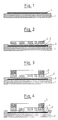
- FIGS 1 to 7 show the individual process steps.
- a separating layer 2 made of carbon was evaporated to a thickness of 20 nm on an approximately 0.5 mm thick silicon wafer as substrate 1 with a diameter of approximately 100 mm. With this carbon coating, the edge of the silicon wafer 1 was left free (FIG. 1).
- the separating layer 2 and the edge of the silicon wafer were coated with a 3 ⁇ m thick sacrificial layer 3 made of titanium by magnetron sputtering.
- the thickness of the separating layer 2 should advantageously be between 10 and 30 nm. It is also possible to sputter carbon more than approx. 50 nm to 150 nm thick by magnetron sputtering instead of evaporating it.
- the thickness of the titanium layer 3 is advantageously between 2 and 10 ⁇ m.
- These structures 4 were connected with a sapphire-filled 2-component adhesive with solid, approximately 2.5 mm thick, ring-shaped frames as a holding structure 5 made of electrolytic copper with an inner diameter of 15 mm and an outer diameter of 20 mm (FIG. 3).
- the adhesive filled with sapphire is also suitable for applications in which the connection between microstructure 4 and frame 5 has to withstand cryogenic temperatures of up to 3 K.
- Epoxy-based adhesives are also suitable for applications in which the adhesive bond is not exposed to extreme temperatures.
- an adhesive for the connection of the microstructure 4 and the holding structure 5 has the advantage that the microstructure 4 does not have to be exposed to as high temperatures as in other connection methods such as e.g. B. diffusion soldering or welding or anodic bonding.
- a microstructure 4 is connected to a holding structure 5, which consists of a different material than the microstructure 4, the use of an adhesive largely prevents the formation of thermal stresses between the microstructure 4 and the holding structure 5.
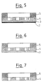
- the carbon of the separation layer 2 largely remained on the sacrificial layer and was burned in an oxygen plasma (FIG. 6).
- the microstructure 4 was integrated into a frame 5 solution immersed in hydrofluoric acid, in which the sacrificial layer 3 dissolved within a few seconds (FIG. 7).
- This method has the advantage that self-supporting microstructures can be produced and that these microstructures are stabilized when detached from the substrate by the sacrificial layer and the solid frame, so that undesired changes in the shape of the microstructures caused by the detachment from the substrate can be avoided.
- the mechanical detachment of microstructures and sacrificial layer from the substrate is facilitated in that tools can be attached to the relatively thick holding structure.
- the tensile stresses that may be present in the microstructure as a result of the production process are absorbed after the detachment from the substrate and removal of the sacrificial layer from the solid frame, so that there are no changes in shape of the microstructure.
- the large surface of the sacrificial layer accessible after detachment from the substrate and its small thickness enable the sacrificial layer to be removed quickly within a few seconds.
- a 1 mm thick lattice-shaped holding structure 5 made of stainless steel was glued to this net structure 4 with an epoxy adhesive, which was surrounded by a closed frame measuring approximately 20 ⁇ 60 mm and the spacing of the webs was approximately 15 mm with a web width of 2 mm.
- the holding structure 5 With the holding structure 5, the microstructure 4 and the copper layer 3 were removed from the glass plate 1 lifted off and the copper layer 3 in an etching solution of copper (II) chloride and ammonia selectively dissolved against the microstructure of nickel at room temperature.
- this production process has the advantage that no separating layer is required, since the copper layer also detaches from the glass plate without a separating layer.
- the use of a grid-shaped holding structure produces a very stable, self-supporting microstructure that can withstand a higher flow pressure when used as a particle filter.
- the frame around the lattice structure can also be dispensed with under certain circumstances.
- the detachment from the glass plate is then made more difficult and there is a possibility that the microstructure may be damaged during the detachment.
- the third application example describes the production of a high-pass filter in the far infrared range: on a 0.5 mm thick silicon wafer 1 with a diameter of 100 mm, a 2 ⁇ m thick titanium layer 2 was sputtered by magnetron sputtering. A 2 ⁇ m thick nickel layer 3 was electroplated onto this titanium layer 2. The electroplated nickel layer 3 adheres to the titanium layer only to a limited extent, so that the titanium layer 2 acts in this case as a separating layer.
- the diameter of the holes was 50 ⁇ m.
- the smallest distance between the edges of two holes was about 5 ⁇ m.
- this production method has the advantage that the separating layer remains completely on the silicon wafer and does not have to be removed from the nickel layer before the latter is dissolved.
Landscapes
- Chemical & Material Sciences (AREA)
- Engineering & Computer Science (AREA)
- Chemical Kinetics & Catalysis (AREA)
- Electrochemistry (AREA)
- Materials Engineering (AREA)
- Metallurgy (AREA)
- Organic Chemistry (AREA)
- Micromachines (AREA)
- Laminated Bodies (AREA)
Applications Claiming Priority (2)
| Application Number | Priority Date | Filing Date | Title |
|---|---|---|---|
| DE4034365 | 1990-10-29 | ||
| DE4034365A DE4034365A1 (de) | 1990-10-29 | 1990-10-29 | Verfahren zur herstellung freitragender mikrostrukturen |
Publications (3)
| Publication Number | Publication Date |
|---|---|
| EP0483662A2 EP0483662A2 (de) | 1992-05-06 |
| EP0483662A3 EP0483662A3 (en) | 1993-03-03 |
| EP0483662B1 true EP0483662B1 (de) | 1994-12-14 |
Family
ID=6417255
Family Applications (1)
| Application Number | Title | Priority Date | Filing Date |
|---|---|---|---|
| EP91118109A Expired - Lifetime EP0483662B1 (de) | 1990-10-29 | 1991-10-24 | Verfahren zur Herstellung freitragender Mikrostrukturen |
Country Status (2)
| Country | Link |
|---|---|
| EP (1) | EP0483662B1 (enExample) |
| DE (2) | DE4034365A1 (enExample) |
Families Citing this family (3)
| Publication number | Priority date | Publication date | Assignee | Title |
|---|---|---|---|---|
| DE4406600C1 (de) * | 1994-03-01 | 1995-04-27 | Kernforschungsz Karlsruhe | Verfahren zur Herstellung eines Filters für elektromagnetische Strahlung |
| EP1181239A1 (de) * | 1999-03-31 | 2002-02-27 | Siemens Aktiengesellschaft | Verfahren zur herstellung von freitragenden mikrostrukturen, von dünnen flachteilen oder von membranen und verwendung nach diesem verfahren hergestellter mikrostrukturen als widerstandsgitter in einer einrichtung zur messung schwacher gasströmungen |
| DE10239551A1 (de) * | 2002-08-23 | 2004-03-04 | Daimlerchrysler Ag | Filterkörper für Rußfilter |
Family Cites Families (5)
| Publication number | Priority date | Publication date | Assignee | Title |
|---|---|---|---|---|
| DE1160258B (de) * | 1961-06-13 | 1963-12-27 | Richard Steding | Verfahren zur Herstellung von Metallfolien auf galvanoplastischem Wege |
| DE1303000B (enExample) * | 1966-07-06 | 1971-01-28 | ||
| DE2512086C3 (de) * | 1975-03-19 | 1978-11-30 | Siemens Ag, 1000 Berlin Und 8000 Muenchen | Verfahren zur Herstellung freitragender, dünner Metallstrukturen |
| DE2832408A1 (de) * | 1978-07-24 | 1980-02-14 | Siemens Ag | Verfahren zur herstellung von praezisionsflachteilen, insbesondere mit mikrooeffnungen |
| DE3232499A1 (de) * | 1982-09-01 | 1984-03-01 | Philips Patentverwaltung Gmbh, 2000 Hamburg | Maske fuer die mustererzeugung in lackschichten mittels roentgenstrahllithographie und verfahren zu ihrer herstellung |
-
1990
- 1990-10-29 DE DE4034365A patent/DE4034365A1/de active Granted
-
1991
- 1991-10-24 EP EP91118109A patent/EP0483662B1/de not_active Expired - Lifetime
- 1991-10-24 DE DE59103890T patent/DE59103890D1/de not_active Expired - Fee Related
Also Published As
| Publication number | Publication date |
|---|---|
| EP0483662A3 (en) | 1993-03-03 |
| DE4034365C2 (enExample) | 1993-03-18 |
| DE4034365A1 (de) | 1992-04-30 |
| EP0483662A2 (de) | 1992-05-06 |
| DE59103890D1 (de) | 1995-01-26 |
Similar Documents
| Publication | Publication Date | Title |
|---|---|---|
| DE2453035C3 (de) | Verfahren zum Aufbringen einer metallischen Schicht in Form eines Musters auf einem mit einer ersten dünnen, metallischen Schicht überzogenen inerten Substrat | |
| EP1238312B1 (de) | Verwendung von polyimid für haftschichten, lithographisches verfahren zur herstellung von mikrobauteilen sowie verfahren zur herstellung von verbundmaterial | |
| DE60121878T2 (de) | Mikroaktuator und dessen Herstellungsverfahren | |
| DE69634010T2 (de) | Ein verfahren zum herstellen von mikrogefertigten strukturen | |
| DE69434999T2 (de) | Verfahren zur herstellung einer membran | |
| DE102007055019A1 (de) | Verfahren zum Herstellen einer nanoporösen Schicht | |
| DE10225680B4 (de) | Herstellverfahren für eine Metallschicht sowie Herstellverfahren für ein laminiertes keramisches Elektronikbauelement | |
| DE2901697C3 (de) | Verfahren zur Ausbildung von Leitungsverbindungen auf einem Substrat | |
| DE4139668A1 (de) | Mikroventil und verfahren zu dessen herstellung | |
| DE3529966C1 (de) | Verfahren zur Herstellung von Masken fuer die Roentgentiefenlithographie | |
| DE10040448A1 (de) | Halbleiterchip und Verfahren zu dessen Herstellung | |
| DE2425464C3 (de) | Verfahren zur Herstellung von Dunnschicht-Aperturblenden für Korpuskularstrahlgeräte | |
| EP0104685B1 (de) | Verfahren zur Herstellung einer Maske für die Musterzeugung in Lackschichten mittels Röntgenstrahllithographie | |
| EP1179361A1 (de) | Verfahren zur Herstellung einer Metallverbundmembran, damit hergestellte Metallverbundmembran und deren Verwendung | |
| EP0264594B1 (de) | Einrichtung zur Abstützung einer metallischen Mikrofilterfolie | |
| EP0085979B1 (de) | Verfahren zur Herstellung freitragender Metallgitterstrukturen | |
| EP0483662B1 (de) | Verfahren zur Herstellung freitragender Mikrostrukturen | |
| EP0141335A1 (de) | Verfahren zur Herstellung einer Röntgenmaske mit Metallträgerfolie | |
| EP0204099B1 (de) | Verfahren zur Herstellung einer Anordnung zur Tröpfchenerzeugung in Tintenschreibeinrichtungen | |
| WO1998015676A1 (de) | Mikromechanisches bauelement und ein verfahren zu dessen herstellung | |
| EP0957509A2 (de) | Verfahren zur Herstellung eines Bauteils, das eine mikrostrukturierte Schicht enthält | |
| DE2526382C3 (de) | Kathodenzerstäubungsverf ahren zur Herstellung geätzter Strukturen | |
| CH503121A (de) | Verfahren zur Herstellung von Metallniederschlägen durch Elektrolyse | |
| DE4406600C1 (de) | Verfahren zur Herstellung eines Filters für elektromagnetische Strahlung | |
| DE2645081A1 (de) | Verfahren zum abloesen von schichten |
Legal Events
| Date | Code | Title | Description |
|---|---|---|---|
| PUAI | Public reference made under article 153(3) epc to a published international application that has entered the european phase |
Free format text: ORIGINAL CODE: 0009012 |
|
| AK | Designated contracting states |
Kind code of ref document: A2 Designated state(s): CH DE FR GB IT LI SE |
|
| PUAL | Search report despatched |
Free format text: ORIGINAL CODE: 0009013 |
|
| AK | Designated contracting states |
Kind code of ref document: A3 Designated state(s): CH DE FR GB IT LI SE |
|
| 17P | Request for examination filed |
Effective date: 19930413 |
|
| 17Q | First examination report despatched |
Effective date: 19940304 |
|
| ITF | It: translation for a ep patent filed | ||
| GRAA | (expected) grant |
Free format text: ORIGINAL CODE: 0009210 |
|
| AK | Designated contracting states |
Kind code of ref document: B1 Designated state(s): CH DE FR GB IT LI SE |
|
| RAP2 | Party data changed (patent owner data changed or rights of a patent transferred) |
Owner name: KERNFORSCHUNGSZENTRUM KARLSRUHE GMBH |
|
| ET | Fr: translation filed | ||
| REF | Corresponds to: |
Ref document number: 59103890 Country of ref document: DE Date of ref document: 19950126 |
|
| EAL | Se: european patent in force in sweden |
Ref document number: 91118109.7 |
|
| GBT | Gb: translation of ep patent filed (gb section 77(6)(a)/1977) |
Effective date: 19950315 |
|
| PLBE | No opposition filed within time limit |
Free format text: ORIGINAL CODE: 0009261 |
|
| STAA | Information on the status of an ep patent application or granted ep patent |
Free format text: STATUS: NO OPPOSITION FILED WITHIN TIME LIMIT |
|
| PG25 | Lapsed in a contracting state [announced via postgrant information from national office to epo] |
Ref country code: GB Effective date: 19951024 |
|
| PG25 | Lapsed in a contracting state [announced via postgrant information from national office to epo] |
Ref country code: SE Effective date: 19951025 |
|
| PG25 | Lapsed in a contracting state [announced via postgrant information from national office to epo] |
Ref country code: LI Effective date: 19951031 Ref country code: CH Effective date: 19951031 |
|
| 26N | No opposition filed | ||
| REG | Reference to a national code |
Ref country code: CH Ref legal event code: PL |
|
| GBPC | Gb: european patent ceased through non-payment of renewal fee |
Effective date: 19951024 |
|
| PG25 | Lapsed in a contracting state [announced via postgrant information from national office to epo] |
Ref country code: FR Effective date: 19960628 |
|
| EUG | Se: european patent has lapsed |
Ref document number: 91118109.7 |
|
| REG | Reference to a national code |
Ref country code: FR Ref legal event code: ST |
|
| PG25 | Lapsed in a contracting state [announced via postgrant information from national office to epo] |
Ref country code: IT Free format text: LAPSE BECAUSE OF NON-PAYMENT OF DUE FEES Effective date: 20051024 |
|
| PGFP | Annual fee paid to national office [announced via postgrant information from national office to epo] |
Ref country code: DE Payment date: 20071217 Year of fee payment: 17 |
|
| PG25 | Lapsed in a contracting state [announced via postgrant information from national office to epo] |
Ref country code: DE Free format text: LAPSE BECAUSE OF NON-PAYMENT OF DUE FEES Effective date: 20090501 |