EP0476444B1 - Optischer Sender/Empfänger - Google Patents
Optischer Sender/Empfänger Download PDFInfo
- Publication number
- EP0476444B1 EP0476444B1 EP91115004A EP91115004A EP0476444B1 EP 0476444 B1 EP0476444 B1 EP 0476444B1 EP 91115004 A EP91115004 A EP 91115004A EP 91115004 A EP91115004 A EP 91115004A EP 0476444 B1 EP0476444 B1 EP 0476444B1
- Authority
- EP
- European Patent Office
- Prior art keywords
- transmitting
- packet
- receiving
- data
- bus
- Prior art date
- Legal status (The legal status is an assumption and is not a legal conclusion. Google has not performed a legal analysis and makes no representation as to the accuracy of the status listed.)
- Expired - Lifetime
Links
Images


Classifications
-
- H—ELECTRICITY
- H04—ELECTRIC COMMUNICATION TECHNIQUE
- H04L—TRANSMISSION OF DIGITAL INFORMATION, e.g. TELEGRAPHIC COMMUNICATION
- H04L12/00—Data switching networks
- H04L12/28—Data switching networks characterised by path configuration, e.g. LAN [Local Area Networks] or WAN [Wide Area Networks]
- H04L12/40—Bus networks
- H04L12/40006—Architecture of a communication node
- H04L12/40013—Details regarding a bus controller
-
- H—ELECTRICITY
- H04—ELECTRIC COMMUNICATION TECHNIQUE
- H04B—TRANSMISSION
- H04B10/00—Transmission systems employing electromagnetic waves other than radio-waves, e.g. infrared, visible or ultraviolet light, or employing corpuscular radiation, e.g. quantum communication
- H04B10/40—Transceivers
-
- H—ELECTRICITY
- H04—ELECTRIC COMMUNICATION TECHNIQUE
- H04L—TRANSMISSION OF DIGITAL INFORMATION, e.g. TELEGRAPHIC COMMUNICATION
- H04L12/00—Data switching networks
- H04L12/28—Data switching networks characterised by path configuration, e.g. LAN [Local Area Networks] or WAN [Wide Area Networks]
- H04L12/40—Bus networks
- H04L12/407—Bus networks with decentralised control
- H04L12/413—Bus networks with decentralised control with random access, e.g. carrier-sense multiple-access with collision detection [CSMA-CD]
Definitions
- the present invention generally relates to optical transceivers, and more particularly to an optical transceiver which uses a U-shaped optical bus as its transmission line and carries out a control dependent on packet collision in a local area network (LAN) which employs carrier sense multiple access with collision detection (CSMA/CD).
- LAN local area network
- CSMA/CD carrier sense multiple access with collision detection
- the LAN which uses the U-shaped optical bus as its transmission line is virtually unaffected by external noise when compared to the conventional system which uses a metal cable as its transmission line.
- the restrictions on the design of the LAN system is relatively small.
- FIG.1 shows an example of a conventional LAN which uses the U-shaped optical bus as its transmission line and employs the CSMA/CD.
- a plurality of optical transceivers 80 1 through 80 N are arranged on a U-shaped optical bus 81.
- each coder/decoder part 83 i an output of the photocoupler 82 i which is provided in the going path of the optical bus 81 is coupled to a receiving internal bus 87 1 via a Manchester decoder 84, a clock adjusting circuit 85 and one channel of a serial interface adapter 86.
- the Manchester decoder 84 decodes a Manchester code included in an output signal of the photocoupler 82 i which is provided in the going path of the optical bus 81 into an non-return-to-zero (NRZ) signal.
- the clock adjusting circuit 85 absorbs the difference in the accuracies of a clock in the optical bus 81 and a clock within the coder/decoder part 83 i .
- a transmitting internal bus 87 2 which forms a pair with the receiving internal bus 87 1 is coupled to a clock adjusting circuit 88 via another channel of the serial interface adapter 86.
- An output of the clock adjusting circuit 88 is coupled to an input of the photocoupler 82 i which is provided in the returning path of the optical bus 81, via a Manchester encoder 89 which codes the NRZ signal into the Manchester code.
- the receiving internal bus 87 1 is coupled to a level shift circuit 90 which notifies a packet collision generated on the optical bus 81 to each data terminal by shifting the level at the receiving internal bus 87 1 .
- the internal buses 87 1 and 87 2 are coupled to each data terminal 92 via an AUI cable prescribed under ISO8802-3 and a transceiver module 94.
- EP-A-0 224 132 shows the features of the preamble of claim 1 but no suggestion is made regarding the problem of the amount of hardware required.
- an optical transceiver as set out in claim 1.
- the optical transceiver of the present invention it is unnecessary to provide a level shift circuit, and the common bus is used in common during the transmitting and receiving operations.
- the hardware scale of the optical transceiver is effectively reduced compared to that of the conventional optical transceiver, and the optical transceiver according to the present invention is suited for production in the form of an LSI.
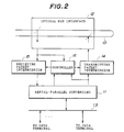
- a serial-parallel converter 11 converts receiving packets into data to be received by a data terminal (not shown) which employs the CSMA/CD and converts data transmitted from the data terminal into transmitting packets.
- An optical bus interface 12 adjusts a U-shaped optical bus 10 which is used as the transmission line to the transmitting and receiving packets.
- a common bus 13 functions as a data transfer line between the data terminal and the serial-parallel converter 11 when carrying out transmitting and receiving operations.
- a transmitting packet intermission part 14 intermits the transmitting packets in response to a transmission control signal.
- a receiving packet intermission part 15 intermits the receiving packets in response to a reception control signal.
- a controller 16 generates the transmission control signal and the reception control signal based on the timings of the transmitting and receiving packets, the relationship between the transmitting packet and the corresponding receiving packet which is looped back by the U-shaped optical bus 10 and a notification regarding a collision on the common bus 13.
- the serial-parallel converter 11 sends the notification regarding the collision on the common bus 13 based on the impedance of the common bus 13.
- the serial-parallel converter 11 converts the data which is received from the data terminal via the common bus 13 into transmitting packets.
- the controller 16 detects the head of the transmitting packet and transmits the transmission control signal.
- the transmitting packet intermission part 14 supplies the transmitting packets received via the serial-parallel converter 11 to the optical bus interface 12 in response to the transmission control signal.
- the optical bus interface 12 matches the transmitting packets to the U-shaped optical bus 10 which is used as the transmission line, and transmits the transmitting packets to the U-shaped optical bus 10.
- the controller 16 maintains the transmission control signal as it is when the transmitting packet which is transmitted matches the corresponding receiving packet which is looped back and received from the U-shaped optical bus 10.
- the controller 16 stops generating the transmission control signal so that the transmitting packet intermission part 14 returns to the original state before the start of the transmission.
- the receiving packets received from the U-shaped optical bus 10 are supplied to the controller 16 via the optical bus interface 12.
- the controller 16 transmits the reception control signal when a head of the receiving packet is detected.
- the receiving packet intermission part 15 supplies the receiving packets to the serial-parallel converter 11 in response to the reception control signal.
- the serial-parallel converter 11 converts the receiving packets into a predetermined data, and the predetermined data is supplied to the data terminal via the common bus 13.
- the controller 16 stops generating the reception control signal when a tail of the receiving packet is detected so that the receiving packet intermission part 15 returns to the original state before the start of the reception.
- the controller 16 activates one of the transmitting packet intermission part 14 and the receiving packet intermission part 15 depending on the timing difference between the transmitting packet and the receiving packet.
- the controller 16 recognizes a packet collision on the U-shaped optical bus 10 when the controller 16 detects that the transmitting packet and the corresponding receiving packet looped back from the U-shaped optical bus 10 differ during the transmitting operation. In this case, the controller 16 generates the reception control signal to activate the receiving packet intermission part 15. Since the serial-parallel converter 11 supplies the data to the common bus 13 depending on the receiving packet which is received via the receiving packet intermission part 15, a collision is generated on the common bus 13 between the data from the serial-parallel converter 11 and the data from the data terminal.
- the data terminal transmits a jam signal responsive to this collision on the common bus 13, and the other optical transceivers which are located on the other side of the U-shaped optical bus 10 similarly transmit a jam signal to the U-shaped optical bus 10.
- the controller 16 stops generating the transmission control signal when a tail of the jam signal which is transmitted from the data terminal is detected, and stops generating the reception control signal when a tail of the jam signal which is received from the U-shaped optical bus 10 is detected.
- the transmitting packet intermission part 14 and the receiving packet intermission part 15 are thus respectively returned to the original states before the start of the transmission.
- the data terminal starts the transmitting operation after the receiving packet intermission part 15 is activated depending on the receiving packet which is received from the U-shaped optical bus 10, a collision is generated on the common bus 13 between the data from the data terminal and the data from the serial-parallel converter 11.
- the serial-parallel converter 11 transmits a common bus collision notification which notifies a collision on the common bus 13, depending on the impedance of the common bus 13 at the time when such a collision occurs.
- the controller 16 activates the transmitting packet intermission part 14 in response to the common bus collision notification, and thus, a packet collision is generated on the U-shaped optical bus 10.
- the data terminal transmits a jam signal depending on the collision on the common bus 13.
- the transmitting packet intermission part 14 and the receiving packet intermission part 15 are respectively returned to the original states before the start of the transmission under the control of the controller 16, according to a procedure similar to that used when a collision is generated on the common bus 13 after a packet collision is generated on the U-shaped optical bus 10.
- each data terminal transmits a jam signal depending on the collision generated on the common bus 13. Thereafter, the parts of the optical transceiver return to the original states before the start of the transmission according to a procedure similar to that described above.
- the optical transceiver uses the common bus 13 which is used in common for the transmitting and receiving operations, and there is no need to provide a level shift circuit as in the case of the conventional optical transceiver shown in FIG.1.
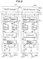
- FIG.3 those parts which are the same as those corresponding parts in FIG.1 are designated by the same reference numerals, and a description thereof will be omitted.
- each coder/decoder part 21 i is characterized in that a transmitter/receiver controller 22 is arranged between the serial interface adapter 86 and the clock adjusting circuits 85 and 88, and that a common bus 23 which is used in common for the transmitting and receiving operation is provided in place of the internal buses 87 1 and 87 2 shown in FIG.1. Furthermore, each coder/decoder part 21 i does not include the level shift circuit 90 shown in FIG.1.
- serial interface adapter 86 may be realized using an LSI AM7992B manufactured by AMD and an LSI ULA022 manufactured by TDK.
- transceiver module 94 may be realized using an LSI ULA020 manufactured by TDK.
- FIG.4 shows an embodiment of the transmitter/receiver controller 22 shown in FIG.3.
- a transmitting data (packet) which is received from the serial interface adapter 86 is supplied to one input terminal of a transmission switch part (AND gate) 32 via a transmitting data detector 31.
- An output of the transmitting switch part 32 is supplied to a first input terminal of a transmission/reception monitoring part 33 and the clock adjusting circuit 88.
- a receiving data (packet) which is received from the clock adjusting circuit 85 is supplied to a second input terminal of the transmission/reception monitoring part 33, and to one input terminal of a receiving switch part (AND gate) 35 via a receiving data detector 34.
- An output of the receiving switch part 35 is supplied to the serial interface adapter 86.
- the transmitting data detector 31 supplies to a transmission/reception select signal generator 36 a signal which indicates head and tail of the transmitting data, while the receiving data detector 34 supplies to the transmission/reception select signal generator 36 a signal which indicates head and tail of the receiving data.
- the transmission/reception select signal generator 36 generates a transmission select signal and a reception select signal based on the timings of the signals which are respectively received from the transmitting data detector 31 and the receiving data detector 34.
- the transmission select signal is supplied to the other input terminal of the transmitting switch part 32, while the reception select signal is supplied to the other input terminal of the receiving switch part 35.
- a collision detection signal which is output from the serial interface adapter 86 is supplied to a third input terminal of the transmission/reception monitoring part 33. An output of the transmission/reception monitoring part 33 is supplied to the transmission select signal generator 36.
- the photocoupler 82 1 , the Manchester decoder 84, the Manchester encoder 89 and the clock adjusting circuits 85 and 88 correspond to the optical interface 12 shown in FIG.2.
- the transmitting switch part 32 corresponds to the transmitting packet intermission part 14 shown in FIG.2, and the receiving switch part 35 corresponds to the receiving packet intermission part 15 shown in FIG.2.
- the transmitting data detector 31, the transmission/reception monitoring part 33, the receiving data detector 34 and the transmission/reception select signal generator 36 corresponds to the controller 16 shown in FIG.2.
- the serial interface adapter 86 corresponds to the serial-parallel converter 11 shown in FIG.2, and the common bus 23 corresponds to the common bus 13 shown in FIG.2.
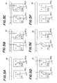
- FIGS.5A through 5F are diagrams for explaining the transmitting and receiving operations of this embodiment when no collision is generated.
- FIGS.5A through 5F show the states of the transmitting switch part 32 and the receiving switch part 35 in a simplified manner, that is, as connection states of the common bus 23 and the U-shaped optical bus 81. Such illustrations of the states of the transmitting switch part 32 and the receiving switch part 35 are also employed in FIGS.6 through 8 which will be described later.
- the transmission/reception select signal generator 36 of the coder/decoder part 21 2 activates, that is, turns ON, the transmitting switch part 32 as shown in FIG.5A when the head of this transmitting data is detected.
- the transmission/reception monitoring part 33 enters the transmitting data on the U-shaped optical bus 81 via the photocoupler 82 2 , and confirms that no packet collision is generated on the U-shaped optical bus 81 by collating the contents of the entered transmitting data with those of the transmitting data.
- the transmission/reception select signal generator 36 activates, that is, turns ON, the receiving switch part 35 when the head of a receiving data (packet) is detected as shown in FIG.5B, and supplies the receiving data to a data terminal 92 11 as shown in FIG.5C.
- the transmitting switch part When the transmitting data detector 31 detects the tail (transmission complete) of the transmitting data, the transmitting switch part is deactivated, that is, turned OFF, as shown in FIGS.5D and 5E. In addition, at the coder/decoder part 21 1 , the receiving switch part 35 is deactivated, that is, turned OFF, when the receiving data detector 34 detects the tail (reception complete) of the receiving data as shown in FIG.5F. As a result, the transmitting and receiving operation with respect to a single data (packet) is completed.
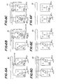
- FIGS.6A through 6F are diagrams for explaining the operation of this embodiment when a collision is generated on the U-shaped optical bus 81.
- the transmission/reception monitoring part 33 of each optical transceiver stores 512 bits including an address field of the transmitting data (packet) into a memory (not shown) when carrying out the transmitting operation.
- the transmission/reception monitoring part 33 enters the transmitting data on the U-shaped optical bus 81 via the photocoupler 82 i , and detects a data error by comparing the entered transmitting data and the transmitting data stored in the memory bit by bit. The detection of the data error corresponds to the detection of the packet collision on the U-shaped optical bus 81.
- the transmission/reception monitoring part 33 of each of the coder/decoder parts 21 1 and 21 2 notifies the above comparison result to the corresponding transmission/reception select signal generator 36.
- the transmission/reception select signal generator 36 turns ON the transmitting switch part 32 and the receiving switch part 35 simultaneously in response to this notification from the transmission/reception monitoring part 33 as shown in FIGS.6B and 6C.
- the serial interface adapter 86 transmits a predetermined data on the common bus 23 according to such a control operation, and the data from the serial interface adapter 86 and the data from the transmitting data terminal collide on the common bus 23.
- the data terminals 92 11 and 92 21 respectively detect such a collision via the AUI cable and transmit a jam signal during a jam time.
- the transmitting data detector 31 detects the stop of the jam signal transmission and turns OFF the transmitting switch part 32 as shown in FIG.6D. Furthermore, the receiving data detector 34 detects the tail of the jam signal which is received from the optical transceiver which is located on the other side of the U-shaped optical bus 81, and turns OFF the receiving switch part 35 as shown in FIGS.6E and 6E so as to return to the original state before the start of the transmission.
- FIGS.7A through 7C are diagrams for explaining the operation of this embodiment when a collision is generated on the common bus 23.
- the transmitting data detector 31 of the coder/decoder part 21 1 detects the head of the transmitting data (packet) and turns ON the transmitting switch part 32 as shown in FIG.7A when the data terminal 92 11 starts transmitting in a state where no optical transceiver makes a transmission.
- the receiving data detector 34 turns ON the receiving switch part 35 when the receiving data detector 34 detects the head of the receiving data (packet) which corresponds to the above transmitting data. But when the data terminal 92 21 simultaneously starts transmitting, the data from the serial interface adapter 86 and the data from the data terminal 92 21 collide on the common bus 23 as shown in FIG.7B.
- the serial interface adapter 86 detects this collision on the common bus 23 based on the impedance of the common bus 23, and transmits a collision detection signal to the transmission/reception monitoring part 33.
- the transmission/reception monitoring part 33 supplies a predetermined control signal to the transmission/reception select signal generator 36 in response to this collision detection signal, and the transmission/reception select signal generator 36 turns ON the transmitting switch part 32 in response to this predetermined control signal as shown in FIG.7C.
- the data terminal 92 21 detects this collision on the common bus 23 and transmits a jam data. As a result, a packet collision is generated on the U-shaped optical bus 81.
- the coder/decoder part 21 1 recognizes the collision on the common bus 23 in the coder/decoder part 21 2 indirectly from the collision on the U-shaped optical bus 81, and returns to the original state before the start of the transmission according to the procedure described above in conjunction with FIGS.6C through 6F. Furthermore, the coder/decoder part 21 2 returns to the original state before the start of the transmission according to the procedure described above in conjunction with FIGS.6D through 6F.
- FIGS.8A through 8C are diagrams for explaining the operation of this embodiment when a collision is generated on the common bus 23 due to simultaneous transmission from a plurality of data terminals.
- the serial interface adapter 86 detects this collision on the common bus 23 and transmits a collision detection signal to the transmission/reception monitoring part 33.
- the transmission/reception monitoring part 33 supplies a predetermined control signal to the transmission/reception select signal generator 36 in response to this collision detection signal, and the transmission/reception select signal generator 36 turns ON the transmitting switch part 32 and the receiving switch part 35 in response to the predetermined control signal.
- the data terminals 92 11 and 92 12 detect this collision on the common bus 23 and transmit jam data as shown in FIGS.8B and 8C.
- Each optical transceiver returns to the original state before the start of the transmission according to the procedure described above in conjunction with FIGS.6D through 6F according to the transmission end of the jam data.
- the optical transceiver does not require the level shift circuit which was conventionally required to notify the generation of the packet collision on the U-shaped optical bus, and the two internal buses which were conventionally required can be replaced by a single common bus which is used in common for the transmitting and receiving operations.
- the coder/decoder part 21 may be used as a repeater.
Landscapes
- Engineering & Computer Science (AREA)
- Computer Networks & Wireless Communication (AREA)
- Signal Processing (AREA)
- Physics & Mathematics (AREA)
- Electromagnetism (AREA)
- Small-Scale Networks (AREA)
- Optical Communication System (AREA)
Claims (14)
- Optischer Sender/Empfänger, der mit einem U-förmigen optischen Bus (10) und Datenanschlüssen gekoppelt ist und einen Trägererfassungs-Vielfachzugriff miteiner Kollisionserfassung (CSMA/CD) verwendet, wobei vorgesehen sind:- eine serielle Interface-Adaptereinrichtung (11) zum Ausführen einer Umwandlung zwischen Daten an die/von den Datenanschlüssen (N) und Sendepaketen, die von den Datenanschlüssen gesendet werden sollen, und Empfangspaketen, die von den Datenanschlüssen empfangen werden sollen, über die serielle Interface-Adaptereinrichtung;- eine Interface-Einrichtung (12) für einen optischen Bus zum Anpassen der Sende- und Empfangspakete an den U-förmigen optischen Bus, der als eine Übertragungsleitung verwendet wird;- eine Sendepaket-Abfangeinrichtung (14), die zwischen die Interface-Einrichtung für den optischen Bus und die serielle Interface-Adaptereinrichtung gekoppelt ist, zum Abfangen der Sendepakete im Ansprechen auf ein Übertragungssteuersignal;- eine Empfangspaket-Abfangeinrichtung (15), die zwischen die Interface-Einrichtung für den optischen Bus und die serielle Interface-Adaptereinrichtung gekoppelt ist, zum Abfangen der Empfangspakete im Ansprechen auf ein Empfangssteuersignal;- einen gemeinsamen Bus (13), der einen gemeinsamen Datentransferpfad zwischen der seriellen Interface-Adaptereinrichtung und den Datenanschlüssen während Sende- und Empfangsoperationen bereitstellt;- eine Steuereinrichtung (16), die zwischen die Interface-Einrichtung für den optischen Bus und die serielle Interface-Adaptereinrichtung gekoppelt ist, zum Erzeugen des Sendesteuersignals und des Empfangssteuersignals auf Grundlage von Zeitgaben des Sendepakets und des Empfangspakets und eines Zusammenhangs zwischen dem Sendepaket und einem entsprechenden Empfangspaket, welches von dem U-förmigen optischen Bus über eine Schleife zurückgeführt wird, wobei die Interface-Adaptereinrichtung eine Benachrichtigungseinrichtung zum Berichten einer Kollision auf dem gemeinsamen Bus umfaßt und dadurch gekennzeichnet ist, daß- die Benachrichtigungseinrichtung eine Kollision auf dem gemeinsamen Bus auf Grundlage einer Impedanz des gemeinsamen Busses an die Steuereinrichtung berichtet; und- die Steuereinrichtung die Sende- und Empfangssteuersignale in Abhängigkeit von der Kollisionsbenachrichtigung erzeugt;- und wobei die Steuereinrichtung (16) einen Stop in einem von den Datenanschlüssen übertragenen Blockiersignal erfaßt und eine Übertragung durch die Sendepaket-Abfangeinrichtung (14) verhindert,- und wobei die Steuereinrichtung (16) das hintere Ende des Blockiersignals in den Empfangspaketen erfaßt und eine Übertragung durch die Empfangspaket-Abfangeinrichtung (15) verhindert.
- Optischer Sender/Empfänger nach Anspruch 1 dadurch gekennzeichnet, daß während des Sendebetriebs die serielle Interface-Adaptereinrichtung (11) den Datenwert, der von dem Datenanschluß über den gemeinsamen Bus (13) empfangen wird, in die Sendepakete umwandelt, die Steuereinrichtung (16) ein vorderes Ende des Sendepakets erfaßt und das Sendesteuersignal überträgt, und die Sendepaket-Abfangeinrichtung (14) die Sendepakete, die über die Seriell-/Parallel-Umwandlungseinrichtung empfangen werden, an die Interface-Einrichtung (12) für den optischen Bus im Ansprechen auf das Sendesteuersignal liefert.
- Optischer Sender/(Empfänger nach Anspruch 2 dadurch gekennzeichnet, daß während des Sendebetriebs die Interface-Einrichtung (12) für den optischen Bus die Sendepakete an den U-förmigen optischen Bus (10) anpaßt und die Sendepakete an den U-förmigen optischen Bus überträgt.
- Optischer Sender/Empfänger nach Anspruch 3, dadurch gekennzeichnet, daß während des Sendebetriebs die Stuereinrichtung (16) das Sendesteuersignal so wie es ist aufrecht erhält, wenn das Sendepaket, das übertragen wird, mit dem entsprechenden Empfangspaket übereinstimmt, welches von dem U-förmigen optischen Bus (10) über eine Schleife zurückgeführt und empfangen wird.
- Optischer Sender/Empfänger nach Anspruch 4, dadurch gekennzeichnet, daß, wenn die Steuereinrichtung (16) ein hinteres Ende des Sendepakets erfaßt, die Steuereinrichtung eine Erzeugung des Sendesteuersignals stoppt, so daß die Sendepaket-Abfangeinrichtung (14) auf einen ursprünglichen Zustand vor einem Start des Sendebetriebs zurückkehrt.
- Optischer Sender/Empfänger nach einem der Ansprüche 1 bis 5 dadurch gekennzeichnet, daß, während des Empfangsbetriebs, die von dem U-förmigen optischen Bus (10) empfangenen Empfangspakete an die Steuereinrichtung (16) über die Interface-Einrichtung (12) für den optischen Bus geliefert werden, die Steuereinrichtung das Empfangssteuersignal sendet, wenn ein vorderes Ende des Empfangspakets erfaßt wird, die Empfangspaket-Abfangeinrichtung (15) die Empfangspakete an die serielle Interface-Adaptereinrichtung (11) im Ansprechen auf das Empfangssteuersignal liefert, die serielle Interface-Adaptereinrichtung die Empfangspakete in einen vorgegebenen Datenwert umwandelt und der vorgegebene Datenwert an den Datenanschluß über den gemeinsamen Bus (13) geliefert wird.
- Optischer Sender/Empfänger nach Anspruch 6, dadurch gekennzeichnet, daß die Steuereinrichtung (16) eine Erzeugung des Empfangssteuersignals stoppt, wenn ein hinteres Ende des Empfangspakets erfaßt wird, so daß die Empfangspaket-Abfangeinrichtung (15) auf einen ursprünglichen Zustand vor einem Start des Empfangsbetriebs zurückkehrt.
- Optischer Sender/Empfänger nach Anspruch 1 bis 7, dadurch gekennzeichnet, daß die Steuereinrichtung (16) eine Paketkollision auf dem U-förmigen optischen Bus (10) erkennt, wenn die Steuereinrichtung erfaßt, daß das Sendepaket und das entsprechende Empfangspaket, welches von dem U-förmigen optischen Bus über eine Schleife zurückgeführt wird, sich während des Sendeberiebs unterscheiden.
- Optischer Sender/Empfänger nach Anspruch 8, dadurch gekennzeichnet, daß die Steuereinrichtung (16) das Empfangssteuersignal zum Aktivieren der Empfangspaket-Abfangeinrichtung (15) erzeugt, wenn die Steuereinrichtung die Paketkollision auf dem U-förmigen optischen Bus (10) erkennt, wodurch eine Kollision auf dem gemeinsamen Bus (13) zwischen den Daten von der seriellen Interface-Adaptereinrichtung (11) und den Daten von dem Datenanschluß erzeugt wird.
- Optischer Sender/Empfänger nach Anspruch 9, dadurch gekennzeichnet, daß der Datenanschluß ein Blockiersignal ansprechend auf die Kollision auf dem gemeinsamen Bus (13) aussendet und andere optische Sender/Empfänger, die sich auf der anderen Seite des U-förmigen optischen Busses befinden, in ähnlicher Weise ein Blockiersignal an den U-förmigen optischen Bus senden.
- Optischer Sender /Empfänger nach Anspruch 10, dadurch gekennzeichnet, daß die Steuereinrichtung (16) eine Erzeugung des Sendesteuersignals stoppt, wenn ein hinteres Ende des Blockiersignals, welches von dem Datenanschluß übertragen wird, erfaßt wird, und eine Erzeugung des Empfangssteuersignals stoppt, wenn ein hinteres Ende des Blockiersignls, welches von dem U-förmigen optischen Bus (10) empfangen wird, erfaßt wird, wodurch die Sendepaket-Abfangeinrichtung (14) und die Empfangspaket-Abfangeinrichtung (15) auf ursprüngliche Zustände vor einem Start des Sendebetriebs zurückgeführt werden.
- Optischer Sender/Empfänger nach einem der Ansprüche 1 bis 11, dadurch gekennzeichnet, daß die Interface-Einrichtung (12) für den optischen Bus umfaßt:- einen Fotokoppler (82), der mit dem U-förmigen optischen Bus (10) gekoppelt ist;- einen Manchester-Kodierer (89), der mit dem Fotokoppler gekoppelt ist, zum Kodieren der Sendepakete;- einen Manchester-Dekoder (84), der mit dem Fotokoppler gekoppelt ist, zum Dekodieren der Empfangspakete;- eine Takt-Einstelleinrichtung (85, 88), die zwischen die Steuereinrichtung (16) und den Manchester-Kodierer und -Dekodierer gekoppelt ist, zum Einstellen einer Differenz in den Genauigkeiten eines Takts auf dem U-förmigen optischen Bus (10) und eines Takts innerhalb des optischen Senders/Empfängers.
- Optischer Sender/Empfänger nach einem der Ansprüche 1 bis 12, dadurch gekennzeichnet, daß die Steuereinrichtung (16) umfaßt:- einen Sendedaten-Detektor (31), der mit der seriellen Interface-Adaptereinrichtung gekoppelt ist, zum Liefern eines Signals, welches ein vorderes Ende und ein hinteres Ende der Sendepakete anzeigt;- einen Empfangsdaten-Detektor (34), der mit der seriellen Interface-Adaptereinrichtung gekoppelt ist, zum Liefern eines Signals, welches ein vorderes Ende und ein hinteres Ende der Empfangspakete anzeigt;- einen Sende-/Empfangs-Steuersignal-Generator (36) zum Erzeugen des Sendesteuersignals und des Empfangssteuersignals aufgrund der Zeitgaben der Signale, die jeweils von dem Sendedaten-Detektor und dem Empfangsdaten-Detektor empfangen werden.
- Optischer Sender/Empfänger nach Anspruch 13, dadurch gekennzeichnet, daß die Steuereinrichtung (16) ferner einen Sende-/Empfangs-Überwachungsteil (33) umfaßt, der mit der Interface-Einrichtung (12) für den optischen Bus gekoppelt ist, zum Überwachen der Sende- und Empfangspakete, wobei der Sende-/Empfangs-Überwachungsteil ein Steuersignal an den Sende/Empfangs-Steuersignal-Generator (36) im Ansprechen auf die Kollisionsbenachrichtigung der seriellen Interface-Adaptereinrichtung (11) liefert.
Applications Claiming Priority (2)
| Application Number | Priority Date | Filing Date | Title |
|---|---|---|---|
| JP238591/90 | 1990-09-06 | ||
| JP2238591A JP2953763B2 (ja) | 1990-09-06 | 1990-09-06 | 光トランシーバ |
Publications (2)
| Publication Number | Publication Date |
|---|---|
| EP0476444A1 EP0476444A1 (de) | 1992-03-25 |
| EP0476444B1 true EP0476444B1 (de) | 1996-12-18 |
Family
ID=17032477
Family Applications (1)
| Application Number | Title | Priority Date | Filing Date |
|---|---|---|---|
| EP91115004A Expired - Lifetime EP0476444B1 (de) | 1990-09-06 | 1991-09-05 | Optischer Sender/Empfänger |
Country Status (5)
| Country | Link |
|---|---|
| US (1) | US5187605A (de) |
| EP (1) | EP0476444B1 (de) |
| JP (1) | JP2953763B2 (de) |
| CA (1) | CA2050746C (de) |
| DE (1) | DE69123672D1 (de) |
Families Citing this family (21)
| Publication number | Priority date | Publication date | Assignee | Title |
|---|---|---|---|---|
| US5809012A (en) * | 1991-01-31 | 1998-09-15 | Fujitsu Limited | Connectionless communication system |
| US5345447A (en) * | 1993-02-05 | 1994-09-06 | Bytex Corporation | Switching hub which implements a virtual bus for interconnecting stations on a CSMA network |
| GB2322265B (en) * | 1995-03-16 | 1999-09-29 | Texas Instruments Ltd | Nibble packetiser architecture |
| CA2166343C (en) * | 1995-12-29 | 1999-08-10 | Lee F. Hartley | Carrier sense collision avoidance with auto abort |
| US5898801A (en) | 1998-01-29 | 1999-04-27 | Lockheed Martin Corporation | Optical transport system |
| JP3159144B2 (ja) * | 1997-09-16 | 2001-04-23 | 日本電気株式会社 | 送受信回路 |
| DE19802365C2 (de) * | 1998-01-22 | 2002-06-13 | Siemens Ag | Übertragungsverfahren und Übertragungssystem |
| DE10055938A1 (de) * | 2000-11-10 | 2002-05-23 | Hirschmann Electronics Gmbh | Datenübertragung |
| US20020101874A1 (en) * | 2000-11-21 | 2002-08-01 | Whittaker G. Allan | Physical layer transparent transport information encapsulation methods and systems |
| US6554492B2 (en) * | 2001-06-01 | 2003-04-29 | Stratos Lightwave | Addressable transceiver module |
| US7085497B2 (en) | 2002-04-03 | 2006-08-01 | Lockheed Martin Corporation | Vehicular communication system |
| US20040076434A1 (en) * | 2002-09-27 | 2004-04-22 | Whittaker G. Allan | Optical distribution network for RF and other analog signals |
| US6912339B2 (en) | 2002-09-27 | 2005-06-28 | Lockheed Martin Corporation | Optical interface devices having balanced amplification |
| US7283480B1 (en) | 2002-11-12 | 2007-10-16 | Lockheed Martin Corporation | Network system health monitoring using cantor set signals |
| US7349629B1 (en) | 2002-11-26 | 2008-03-25 | Lockheed Martin Corporation | Methods and systems for creating a digital interconnect fabric |
| US7366423B2 (en) * | 2002-12-31 | 2008-04-29 | Intel Corporation | System having multiple agents on optical and electrical bus |
| WO2004093351A2 (en) * | 2003-03-31 | 2004-10-28 | Lockheed Martin Corporation | Optical network interface systems and devices |
| US7424228B1 (en) | 2003-03-31 | 2008-09-09 | Lockheed Martin Corporation | High dynamic range radio frequency to optical link |
| GB2401265B (en) * | 2003-04-28 | 2006-04-12 | Phyworks Ltd | Integrated circuit |
| US7440699B1 (en) | 2004-06-28 | 2008-10-21 | Lockheed Martin Corporation | Systems, devices and methods for transmitting and receiving signals on an optical network |
| KR101946004B1 (ko) * | 2012-01-11 | 2019-02-11 | 삼성전자주식회사 | 마이크로프로세서 칩, 데이터 센터, 및 컴퓨팅 시스템 |
Family Cites Families (7)
| Publication number | Priority date | Publication date | Assignee | Title |
|---|---|---|---|---|
| US4481626A (en) * | 1982-05-05 | 1984-11-06 | Xerox Corporation | Transceiver multiplexor |
| US4476467A (en) * | 1982-06-08 | 1984-10-09 | Cromemco Inc. | Random entry intercomputer network with collision prevention |
| CA1246677A (en) * | 1984-07-25 | 1988-12-13 | Akihiro Okada | Optical communication system |
| JPH0638601B2 (ja) * | 1985-11-13 | 1994-05-18 | 富士通株式会社 | 光複合トランシーバー |
| JPS62126727A (ja) * | 1985-11-27 | 1987-06-09 | Matsushita Electric Ind Co Ltd | Csma/cd・光スタ−型ネツトワ−クシステム |
| US4701909A (en) * | 1986-07-24 | 1987-10-20 | American Telephone And Telegraph Company, At&T Bell Laboratories | Collision detection technique for an optical passive star local area network using CSMA/CD |
| US4751700A (en) * | 1986-12-05 | 1988-06-14 | General Electric Company | Method and apparatus for local area communication networks |
-
1990
- 1990-09-06 JP JP2238591A patent/JP2953763B2/ja not_active Expired - Fee Related
-
1991
- 1991-09-04 US US07/754,940 patent/US5187605A/en not_active Expired - Fee Related
- 1991-09-05 EP EP91115004A patent/EP0476444B1/de not_active Expired - Lifetime
- 1991-09-05 CA CA002050746A patent/CA2050746C/en not_active Expired - Fee Related
- 1991-09-05 DE DE69123672T patent/DE69123672D1/de not_active Expired - Lifetime
Also Published As
| Publication number | Publication date |
|---|---|
| JPH04117743A (ja) | 1992-04-17 |
| US5187605A (en) | 1993-02-16 |
| DE69123672D1 (de) | 1997-01-30 |
| CA2050746A1 (en) | 1992-03-07 |
| EP0476444A1 (de) | 1992-03-25 |
| JP2953763B2 (ja) | 1999-09-27 |
| CA2050746C (en) | 1995-04-25 |
Similar Documents
| Publication | Publication Date | Title |
|---|---|---|
| EP0476444B1 (de) | Optischer Sender/Empfänger | |
| EP0399571B1 (de) | Optisches Übertragungssystem | |
| US4809361A (en) | Optical composite transceiver | |
| US4885742A (en) | Node apparatus and communication network | |
| US4337465A (en) | Line driver circuit for a local area contention network | |
| US4903016A (en) | Communication control unit | |
| US5903553A (en) | Enhanced signal collision detection method in wireless communication system | |
| US4945532A (en) | Local network testing using carrier sense multiple access and collision detection (CSMA/CD) | |
| EP0622711B1 (de) | Verfahren und Vorrichtung für digitale Datenübertragung in einem Nachrichtennetz | |
| US5111451A (en) | Method and apparatus for synchronizing an optical transceiver over a full duplex data communication channel | |
| JP3529263B2 (ja) | 空間伝送用光送受信回路および空間伝送装置 | |
| US5706115A (en) | Optical wireless communication method and apparatus | |
| KR100348508B1 (ko) | 시리얼 버스 네트워크에서 노드간 통신을 위한 신호 송수신 회로및 셀프 아이디 프로세스 | |
| US5703883A (en) | Expandable repeater controller | |
| EP0505306B1 (de) | Steuerungsschaltung für Halbduplex-Simplexschnittstelle in einem Übertragungssystem | |
| JPH0744559B2 (ja) | 多ノードローカル・エリア・ネットワーク | |
| US20020054647A1 (en) | Station and method for operating a CAN communication line | |
| KR920000388B1 (ko) | 송·수신 데이타 충돌 감지회로 | |
| JPH0630499B2 (ja) | Csma通信方式 | |
| JPS5961334A (ja) | デ−タ衝突検出方式 | |
| KR20010002685A (ko) | 씨에스엠에이/씨디 방식에서 오픈-드레인 버스를 사용한 캐리어검출 및 충돌검출장치 | |
| Pras | Replacing the Ethernet access mechanism with the real-time access mechanism of Twentenet | |
| JPH04196641A (ja) | 通信網制御方法 | |
| JP2001211124A (ja) | 空間伝送用光送受信回路および空間伝送装置 | |
| JPH0284838A (ja) | 通信制御装置 |
Legal Events
| Date | Code | Title | Description |
|---|---|---|---|
| PUAI | Public reference made under article 153(3) epc to a published international application that has entered the european phase |
Free format text: ORIGINAL CODE: 0009012 |
|
| AK | Designated contracting states |
Kind code of ref document: A1 Designated state(s): DE FR GB |
|
| 17P | Request for examination filed |
Effective date: 19920506 |
|
| 17Q | First examination report despatched |
Effective date: 19940422 |
|
| GRAH | Despatch of communication of intention to grant a patent |
Free format text: ORIGINAL CODE: EPIDOS IGRA |
|
| GRAH | Despatch of communication of intention to grant a patent |
Free format text: ORIGINAL CODE: EPIDOS IGRA |
|
| GRAA | (expected) grant |
Free format text: ORIGINAL CODE: 0009210 |
|
| AK | Designated contracting states |
Kind code of ref document: B1 Designated state(s): DE FR GB |
|
| REF | Corresponds to: |
Ref document number: 69123672 Country of ref document: DE Date of ref document: 19970130 |
|
| PG25 | Lapsed in a contracting state [announced via postgrant information from national office to epo] |
Ref country code: DE Effective date: 19970319 |
|
| ET | Fr: translation filed | ||
| PLBE | No opposition filed within time limit |
Free format text: ORIGINAL CODE: 0009261 |
|
| STAA | Information on the status of an ep patent application or granted ep patent |
Free format text: STATUS: NO OPPOSITION FILED WITHIN TIME LIMIT |
|
| 26N | No opposition filed | ||
| REG | Reference to a national code |
Ref country code: GB Ref legal event code: IF02 |
|
| PGFP | Annual fee paid to national office [announced via postgrant information from national office to epo] |
Ref country code: GB Payment date: 20020904 Year of fee payment: 12 |
|
| PGFP | Annual fee paid to national office [announced via postgrant information from national office to epo] |
Ref country code: FR Payment date: 20020910 Year of fee payment: 12 |
|
| PG25 | Lapsed in a contracting state [announced via postgrant information from national office to epo] |
Ref country code: GB Free format text: LAPSE BECAUSE OF NON-PAYMENT OF DUE FEES Effective date: 20030905 |
|
| GBPC | Gb: european patent ceased through non-payment of renewal fee | ||
| PG25 | Lapsed in a contracting state [announced via postgrant information from national office to epo] |
Ref country code: FR Free format text: LAPSE BECAUSE OF NON-PAYMENT OF DUE FEES Effective date: 20040528 |
|
| REG | Reference to a national code |
Ref country code: FR Ref legal event code: ST |