EP0474286A2 - Informationsaustauschsystem mit einem Informationsträger und einer Lese- und Schreibeinheit - Google Patents
Informationsaustauschsystem mit einem Informationsträger und einer Lese- und Schreibeinheit Download PDFInfo
- Publication number
- EP0474286A2 EP0474286A2 EP91202171A EP91202171A EP0474286A2 EP 0474286 A2 EP0474286 A2 EP 0474286A2 EP 91202171 A EP91202171 A EP 91202171A EP 91202171 A EP91202171 A EP 91202171A EP 0474286 A2 EP0474286 A2 EP 0474286A2
- Authority
- EP
- European Patent Office
- Prior art keywords
- read
- information carrier
- write unit
- memory
- input
- Prior art date
- Legal status (The legal status is an assumption and is not a legal conclusion. Google has not performed a legal analysis and makes no representation as to the accuracy of the status listed.)
- Granted
Links
Images
Classifications
-
- G—PHYSICS
- G06—COMPUTING OR CALCULATING; COUNTING
- G06K—GRAPHICAL DATA READING; PRESENTATION OF DATA; RECORD CARRIERS; HANDLING RECORD CARRIERS
- G06K7/00—Methods or arrangements for sensing record carriers, e.g. for reading patterns
- G06K7/08—Methods or arrangements for sensing record carriers, e.g. for reading patterns by means detecting the change of an electrostatic or magnetic field, e.g. by detecting change of capacitance between electrodes
-
- G—PHYSICS
- G06—COMPUTING OR CALCULATING; COUNTING
- G06K—GRAPHICAL DATA READING; PRESENTATION OF DATA; RECORD CARRIERS; HANDLING RECORD CARRIERS
- G06K19/00—Record carriers for use with machines and with at least a part designed to carry digital markings
- G06K19/06—Record carriers for use with machines and with at least a part designed to carry digital markings characterised by the kind of the digital marking, e.g. shape, nature, code
- G06K19/067—Record carriers with conductive marks, printed circuits or semiconductor circuit elements, e.g. credit or identity cards also with resonating or responding marks without active components
- G06K19/07—Record carriers with conductive marks, printed circuits or semiconductor circuit elements, e.g. credit or identity cards also with resonating or responding marks without active components with integrated circuit chips
- G06K19/0723—Record carriers with conductive marks, printed circuits or semiconductor circuit elements, e.g. credit or identity cards also with resonating or responding marks without active components with integrated circuit chips the record carrier comprising an arrangement for non-contact communication, e.g. wireless communication circuits on transponder cards, non-contact smart cards or RFIDs
-
- G—PHYSICS
- G06—COMPUTING OR CALCULATING; COUNTING
- G06K—GRAPHICAL DATA READING; PRESENTATION OF DATA; RECORD CARRIERS; HANDLING RECORD CARRIERS
- G06K17/00—Methods or arrangements for effecting co-operative working between equipments covered by two or more of main groups G06K1/00 - G06K15/00, e.g. automatic card files incorporating conveying and reading operations
-
- G—PHYSICS
- G06—COMPUTING OR CALCULATING; COUNTING
- G06K—GRAPHICAL DATA READING; PRESENTATION OF DATA; RECORD CARRIERS; HANDLING RECORD CARRIERS
- G06K7/00—Methods or arrangements for sensing record carriers, e.g. for reading patterns
- G06K7/0008—General problems related to the reading of electronic memory record carriers, independent of its reading method, e.g. power transfer
Definitions
- the invention relates to a system for information exchange, comprising an electronic information carrier and a read/write unit for reading and writing in the information carrier.
- the invention likewise relates to an information carrier and a read/write unit to be used in such a system.
- Systems of this type may be used, for example, for access control in hotels, the information carrier serving as a key to a room and having a further possibility of containing additional information (for example, validity) which is to be read out by the read/write unit and the unit also being capable of writing information on the carrier.
- This type of information may refer to, for example, the use of hotel facilities for which a fee is to be paid, so that this information may be used for computing the amount to be settled on departure.
- the information exchange between the information carrier and the read/write unit could be realised by means of metal-to-metal contacts.
- metal-to-metal contacts This is undesirable because fouling or oxidation of metal-to-metal contacts may occur and these contacts may give rise to fraud.
- the information exchange system comprises a read/write unit which includes:
- the transmitting means for data transmission from the read/write unit to the information carrier are installed separate from the reverse transmitting means, it is possible during the writing cycle on the information carrier to produce a return message to the arrangement that provides the data production such as, for example, a microprocessor.
- the input of the send section is likewise provided with this same bit so that virtually immediately this bit is again detected in the receiving section of the read/write unit. If this detected bit deviates from the bit previously sent, the writing cycle can be stopped forthwith and started anew.
- An embodiment for the system according to the invention is characterized in that the induction coil for the send section of the second transmitting means forms part of an absorption circuit that can be short-circuited.
- the absorption circuit If the absorption circuit is not short-circuited, it is adjusted to the frequency of a receiving oscillator connected to the receiving coil of the read/write unit. Consequently, this oscillator loses energy, which is detected in the read/write unit. If the absorption circuit is not short-circuited, this loss of energy will not occur, which is also detected. Thus, by short-circuiting the absorption circuit binary signals are transmitted.
- the read/write unit is formed by a central unit with a microprocessor and a plurality of gates and formed by further peripheral units having each a read/write location and connected each to one of the gates.
- the system When the system is used as an access system for a hotel or a holiday park it is now possible to place a peripheral unit outside the room and another peripheral unit inside the room.
- the outside unit may then be used for access to the room, whereas the inside unit may be used for recording the costs of the use of facilities for which a fee is to be paid such as a minibar, pay television or telephone.
- the hotel staff are now able at any moment without disturbing the hotel guest to check the condition of, for example, the minibar in the room and re-stock same on the basis of the findings.
- the system comprises comparing means for comparing, once the information carrier has been placed at the read/write location, a codeword stored in the read/write unit with a similar codeword stored in the information carrier, generating a match signal when the two codewords match, and generating a new codeword based on the read out codeword which is thereafter stored in the information carrier and the read/write unit in lieu of the existing codewords.
- a further embodiment for the system according to the invention is characterized, in that the memory in the information carrier has a unique identification code and in that the read/write unit comprises:
- the above measures may assist in presenting an indication function for received mail and/or messages.
- the unique identification code is formed, for example, by the room number. If there is mail for the hotel guest on that room number, through the additional data input the hotel staff can feed the room number together with an indication code indicating what kind of message (letter, telefax, telephone, or report to the reception desk) is waiting for the hotel guest.
- the hotel guest arrives back at the hotel, he inserts his information carrier into the read/write unit, after which the room number in the information carrier is compared with that in the first memory field of the read/write unit. If, for example, there is a message for this guest, an indicator (e.g.
- the read/write unit comprises means for automatically generating different groups of speech signals, and means for activating one of the groups of speech signals in response to a type of information detected in the information carrier.
- the different groups of speech signals may be formed each by a text in a certain language.
- the information carrier it may be indicated which language is used by the hotel guest. Once a hotel guest has inserted the information carrier into the read/write unit, he can get instructions for the use of the facilities in the hotel room in his native language when the code for that language is detected by the read/write unit.
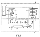
- Fig. 1 shows a combination of an information carrier 4 and a read/write unit 2.
- This combination comprises first transmitting means 9 for transmitting data from the read/write unit 2 to the information carrier 4, and second transmitting means 13 for transmitting data from the information carrier 4 to the read/write unit 2.
- the transmitting means 9 comprise a send oscillator 8 whose output is connected to the input of a send amplifier 10.
- a send coil 12 is connected to the output of the send amplifier 10.
- the send amplifier 10 can be switched on and off controlled by a microprocessor 6 through a data output of the microprocessor.
- the second transmitting means 13 inside the read/write unit 2 comprise a receive oscillator 16 whose input is connected to a receive coil 18.
- An output of the receive oscillator 16 is connected to the detector 14 for detecting amplitude variation of the receive oscillator 16.
- the output of detector 14 is connected to a data input of microprocessor 6.
- This microprocessor also has an additional data input 7.
- Microprocessor 6 is of a customary type, for example, Philips 80 C 51; it may comprise an equally prior art program memory, for example, EPROM Signetics 27 C 256 and a prior art RAM memory, for example, a 256 kbit SRAM Toshiba TC 55257 APL-12.
- the section of the first transmitting means 9 located inside the information carrier 4 comprises a receive coil 20, a diode 22, a capacitor 24, a zener diode 26 and a resistor 28.
- One side of the receive coil is connected to the anode of diode 22 whose cathode is connected to one side of capacitor 24, to the cathode of zener diode 26 and to one side of resistor 28.
- the other side of resistor 28 forms the output of the receiving section of the transmitting means inside the information carrier. This output is connected on one side to the input/output 39 of memory circuit 38 fed by a small battery 37 and on the other side to the input of the receiving section of the second transmitting means 13 inside the information carrier.
- the send section of the second transmitting means 13 comprises a parallel circuit formed by a send coil 34 and a capacitor 36. One side of this parallel circuit is connected to the common reference voltage, the other side of this parallel circuit is also connected to the common reference voltage through the main current path of a transistor 32. One side of a resistor 30 is connected to the base of transistor 32, the other side forming the input of the send section of the second transmitting means 13.
- the exchange of information between information carrier 4 and read/write unit 2 takes place as follows. As long as the read/write unit 2 does not detect the presence of an information carrier, send coil 12 of the read/write unit 2 does not radiate energy. Consequently the electronic circuit of information carrier 4 is not supplied with energy and all the points in this circuit are at quiescent potential. This means that the base of transistor 32 has the same potential as the emitter of transistor 32. So this transistor is in a non-conductive state. If the information carrier 4 is placed at the read/write location of the read/write unit 2, an inductive coupling will be effected between the receive coil 18 and send coil 34. The parallel circuit of send coil 34 and capacitor 36 forms an absorption circuit for the frequency of the receive oscillator 16 (for example, 7 MHz).
- the data transfer can now be effected controlled by the microprocessor 6.
- the send oscillator 8 (having a send frequency of e.g. 3 MHz) is connected to send coil 12 through send amplifier 10. This causes a voltage to be induced in receive coil 20, so that capacitor 24 is charged across diode 22. The voltage across capacitor 24 is stabilized by zener diode 26.
- the voltage at the junction between the cathode of zener diode 26 and resistor 28 now has the logic value "high”.
- Resistor 28 has been installed to enable the junction between resistor 28 and zener diode 26 to assume the logic value "high", while the input/output 39 of memory 38 may have the logic value "low”.
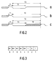
- FIG. 2 shows three time diagrams illustrating the voltage variations on input/output 39 of memory 38.
- Each of the diagrams a, b and c shows the voltage variation in a time slot with which a bit can be written in the memory 38 or read out from it respectively.
- the time slot is formed by the sum of the time intervals T1 and T3.
- Diagram a shows the voltage variation necessary for writing a 1 bit value in the memory
- diagram b shows the voltage variation necessary for writing a 0 bit value in the memory
- diagram c shows the voltage variation necessary for reading a bit from the memory.
- the memory to be writable it is first to be brought into the writing state and for the memory to be readable it is first to be brought into the reading state. This is effected by means of a command word which will be further described with reference to Fig. 3. It is assumed that the memory has already been brought into the writing state.
- a writing cycle is initiated by presenting a high-to-low transition on the input to the memory.
- the memory is now arranged so that it writes the logic value present at input/output 39 at an instant 35 ⁇ s after the high-to-low transition. Because a certain spread may occur in the above-mentioned value of 35 ⁇ s, the desired logic value is to be present on the input/output no later than after 15 ⁇ s and be maintained there till 60 ⁇ s have passed.
- T2 corresponds to 15 ⁇ s and T3 to 60 ⁇ s. From diagram a it appears that at the writing instant of 35 ⁇ s the logic value on the input/output is high so that diagram a represents the writing of a 1 bit value. From diagram b it appears that at the writing instant the logic value is low so that diagram b represents the writing of a 0 bit value.
- the memory In order to be in a position to read a bit from the memory, the memory is first to be brought into the reading state. It is assumed that this is the case.
- the reading of a bit from the memory is introduced by a high-to-low transition of input/output 39. Because the memory is in the reading state, input/output 39 shows the bit value of the memory location concerned during an interval ranging from 2 ⁇ s after the high-to-low transition to 15 ⁇ s after the high-to-low transition (interval T4). After the interval T4, the presence of this bit value has become uncertain.
- Memory 38 is used in the following manner. In order to bring the memory into a known state, first 264 zeroes are written in the memory. (The voltage variation shown in diagram b is thus repeated 264 times on input/output 39 of memory 38). Any additional zeroes to be written in the memory are discarded by the memory. The memory can now be brought into the writing or reading state by applying a defined command word to the memory.
- Fig. 3 shows the structure of this command word.
- Each command word contains 8 bits, the three first bits being formed by a 1, a 0 and a 0 in this order.
- the subsequent five bits are all to be 1's.
- one or more of these five bits are to be 0.
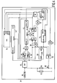
- Fig. 4 gives a more detailed representation of memory circuit 38.
- the memory circuit comprises a 256-bit shift register 42 having a serial input, a serial output and a clock input which is activated by a descending edge.
- To the serial input of shift register 42 is connected the output of OR gate 44.
- One input of OR gate 44 is connected to the output of an AND gate 46, the other input of OR gate 44 being connected to the output of an AND gate 48.
- the serial output of shift register 42 is connected, on one side, to either of the two inputs of AND gate 46 and, on the other side, to the input of inverter 76.
- the clock input of shift register 42 is connected to the output of an OR gate 50.
- One input of OR gate 50 is connected to the output of AND gate 52, the other input of OR gate 50 being connected to the output of an AND gate 54.
- the memory circuit 38 further includes an 8-bit shift register 62 having a serial input, a parallel output and a clock input which is activated by a descending edge.
- the parallel input of decoding logic 64 is connected to the parallel output of shift register 62.
- This decoding logic 64 furthermore has a 1-bit reset input, a 1-bit initialization input, a 1-bit read output and a 1-bit write output.
- Input buffer 60 is merely used for bringing the input pulses into the proper form.
- the output of buffer 60 is connected to the serial input of shift register 62, an input of AND gate 48 and the clock input of a one-shot multivibrator 68.
- This clock input is activated by a descending edge of the signal supplied thereto.
- This multivibrator 68 produces a pulse having a duration of about 35 ⁇ s on its output in response to a descending edge on its clock input.
- the output of the multivibrator 68 is connected to the clock input of shift register 62, the input of an inverter 56, the first of three inputs of AND gate 54, the clock input of counter 70 and to the second of three inputs of an AND gate 78.
- the 8-bit counter 70 has an overflow output connected to the set input of a flip-flop 72 and to the reset input of decoding logic 64.
- the output of flip-flop 72 is connected to the reset input of counter 70 and the input of an inverter 58, whose output is connected to the second of three inputs of AND gate 54.
- the reset input of flip-flop 72 is connected to an output of an OR gate 74.
- the write output of decoding logic 64 is connected to an input of AND gate 48, a third input of AND gate 54 and to a first of three inputs of OR gate 74.
- the read output of decoding logic 64 is connected to an input of AND gate 46, an input of AND gate 52 and to the first of three inputs of AND gate 78.
- the initialization output of decoding logic 64 is connected to the third input of OR gate 74.
- inverter 76 is connected to the third input of AND gate 78.
- the output of this AND gate is connected to the gate of field effect transistor 80, whose first main electrode is connected to data input 39 through a resistor 84 of, for example, 100 ⁇ and whose second main electrode is connected to the common reference voltage.
- resistor 84 is connected to data input 39.
- resistor 82 which has a value of, for example, 500 ⁇ . The other side of this resistor is connected to the common reference voltage.
- flip-flop 72 is of the asymmetric type, which is to say that the output is high when the supply voltage is switched on. Consequently, the 8-bit counter 70 is initially kept in the reset state.
- a complete memory cycle consists of an initialization part during which the memory is brought to a prior-art state, a command word as described with reference to Fig. 3, and a read or write sequence of 256 bits.
- the initialization part consists of supplying 264 time slots for writing 0-bit values (write-zero-time slot) to the data input 39.
- one-shot multivibrator 68 With the first descending edge (thus at the end of time interval T1 in Fig. 2b) one-shot multivibrator 68 generates a 35 ⁇ s pulse. Due to the descending edge of this pulse the clock input of shift register 62 is activated so that a 0-bit value is written in the shift register (Counter 70 does not change its count because the reset input is high).
- the data in the shift register 42 are shifted by one location. It is assumed that a 0-bit value, i.e. logic value "low", appears on the serial output of this shift register. This low value is inverted to a high value by the inverter 76. All three inputs of AND gate 78 are high now: the first input is connected to the read output of decoding logic 64, to the second input is applied the 35 ⁇ s pulse multivibrator 68 and the third input is connected to the output of inverter 76. Consequently, the output of AND gate 78 will be high, so that field effect transistor 80 is rendered conductive. The result is that the data input 39 is connected to the common reference voltage through the low resistor 14. As a result, the base of transistor 32 ( cf . Fig. 1) is kept low, so that the resonance circuit (34, 36) is no longer short-circuited. This situation is detected by detector 14 which delivers the thus detected 0-bit to microprocessor 6.
- a write command word is applied to shift register 62, i.e. a sequence of 8 bits of which the first bit is a 1, the next two 0's and all further bits are 1's.
- the write output of decoding logic 64 becomes high. (The two other inputs remain low.)
- This high value is passed on through OR gate 74 to the reset input of flip-flop 72, so that its output becomes low and counter 70 is moved to the counting state.
- This low output value is likewise made high by the inverter 58 and supplied to an input of AND gate 54.
- the high write signal of decoding logic 64 is then applied to an input of AND gate 48 and to an input of AND gate 54.
- AND gate 48 is connected to data input 39. If a 1-bit value is available on data input 39 at the write instant, the output of AND gate 48 will also present the value of 1 and this value will be applied to the input of shift register 42 through OR gate 44; if at that moment a 0-bit value is present on data input 39, one of the inputs of AND gate 48 will be low so that the output of this gate will also be low. This low value will then be applied to shift register 42.
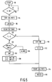
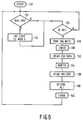
- FIG. 5 illustrates the course of the process in the read/write unit when an information carrier is used as a hotel key.
- the blocks in this flow chart have the following connotations:
- the information carrier When the information carrier is used as a key for a hotel room or bungalow in a holiday park, the information carrier (i.e. the key) is inserted into a read/write unit outside the door or the bungalow. After the access cycle has been started (90) it is verified whether there is a key present at the read/write location (92). If there is, the reading of the key is initialized by the transmission of 264 write-0 time slots (94) to the key. After the memory in the key is brought to a known state in this manner, the read command word is transmitted to the key (96). Then the read/write unit transmits 256 read time slots to the key and reads the relevant bits from the time slots in the key memory (98).
- the read/write unit In the 256 bit sequence there are a number of bits forming the access codeword.
- the read/write unit is to adopt this codeword so as to calculate therefrom new codewords at a later stage, for example, by adding unity thereto.
- a bit F In order to indicate that the key has not yet been inserted into the relevant read/write unit before, there is a bit F, a flag, representing this situation with the 1-bit value.
- the processor is thus to verify whether the flag has the 0 value (100). If not, the key has been inserted into the read/write unit for the first time.
- the access codeword is taken over by the memory of the read/write unit (110) after which the flag is set to 0 (112). Then the thus modified (F from 1 to 0) bit sequence is again written back to the key memory and access is given to the room.
- the access codeword read out from the key is compared with the access codeword present in the memory of the read/write unit (102). If these words do not match, an alarm signal can be given (104). If they do match, a new access codeword is calculated on the basis of the access codeword present (106). For this purpose, a simple algorithm may be used, for example, adding unity to the number represented by the bit combination of the codeword. Alternatively, more intricate algorithms are possible.
- the newly calculated access codeword is now stored both in the bit sequence intended for the key and in the memory of the read/write unit (108). Finally, the bit sequence containing the new access codeword is written in the key memory (114) and access is given to the room (116).
- the flow chart represented in Fig. 6 illustrates the course of the process in a read/write unit used as mail/message indicator.
- the blocks in this flow chart have the following connotations:
- this unit may be used as a mail/message indicator, for example, in a hotel or holiday park. Through the additional data input there may be stored in the memory of the read/write unit for each room whether there is any mail or message.
- the memory in the information carrier thereto has a unique identification code, for example, the room number. If there is any mail for that specific room, this will be notified to the first memory field of the read/write unit (122 or 124) at a memory address matching the identification code. If a hotel guest returns to the hotel, he places his information carrier at the read/write location where it is read out by the read/write unit (126).
- the reading of the key is initialized by sending 264 write-0 time slots to the key (128). Once the memory in the key has been moved to a known state in this manner, the command word for reading is sent to the key (130). Then the read/write unit sends 256 read time slots to the key and reads from each time slot the relevant bit from the key memory (132). After the 256-bit bit sequence from the information carrier has been read out, the read/write unit selects the identification code (134). This identification code forms the address of the location in the first memory field from which the indication code is to be read out. This code is decoded. The result may be that there is no message at all. In that case a light is activated representing this situation. For example, if a telefax message has arrived, a different light is activated representing that situation. Thus, after the hotel guest has been informed of this message, the indication code is erased and the process returns to the starting point.
Landscapes
- Engineering & Computer Science (AREA)
- Theoretical Computer Science (AREA)
- Physics & Mathematics (AREA)
- General Physics & Mathematics (AREA)
- Computer Vision & Pattern Recognition (AREA)
- Artificial Intelligence (AREA)
- Microelectronics & Electronic Packaging (AREA)
- Computer Hardware Design (AREA)
- Computer Networks & Wireless Communication (AREA)
- Mobile Radio Communication Systems (AREA)
- Read Only Memory (AREA)
- Near-Field Transmission Systems (AREA)
- Management, Administration, Business Operations System, And Electronic Commerce (AREA)
Applications Claiming Priority (2)
| Application Number | Priority Date | Filing Date | Title |
|---|---|---|---|
| NL9001930A NL9001930A (nl) | 1990-09-03 | 1990-09-03 | Stelsel voor informatie-uitwisseling, met een informatiedrager en een lees- en schrijfeenheid. |
| NL9001930 | 1990-09-03 |
Publications (3)
| Publication Number | Publication Date |
|---|---|
| EP0474286A2 true EP0474286A2 (de) | 1992-03-11 |
| EP0474286A3 EP0474286A3 (de) | 1994-04-20 |
| EP0474286B1 EP0474286B1 (de) | 1996-11-06 |
Family
ID=19857616
Family Applications (1)
| Application Number | Title | Priority Date | Filing Date |
|---|---|---|---|
| EP91202171A Expired - Lifetime EP0474286B1 (de) | 1990-09-03 | 1991-08-27 | Informationsaustauschsystem mit einem Informationsträger und einer Lese- und Schreibeinheit |
Country Status (7)
| Country | Link |
|---|---|
| US (1) | US5321395A (de) |
| EP (1) | EP0474286B1 (de) |
| JP (1) | JP3126758B2 (de) |
| KR (1) | KR100211623B1 (de) |
| DE (1) | DE69123021T2 (de) |
| NL (1) | NL9001930A (de) |
| NO (1) | NO913413L (de) |
Families Citing this family (18)
| Publication number | Priority date | Publication date | Assignee | Title |
|---|---|---|---|---|
| US6137476A (en) * | 1994-08-25 | 2000-10-24 | International Business Machines Corp. | Data mouse |
| JPH08138018A (ja) * | 1994-11-10 | 1996-05-31 | Rikagaku Kenkyusho | データ・キャリア・システム |
| JP3239683B2 (ja) * | 1995-05-11 | 2001-12-17 | 株式会社セガ | 画像処理装置および画像処理方法 |
| US5936542A (en) * | 1995-09-11 | 1999-08-10 | Nomadix, Llc | Convention ID badge system |
| JP3565967B2 (ja) * | 1995-12-21 | 2004-09-15 | 富士通株式会社 | Icカード読み取り/書き込み装置及びicカードシステム |
| US6194992B1 (en) | 1997-04-24 | 2001-02-27 | Nomadix, Llc | Mobile web |
| US6100788A (en) * | 1997-12-29 | 2000-08-08 | Storage Technology Corporation | Multifunctional electromagnetic transponder device and method for performing same |
| US5949342A (en) * | 1997-12-31 | 1999-09-07 | Storage Technology Corporation | Shock sensing and reporting device |
| US8713641B1 (en) | 1998-12-08 | 2014-04-29 | Nomadix, Inc. | Systems and methods for authorizing, authenticating and accounting users having transparent computer access to a network using a gateway device |
| US7194554B1 (en) | 1998-12-08 | 2007-03-20 | Nomadix, Inc. | Systems and methods for providing dynamic network authorization authentication and accounting |
| US8266266B2 (en) | 1998-12-08 | 2012-09-11 | Nomadix, Inc. | Systems and methods for providing dynamic network authorization, authentication and accounting |
| US6546133B1 (en) | 1999-09-08 | 2003-04-08 | Ge Capital Commercial Finance, Inc. | Methods and apparatus for print scraping |
| US8271321B1 (en) * | 2000-06-05 | 2012-09-18 | Buildinglink.com, LLC | Apparatus and method for providing building management information |
| JP2002230214A (ja) * | 2001-02-01 | 2002-08-16 | Fujitsu Ltd | 情報の提供方法および印刷システムならびにイベントシステム |
| DE10325399A1 (de) * | 2003-05-28 | 2004-12-30 | Atmel Germany Gmbh | Schaltungsanordnung zur Phasenmodulation für rückstreubasierte Transporder |
| US20050261970A1 (en) * | 2004-05-21 | 2005-11-24 | Wayport, Inc. | Method for providing wireless services |
| EP2549443A3 (de) | 2004-09-16 | 2013-05-29 | Fortress GB Ltd. | Offline-/Online-Zugangssteuerungssystem mit Rückkauffunktionalität zur Steuerung des Zugangs auf einen abgeschlossenen Bereich mit einem massenbesuchten Ereignis |
| US8261327B2 (en) | 2007-07-12 | 2012-09-04 | Wayport, Inc. | Device-specific authorization at distributed locations |
Family Cites Families (9)
| Publication number | Priority date | Publication date | Assignee | Title |
|---|---|---|---|---|
| US4353064A (en) * | 1981-01-14 | 1982-10-05 | Honeywell Inc. | Battery operated access control card |
| CA1240056A (en) * | 1983-12-06 | 1988-08-02 | Adrian Lewis | Tokens and token handling devices |
| JPS6141262A (ja) * | 1984-07-31 | 1986-02-27 | Omron Tateisi Electronics Co | 音声記録可能なカ−ド |
| US4605844A (en) * | 1985-02-11 | 1986-08-12 | At&T Technologies, Inc. | Computerized transaction card with inductive data transfer |
| GB8509135D0 (en) * | 1985-04-10 | 1985-05-15 | Gen Electric Co Plc | Transaction system |
| JPS6274189A (ja) * | 1985-09-27 | 1987-04-04 | Toshiba Corp | 情報媒体 |
| IL82025A (en) * | 1987-03-27 | 1993-07-08 | Galil Electro Ltd | Electronic data communications system |
| EP0289830A3 (de) * | 1987-05-08 | 1991-09-11 | Baumer Electric Ag | Identifikationssystem mit einer Mehrzahl von Vorrichtungen zum Schreiben, Lesen und Erkennen eines Codes sowie eine Vielzahl von Codeträgern und Verfahren dazu |
| EP0309201B1 (de) * | 1987-09-22 | 1993-05-26 | Hitachi Maxell Ltd. | Übertragungsverfahren und -System für kontaktlose I.S.-Karten |
-
1990
- 1990-09-03 NL NL9001930A patent/NL9001930A/nl not_active Application Discontinuation
-
1991
- 1991-08-27 DE DE69123021T patent/DE69123021T2/de not_active Expired - Fee Related
- 1991-08-27 EP EP91202171A patent/EP0474286B1/de not_active Expired - Lifetime
- 1991-08-29 US US07/751,288 patent/US5321395A/en not_active Expired - Fee Related
- 1991-08-30 NO NO91913413A patent/NO913413L/no unknown
- 1991-09-02 KR KR1019910015229A patent/KR100211623B1/ko not_active Expired - Fee Related
- 1991-09-03 JP JP03222718A patent/JP3126758B2/ja not_active Expired - Fee Related
Also Published As
| Publication number | Publication date |
|---|---|
| EP0474286A3 (de) | 1994-04-20 |
| DE69123021T2 (de) | 1997-05-15 |
| NL9001930A (nl) | 1992-04-01 |
| DE69123021D1 (de) | 1996-12-12 |
| KR920006864A (ko) | 1992-04-28 |
| US5321395A (en) | 1994-06-14 |
| JP3126758B2 (ja) | 2001-01-22 |
| NO913413D0 (no) | 1991-08-30 |
| EP0474286B1 (de) | 1996-11-06 |
| JPH04245587A (ja) | 1992-09-02 |
| KR100211623B1 (ko) | 1999-08-02 |
| NO913413L (no) | 1992-03-04 |
Similar Documents
| Publication | Publication Date | Title |
|---|---|---|
| EP0474286A2 (de) | Informationsaustauschsystem mit einem Informationsträger und einer Lese- und Schreibeinheit | |
| EP0040544B1 (de) | Kodierte Informationsanordnung | |
| US4514731A (en) | Coded information arrangement | |
| USRE35336E (en) | Self-contained programmable terminal for security systems | |
| US4120452A (en) | Automatic vending system | |
| EP0171433B1 (de) | Identifikationssystem und transponder | |
| JPS58145263A (ja) | 伝送器/応答器システム | |
| EP0615645B1 (de) | Elektronisches identifikationsetikett für einen mehrspeicher. | |
| US4473825A (en) | Electronic identification system with power input-output interlock and increased capabilities | |
| US4004097A (en) | Automatic meter reading device | |
| JP2519237B2 (ja) | 物体同定システム | |
| USRE29450E (en) | Machine operating condition monitoring system | |
| US5142556A (en) | Data transfer system and method of transferring data | |
| EP0022458B1 (de) | Hierarchisches Datenverarbeitungssystem für eine Eingangskontrolle | |
| EP0082690B1 (de) | Sender-Antwortbakensystem | |
| KR100689048B1 (ko) | 코히어런트 신호 간섭 감소를 위한 부호화/복호화 시스템 | |
| US4273996A (en) | Sequential card reader system | |
| US5432853A (en) | Digital signal processing system | |
| JP4697695B2 (ja) | 非接触式電子ラベル共通メッセージ同時書き込み方法 | |
| US3234533A (en) | System for displaying and registering signals | |
| AU2826689A (en) | Apparatus and method for identification of message initiation in a process control network | |
| JP2930972B2 (ja) | 読取器及びトランスポンダー | |
| US4055835A (en) | Line-seizing apparatus | |
| US3286235A (en) | Information storage system | |
| JPH05346978A (ja) | データキャリア及び識別システム |
Legal Events
| Date | Code | Title | Description |
|---|---|---|---|
| PUAI | Public reference made under article 153(3) epc to a published international application that has entered the european phase |
Free format text: ORIGINAL CODE: 0009012 |
|
| AK | Designated contracting states |
Kind code of ref document: A2 Designated state(s): DE FR GB NL |
|
| PUAL | Search report despatched |
Free format text: ORIGINAL CODE: 0009013 |
|
| AK | Designated contracting states |
Kind code of ref document: A3 Designated state(s): DE FR GB NL |
|
| 17P | Request for examination filed |
Effective date: 19941019 |
|
| 17Q | First examination report despatched |
Effective date: 19950529 |
|
| GRAG | Despatch of communication of intention to grant |
Free format text: ORIGINAL CODE: EPIDOS AGRA |
|
| GRAH | Despatch of communication of intention to grant a patent |
Free format text: ORIGINAL CODE: EPIDOS IGRA |
|
| GRAH | Despatch of communication of intention to grant a patent |
Free format text: ORIGINAL CODE: EPIDOS IGRA |
|
| GRAA | (expected) grant |
Free format text: ORIGINAL CODE: 0009210 |
|
| AK | Designated contracting states |
Kind code of ref document: B1 Designated state(s): DE FR GB NL |
|
| REF | Corresponds to: |
Ref document number: 69123021 Country of ref document: DE Date of ref document: 19961212 |
|
| ET | Fr: translation filed | ||
| PLBE | No opposition filed within time limit |
Free format text: ORIGINAL CODE: 0009261 |
|
| STAA | Information on the status of an ep patent application or granted ep patent |
Free format text: STATUS: NO OPPOSITION FILED WITHIN TIME LIMIT |
|
| 26N | No opposition filed | ||
| NLT1 | Nl: modifications of names registered in virtue of documents presented to the patent office pursuant to art. 16 a, paragraph 1 |
Owner name: KONINKLIJKE PHILIPS ELECTRONICS N.V. |
|
| REG | Reference to a national code |
Ref country code: FR Ref legal event code: CD |
|
| PGFP | Annual fee paid to national office [announced via postgrant information from national office to epo] |
Ref country code: NL Payment date: 20010831 Year of fee payment: 11 |
|
| REG | Reference to a national code |
Ref country code: GB Ref legal event code: IF02 |
|
| REG | Reference to a national code |
Ref country code: FR Ref legal event code: D6 |
|
| REG | Reference to a national code |
Ref country code: GB Ref legal event code: 746 Effective date: 20021231 |
|
| PG25 | Lapsed in a contracting state [announced via postgrant information from national office to epo] |
Ref country code: NL Free format text: LAPSE BECAUSE OF NON-PAYMENT OF DUE FEES Effective date: 20030301 |
|
| NLV4 | Nl: lapsed or anulled due to non-payment of the annual fee |
Effective date: 20030301 |
|
| PGFP | Annual fee paid to national office [announced via postgrant information from national office to epo] |
Ref country code: GB Payment date: 20040826 Year of fee payment: 14 |
|
| PGFP | Annual fee paid to national office [announced via postgrant information from national office to epo] |
Ref country code: FR Payment date: 20040830 Year of fee payment: 14 |
|
| PGFP | Annual fee paid to national office [announced via postgrant information from national office to epo] |
Ref country code: DE Payment date: 20041015 Year of fee payment: 14 |
|
| PG25 | Lapsed in a contracting state [announced via postgrant information from national office to epo] |
Ref country code: GB Free format text: LAPSE BECAUSE OF NON-PAYMENT OF DUE FEES Effective date: 20050827 |
|
| PG25 | Lapsed in a contracting state [announced via postgrant information from national office to epo] |
Ref country code: DE Free format text: LAPSE BECAUSE OF NON-PAYMENT OF DUE FEES Effective date: 20060301 |
|
| GBPC | Gb: european patent ceased through non-payment of renewal fee |
Effective date: 20050827 |
|
| PG25 | Lapsed in a contracting state [announced via postgrant information from national office to epo] |
Ref country code: FR Free format text: LAPSE BECAUSE OF NON-PAYMENT OF DUE FEES Effective date: 20060428 |
|
| REG | Reference to a national code |
Ref country code: FR Ref legal event code: ST Effective date: 20060428 |