EP0474156B1 - Verfahren zum überprüfen der Eingänge eines Mikroprozessors - Google Patents
Verfahren zum überprüfen der Eingänge eines Mikroprozessors Download PDFInfo
- Publication number
- EP0474156B1 EP0474156B1 EP91114733A EP91114733A EP0474156B1 EP 0474156 B1 EP0474156 B1 EP 0474156B1 EP 91114733 A EP91114733 A EP 91114733A EP 91114733 A EP91114733 A EP 91114733A EP 0474156 B1 EP0474156 B1 EP 0474156B1
- Authority
- EP
- European Patent Office
- Prior art keywords
- input
- voltage
- reactance
- microprocessor
- timing member
- Prior art date
- Legal status (The legal status is an assumption and is not a legal conclusion. Google has not performed a legal analysis and makes no representation as to the accuracy of the status listed.)
- Expired - Lifetime
Links
Images
Classifications
-
- G—PHYSICS
- G06—COMPUTING OR CALCULATING; COUNTING
- G06F—ELECTRIC DIGITAL DATA PROCESSING
- G06F11/00—Error detection; Error correction; Monitoring
- G06F11/07—Responding to the occurrence of a fault, e.g. fault tolerance
- G06F11/0796—Safety measures, i.e. ensuring safe condition in the event of error, e.g. for controlling element
-
- F—MECHANICAL ENGINEERING; LIGHTING; HEATING; WEAPONS; BLASTING
- F23—COMBUSTION APPARATUS; COMBUSTION PROCESSES
- F23N—REGULATING OR CONTROLLING COMBUSTION
- F23N5/00—Systems for controlling combustion
- F23N5/20—Systems for controlling combustion with a time program acting through electrical means, e.g. using time-delay relays
- F23N5/203—Systems for controlling combustion with a time program acting through electrical means, e.g. using time-delay relays using electronic means
-
- G—PHYSICS
- G06—COMPUTING OR CALCULATING; COUNTING
- G06F—ELECTRIC DIGITAL DATA PROCESSING
- G06F11/00—Error detection; Error correction; Monitoring
- G06F11/07—Responding to the occurrence of a fault, e.g. fault tolerance
- G06F11/0703—Error or fault processing not based on redundancy, i.e. by taking additional measures to deal with the error or fault not making use of redundancy in operation, in hardware, or in data representation
- G06F11/0751—Error or fault detection not based on redundancy
- G06F11/0754—Error or fault detection not based on redundancy by exceeding limits
- G06F11/0757—Error or fault detection not based on redundancy by exceeding limits by exceeding a time limit, i.e. time-out, e.g. watchdogs
-
- F—MECHANICAL ENGINEERING; LIGHTING; HEATING; WEAPONS; BLASTING
- F23—COMBUSTION APPARATUS; COMBUSTION PROCESSES
- F23N—REGULATING OR CONTROLLING COMBUSTION
- F23N2223/00—Signal processing; Details thereof
- F23N2223/08—Microprocessor; Microcomputer
-
- F—MECHANICAL ENGINEERING; LIGHTING; HEATING; WEAPONS; BLASTING
- F23—COMBUSTION APPARATUS; COMBUSTION PROCESSES
- F23N—REGULATING OR CONTROLLING COMBUSTION
- F23N2231/00—Fail safe
- F23N2231/10—Fail safe for component failures
Definitions
- the invention relates to a method for checking the correct wiring and programming of the inputs of a microprocessor in a control unit, in particular a burner control unit.
- Control units of this type are subject to various safety conditions. For example, the ignition of the flame may only be initiated if any residual gases have previously been flushed out of the combustion chamber. The main gas valve may only open if it is ensured that the pilot light burns. These conditions require that the corresponding sensors work reliably and intrinsically safe on the one hand and that the microprocessor is correctly wired and programmed on the other hand. Under no circumstances should the correct operation of any assembly, such as the blower or the ignition device, be faked if there is actually a fault. Intrinsically safe sensors and monitoring circuits are known in many forms. Devices are also known for monitoring the correct functioning of electronic controls, with which the wiring of their outputs can also be checked (see eee news from September 17, 1985, p. 8, right column).
- GB-A 2 159 982 describes a programmable logic controller with a circuit which is used either as an input circuit for receiving the signals of an input device or as an output circuit for delivering control signals to a load.
- the object of the invention is also to include the microprocessor controlling the program sequence in the self-monitoring.
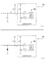
- the microprocessor 10 has a number of inputs E, only one of which is shown. This connection is connected to ground via a timing element.
- this timing element consists of a resistor R1 and a capacitor C.
- a resistor R2 connects the input to an operating voltage terminal V c . If there is no such internal resistor R2, an external resistor R2 'can instead be used to supply the operating voltage V c to the input E.
- the microprocessor 10 also contains an I / O selection logic, via which the input E can optionally be configured as an output by the program. In this case, the amplifier V1 turns on the transistor T1 and thus connects the input E to ground. There is therefore a signal (O) at the input.
- input E is effective as an input, the input signal fed to it passes through amplifier V2 to the relevant microprocessor circuits. The input is checked as follows:
- the input E is configured as an output by the selection logic 12.
- the transistor T1 connects the input E to ground. If the capacitor C was previously charged, it discharges through the resistor R1 and the transistor T1. A logic level O is thus at input E. After a predetermined period of time, which corresponds, for example, to ten times the time constant C x R1, it can be assumed that the capacitor is completely discharged. After this, the connection E is configured again as an input via the selection logic 12.
- the voltage at input E is measured. Since capacitor C is discharged, it must have the value O. The measurement should be carried out within a period of time t ⁇ 0.1 RC. The measured value is saved. Since the input E is separated from the ground potential by the now blocked transistor T1, the capacitor C charges up from the operating voltage V c via the resistors R2 and R1. After a period of time that is approximately ten times the value of the time constant of this charging circuit, ie t ⁇ C x (R1 + R2), the voltage at input E is measured again. Now, if it is operating properly, it must have a value other than O, i.e. the value 1.
- a coil L serves as a reactance instead of a capacitor. This has an ohmic inherent resistance, so that the resistor R1 can be omitted.
- the resistor R1 is used in the circuit according to FIG. 1 to limit the current at the input E. If the microprocessor is short-circuit proof, the resistor R1 can also be omitted in FIG. 1.
- the test process proceeds in the same way as before described with reference to FIG. 1. First, the coil L is short-circuited via the transistor T1 when the input E is configured as an output. As soon as the reconfiguration as input has taken place, the voltage at input E is measured within a period of time t ⁇ 0.1L / R2.
Landscapes
- Engineering & Computer Science (AREA)
- Theoretical Computer Science (AREA)
- General Engineering & Computer Science (AREA)
- Quality & Reliability (AREA)
- Physics & Mathematics (AREA)
- General Physics & Mathematics (AREA)
- Chemical & Material Sciences (AREA)
- Combustion & Propulsion (AREA)
- Mechanical Engineering (AREA)
- Regulation And Control Of Combustion (AREA)
- Testing Of Short-Circuits, Discontinuities, Leakage, Or Incorrect Line Connections (AREA)
Applications Claiming Priority (2)
| Application Number | Priority Date | Filing Date | Title |
|---|---|---|---|
| DE4027950A DE4027950C1 (cg-RX-API-DMAC10.html) | 1990-09-04 | 1990-09-04 | |
| DE4027950 | 1990-09-04 |
Publications (3)
| Publication Number | Publication Date |
|---|---|
| EP0474156A2 EP0474156A2 (de) | 1992-03-11 |
| EP0474156A3 EP0474156A3 (en) | 1992-07-22 |
| EP0474156B1 true EP0474156B1 (de) | 1996-01-03 |
Family
ID=6413526
Family Applications (1)
| Application Number | Title | Priority Date | Filing Date |
|---|---|---|---|
| EP91114733A Expired - Lifetime EP0474156B1 (de) | 1990-09-04 | 1991-09-02 | Verfahren zum überprüfen der Eingänge eines Mikroprozessors |
Country Status (2)
| Country | Link |
|---|---|
| EP (1) | EP0474156B1 (cg-RX-API-DMAC10.html) |
| DE (2) | DE4027950C1 (cg-RX-API-DMAC10.html) |
Family Cites Families (2)
| Publication number | Priority date | Publication date | Assignee | Title |
|---|---|---|---|---|
| US4593380A (en) * | 1984-06-04 | 1986-06-03 | General Electric Co. | Dual function input/output for a programmable controller |
| JPH0719121B2 (ja) * | 1988-01-11 | 1995-03-06 | 三菱電機株式会社 | プログラマブルコントローラの時分割入力方法 |
-
1990
- 1990-09-04 DE DE4027950A patent/DE4027950C1/de not_active Expired - Fee Related
-
1991
- 1991-09-02 EP EP91114733A patent/EP0474156B1/de not_active Expired - Lifetime
- 1991-09-02 DE DE59107196T patent/DE59107196D1/de not_active Expired - Fee Related
Also Published As
| Publication number | Publication date |
|---|---|
| DE59107196D1 (de) | 1996-02-15 |
| EP0474156A2 (de) | 1992-03-11 |
| EP0474156A3 (en) | 1992-07-22 |
| DE4027950C1 (cg-RX-API-DMAC10.html) | 1991-12-19 |
Similar Documents
| Publication | Publication Date | Title |
|---|---|---|
| EP3171124B2 (de) | Verfahren für den betrieb einer kapazitiven sensoranordnung eines kraftfahrzeugs | |
| EP0011680A1 (de) | Prüfschaltung für die Auslösevorrichtung einer den Schutz der Insassen eines Fahrzeugs während eines Unfalles dienenden Sicherheitseinrichtung | |
| DE4029703A1 (de) | Fehler-spuergeraet fuer ein airbag-system | |
| DE19718041A1 (de) | Schaltungsanordnung und Verfahren zur Überprüfung der Kontaktierung eines Schalters oder Tasters | |
| DE3835115A1 (de) | Elektrischer verzoegerungszuender | |
| DE4027950C1 (cg-RX-API-DMAC10.html) | ||
| DE3150212C1 (de) | Schaltungsanordnung für einen Näherungsschalter | |
| DE19836734A1 (de) | Verfahren zur Funktionsprüfung eines Zündkreises eines Insassenschutzsystems sowie Prüfschaltung | |
| EP0365950A2 (de) | Schaltungsanordnung zur Einstellung des Auslösepunktes in einer induktiven Tastatur | |
| DE4033234A1 (de) | Sicherheitslichtgitter | |
| DE2647569B2 (de) | Impulsgenerator mit umschaltbarer Ausgangsfrequenz | |
| EP0729034A2 (de) | Prüfschaltung und Prüfverfahren zur Funktionsprüfung von elektronischen Schaltungen | |
| DE102021001093B4 (de) | Eingebundenes Testinstrument für Hochgeschwindigkeitsschnittstellen | |
| DE3220111C1 (de) | Überwachungseinrichtung für Näherungsschalter | |
| EP1494098B1 (de) | Steuergerät für die Sicherheitstechnik und entsprechendes Steuerungsverfahren | |
| EP4277066B1 (de) | Sicherheitsschaltvorrichtung insbesondere zum überwachten einschalten eines elektrischen und/oder elektronischen verbrauchers | |
| WO2020148321A1 (de) | Vorrichtung und verfahren zur funktionsprüfung eines antennensystems zur fremdmetallerkennung | |
| WO2020148324A1 (de) | Vorrichtung und verfahren zur funktionsprüfung eines antennensystems zur fremdmetallerkennung | |
| DE102004063708B4 (de) | Schaltung zur Spannungsbegrenzung | |
| DE1951438B2 (de) | Einrichtung zur gleichzeitigen Überwachung mehrerer Flammen | |
| DE2006757C3 (de) | Elektrische Schaltungsanordnung zur stufenlosen Veränderung der Nachstellzeitkonstanten eines Reglers mit nachgebender Rückführung | |
| DE19922818A1 (de) | Verfahren zur Überprüfung einer Auswerteschaltung | |
| DE3403788C2 (cg-RX-API-DMAC10.html) | ||
| EP1388869A2 (de) | Prüfschaltung für eine Zündspule und Verfahren zum Prüfen einer Zündspule | |
| DD143130A1 (de) | Gesteuerte abschneidefunkenstrecke |
Legal Events
| Date | Code | Title | Description |
|---|---|---|---|
| PUAI | Public reference made under article 153(3) epc to a published international application that has entered the european phase |
Free format text: ORIGINAL CODE: 0009012 |
|
| AK | Designated contracting states |
Kind code of ref document: A2 Designated state(s): DE IT NL |
|
| PUAL | Search report despatched |
Free format text: ORIGINAL CODE: 0009013 |
|
| AK | Designated contracting states |
Kind code of ref document: A3 Designated state(s): DE IT NL |
|
| 17P | Request for examination filed |
Effective date: 19930120 |
|
| 17Q | First examination report despatched |
Effective date: 19941216 |
|
| GRAA | (expected) grant |
Free format text: ORIGINAL CODE: 0009210 |
|
| AK | Designated contracting states |
Kind code of ref document: B1 Designated state(s): DE IT NL |
|
| REF | Corresponds to: |
Ref document number: 59107196 Country of ref document: DE Date of ref document: 19960215 |
|
| ITF | It: translation for a ep patent filed | ||
| PGFP | Annual fee paid to national office [announced via postgrant information from national office to epo] |
Ref country code: DE Payment date: 19960617 Year of fee payment: 6 |
|
| PGFP | Annual fee paid to national office [announced via postgrant information from national office to epo] |
Ref country code: NL Payment date: 19960820 Year of fee payment: 6 |
|
| PLBE | No opposition filed within time limit |
Free format text: ORIGINAL CODE: 0009261 |
|
| STAA | Information on the status of an ep patent application or granted ep patent |
Free format text: STATUS: NO OPPOSITION FILED WITHIN TIME LIMIT |
|
| 26N | No opposition filed | ||
| PG25 | Lapsed in a contracting state [announced via postgrant information from national office to epo] |
Ref country code: NL Free format text: LAPSE BECAUSE OF NON-PAYMENT OF DUE FEES Effective date: 19980401 |
|
| NLV4 | Nl: lapsed or anulled due to non-payment of the annual fee |
Effective date: 19980401 |
|
| PG25 | Lapsed in a contracting state [announced via postgrant information from national office to epo] |
Ref country code: DE Free format text: LAPSE BECAUSE OF NON-PAYMENT OF DUE FEES Effective date: 19980603 |
|
| PG25 | Lapsed in a contracting state [announced via postgrant information from national office to epo] |
Ref country code: IT Free format text: LAPSE BECAUSE OF NON-PAYMENT OF DUE FEES;WARNING: LAPSES OF ITALIAN PATENTS WITH EFFECTIVE DATE BEFORE 2007 MAY HAVE OCCURRED AT ANY TIME BEFORE 2007. THE CORRECT EFFECTIVE DATE MAY BE DIFFERENT FROM THE ONE RECORDED. Effective date: 20050902 |