EP0471684B1 - Schaltung und verfahren zum messen einer die kapazitäts-spannungs-charakteristik eines kapazitiven elementes beeinflussenden grösse - Google Patents
Schaltung und verfahren zum messen einer die kapazitäts-spannungs-charakteristik eines kapazitiven elementes beeinflussenden grösse Download PDFInfo
- Publication number
- EP0471684B1 EP0471684B1 EP90906167A EP90906167A EP0471684B1 EP 0471684 B1 EP0471684 B1 EP 0471684B1 EP 90906167 A EP90906167 A EP 90906167A EP 90906167 A EP90906167 A EP 90906167A EP 0471684 B1 EP0471684 B1 EP 0471684B1
- Authority
- EP
- European Patent Office
- Prior art keywords
- voltage
- capacitive
- capacitance
- semiconductor element
- concentration
- Prior art date
- Legal status (The legal status is an assumption and is not a legal conclusion. Google has not performed a legal analysis and makes no representation as to the accuracy of the status listed.)
- Expired - Lifetime
Links
Images


Classifications
-
- G—PHYSICS
- G01—MEASURING; TESTING
- G01D—MEASURING NOT SPECIALLY ADAPTED FOR A SPECIFIC VARIABLE; ARRANGEMENTS FOR MEASURING TWO OR MORE VARIABLES NOT COVERED IN A SINGLE OTHER SUBCLASS; TARIFF METERING APPARATUS; MEASURING OR TESTING NOT OTHERWISE PROVIDED FOR
- G01D5/00—Mechanical means for transferring the output of a sensing member; Means for converting the output of a sensing member to another variable where the form or nature of the sensing member does not constrain the means for converting; Transducers not specially adapted for a specific variable
- G01D5/12—Mechanical means for transferring the output of a sensing member; Means for converting the output of a sensing member to another variable where the form or nature of the sensing member does not constrain the means for converting; Transducers not specially adapted for a specific variable using electric or magnetic means
- G01D5/14—Mechanical means for transferring the output of a sensing member; Means for converting the output of a sensing member to another variable where the form or nature of the sensing member does not constrain the means for converting; Transducers not specially adapted for a specific variable using electric or magnetic means influencing the magnitude of a current or voltage
- G01D5/24—Mechanical means for transferring the output of a sensing member; Means for converting the output of a sensing member to another variable where the form or nature of the sensing member does not constrain the means for converting; Transducers not specially adapted for a specific variable using electric or magnetic means influencing the magnitude of a current or voltage by varying capacitance
- G01D5/2403—Mechanical means for transferring the output of a sensing member; Means for converting the output of a sensing member to another variable where the form or nature of the sensing member does not constrain the means for converting; Transducers not specially adapted for a specific variable using electric or magnetic means influencing the magnitude of a current or voltage by varying capacitance by moving plates, not forming part of the capacitor itself, e.g. shields
-
- G—PHYSICS
- G01—MEASURING; TESTING
- G01D—MEASURING NOT SPECIALLY ADAPTED FOR A SPECIFIC VARIABLE; ARRANGEMENTS FOR MEASURING TWO OR MORE VARIABLES NOT COVERED IN A SINGLE OTHER SUBCLASS; TARIFF METERING APPARATUS; MEASURING OR TESTING NOT OTHERWISE PROVIDED FOR
- G01D5/00—Mechanical means for transferring the output of a sensing member; Means for converting the output of a sensing member to another variable where the form or nature of the sensing member does not constrain the means for converting; Transducers not specially adapted for a specific variable
- G01D5/12—Mechanical means for transferring the output of a sensing member; Means for converting the output of a sensing member to another variable where the form or nature of the sensing member does not constrain the means for converting; Transducers not specially adapted for a specific variable using electric or magnetic means
- G01D5/14—Mechanical means for transferring the output of a sensing member; Means for converting the output of a sensing member to another variable where the form or nature of the sensing member does not constrain the means for converting; Transducers not specially adapted for a specific variable using electric or magnetic means influencing the magnitude of a current or voltage
- G01D5/24—Mechanical means for transferring the output of a sensing member; Means for converting the output of a sensing member to another variable where the form or nature of the sensing member does not constrain the means for converting; Transducers not specially adapted for a specific variable using electric or magnetic means influencing the magnitude of a current or voltage by varying capacitance
-
- G—PHYSICS
- G01—MEASURING; TESTING
- G01N—INVESTIGATING OR ANALYSING MATERIALS BY DETERMINING THEIR CHEMICAL OR PHYSICAL PROPERTIES
- G01N27/00—Investigating or analysing materials by the use of electric, electrochemical, or magnetic means
- G01N27/02—Investigating or analysing materials by the use of electric, electrochemical, or magnetic means by investigating impedance
- G01N27/22—Investigating or analysing materials by the use of electric, electrochemical, or magnetic means by investigating impedance by investigating capacitance
- G01N27/227—Sensors changing capacitance upon adsorption or absorption of fluid components, e.g. electrolyte-insulator-semiconductor sensors, MOS capacitors
-
- G—PHYSICS
- G01—MEASURING; TESTING
- G01N—INVESTIGATING OR ANALYSING MATERIALS BY DETERMINING THEIR CHEMICAL OR PHYSICAL PROPERTIES
- G01N27/00—Investigating or analysing materials by the use of electric, electrochemical, or magnetic means
- G01N27/02—Investigating or analysing materials by the use of electric, electrochemical, or magnetic means by investigating impedance
- G01N27/22—Investigating or analysing materials by the use of electric, electrochemical, or magnetic means by investigating impedance by investigating capacitance
- G01N27/228—Circuits therefor
Definitions
- the present invention relates to a method for measuring the concentration of a gas in a gas mixture or the ion concentration in a liquid by means of a capacitive semiconductor element with a capacitance-voltage characteristic dependent on the concentration according to the preamble of claim 1 and a circuit arrangement for Measuring the concentration of a gas in a gas mixture or the ion concentration in a liquid by means of a capacitive semiconductor element with a capacitance-voltage characteristic dependent on the concentration by means of such a method according to the preamble of patent claim 4.
- Capacitive MOS structures have a voltage-dependent capacitance value.
- the course of the capacitance-voltage curve is influenced by further variables if the metallic layer consists of catalytic metals or at least partially contains catalytic metals. This influence of certain variables on the voltage-dependent capacitance curve of such capacitive structures is used to form sensors with which the variable in question can be detected, which influences the voltage-dependent capacitance curve.
- both of the techniques described a comparatively complex circuit is required to detect the variable influencing the capacitance-voltage characteristic.
- ion migration can occur inside the capacitive MOS structure and on the surface thereof, as a result of which the long-term stability in the detection of the variable influencing the capacitance-voltage characteristic is impaired.
- Both techniques lie based on the detection of a comparatively small signal change in the operating point. Both techniques therefore lack a sufficient signal-to-noise ratio for the determined size, i.e. the humidity or the gas concentration.
- GB-A-2078970 discloses a capacitive sensor for detecting the position of a magnetic tape within a vacuum chamber with a downstream evaluation circuit which is intended to deliver a capacitance-dependent voltage output signal which is intended to indicate the position of the magnetic tape.
- the capacitive sensor is a sensor with a voltage-independent capacitance value.
- the evaluation circuit comprises an input oscillator for generating a square-wave voltage signal, with which the capacitive sensor and a comparison capacitance are applied.
- An integration circuit with an operational amplifier and an integration capacitor arranged in the feedback branch of the same produces an output voltage which results from the charge difference between the charge stored in the sensor and the charge stored in the reference capacitor.
- Parallel to the integration capacitor is a switch that is closed periodically in order to be able to detect the current capacitance of the capacitive sensor once for each period of the square-wave voltage signal.
- the voltage output signal is smoothed by a low-pass filter.
- An interface circuit for capacitive sensors is known from the specialist publication Transactions of the Institute of Electronics Information, Volume E 70, No. 11, 1987, pages 1049, 1050, which works with input-side alternating voltage sources that apply reference capacities and a measuring capacitance to a fixed voltage signal, wherein the output-side current is integrated into an output signal in an integration capacitor within a feedback branch of an integration amplifier. The integrated output signal is sampled periodically.
- This known interface circuit only serves to detect very small changes in capacitance over time of capacitive elements, the capacitance value of which is, however, independent of the voltage.
- the object of the present invention is to further develop a method and a circuit arrangement of the type mentioned at the outset such that the concentration measurement with improved long-term stability with an improved signal / noise ratio, based on the prior art mentioned at the outset can be carried out.
- the invention is based on the knowledge that the lack of accuracy of the methods discussed at the outset for determining the variable influencing the shift in the capacitance-voltage characteristic of the capacitive element and in particular the inadequate signal-to-interference voltage ratio when determining the influencing variable according to the known technologies is then avoided if the area under the curve of the voltage-capacitance characteristic in a predetermined range is used as the basis for determining the influencing variable.
- circuitry such a measurement can be implemented simply by applying a periodic voltage signal of a predetermined amplitude to the capacitive element, an integration circuit integrating the output current of the capacitive element over a certain period of time.
- the resulting integration value has a predeterminable dependency on the influencing variable, so that it is possible, for example, with the integration value to read a table, the starting value of which is the influencing variable.
- the resulting measuring circuit according to the invention for carrying out this measuring method essentially consists of a voltage source and an integration circuit with a capacitive element in the feedback branch that can be discharged via an electronic switch, so that the circuit has a very simple structure.
- the dynamic measurement is carried out with an AC voltage component which moves around an operating point.
- the influencing variable is determined on the basis of the integral over the shifted capacitance-voltage curve and not only on the basis of the detection of the change in the curve at a single voltage or capacitance point. This results in a significantly improved signal-interference voltage ratio compared to the prior art of the determined variable causing the shift in the capacitance-voltage characteristic.
- the voltage-dependent capacitance profile of a capacitive MOS structure whose metal layer contains a catalytic metal shifts depending on an influencing variable, which may be, for example, the H2 concentration or the concentration of a specific gas in the ambient atmosphere can.
- an influencing variable which may be, for example, the H2 concentration or the concentration of a specific gas in the ambient atmosphere
- This shift in the capacitance-voltage characteristic was, as explained at the outset, detected in the prior art with constant bias voltage by measuring the change in capacitance ⁇ C or with keeping the capacitance value constant by measuring the change in bias voltage ⁇ V.
- the invention provides for the influencing variable to be derived from the area below the voltage-capacity curve within a predetermined range.
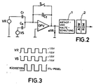
- the capacitive element C s in the preferred embodiment is a capacitive MOS element whose metal layer consists of palladium, which is also referred to as a MOS palladium gate sensor.
- the capacitive element C s is supplied by a first voltage source VS with a square wave voltage, the amplitude of which corresponds to +/- 1.5 V at a duty cycle of 50% in a preferred embodiment.
- the capacitive element C s is connected to the inverting input of an operational amplifier OPV.
- a second voltage source VR generates a second square-wave signal which corresponds to the first square-wave signal but is inverted with respect to this.
- This second square-wave voltage signal is applied to a reference capacitor C r , the output of which is also connected to the inverting input of the operational amplifier OPV.
- the capacitance of the reference capacitor C r is selected such that an offset voltage appearing at the output of the operational amplifier is compensated for with the capacitance-voltage characteristic of the capacitive element C s unaffected by the variable to be measured.
- the operational amplifier OPV In the feedback branch of the operational amplifier OPV, ie between its output and its inverting input, there is an integration capacitor C f , to which an electronic switch S is connected in parallel.
- the electronic switch S is operated in a specific, fixed phase dependence on the phase of the first square-wave signal by means of a reset signal (see FIG. 3), as a result of which the integration is ended and a voltage value at the output ⁇ VA is reset.
- the output value of the operational amplifier OPV ⁇ VA before the reset is taken over in a sample and hold circuit 1.
- the influencing variable can be derived from this initial value, which is the H2 concentration in the example.
- the assignment of the H2 concentration to the output voltage ⁇ VA is expediently carried out via a table which is generated by a D / A converter a ROM 2 can be implemented in which the dependency of the quantities mentioned, which is shown in FIG.
- the curve shown in FIG. 4 is the result of a measurement with a palladium sensor, the catalytic metal layer of which is a 21.1 nm thick palladium layer which is arranged on a 34 nm thick silicon dioxide layer.
- a capacitive MOS structure with a 104.5 nm thick gold gate on a 34 nm thick silicon dioxide insulator layer was chosen as the reference capacitor.
- the capacitance of the integration capacitor C f is 1 nF.
- the capacitance value C f must be selected so that the operational amplifier OPV is not overdriven when the measured variable is at its maximum.
- the method according to the invention for measuring the variable influencing the capacitance-voltage characteristic enables compensation of disturbance variables which affect both the actual sensor element or capacitive element C s and the reference capacitor C r influence in the same way in their capacity-voltage characteristics.
- the capacitive (sensor) element C s has both a dependence of the capacitance-voltage characteristic on a variable A and on a disturbance variable B
- this undesirable sensitivity to the disturbance variable B can be compensated for by the fact that a reference capacitor capacitive MOS element is used, which is only sensitive to the disturbance variable B.
- a complete compensation against the disturbance variable B is possible.
- a large number of reference elements can be used to compensate for a corresponding number of undesirable cross-sensitivities.
- the frequency of the square-wave signals is preferably in the kHz range.
- the period of the square wave signals is longer than the minority carrier response time, so that the minority carrier accumulation is in an equilibrium state, while the period of the rectangular voltage signals is shorter than the minority generation recombination time, so that the MOS structure is not in equilibrium -Inversion area device. This leads to an amplification of the signal, since the voltage-dependent capacitance curve runs down into the area of deep charge carrier depletion.
- T 2 ⁇ N B / n i , where ⁇ denotes the minority carrier lifetime, N B the doping and n i the intrinsic concentration for the relevant MOS capacitor.
- a capacitive MOS structure with a palladium gate is used as the moisture sensor.
- the method according to the invention can also be used for gas sensors with a MOS structure for evaluating the gas concentration as well as for measuring other variables influencing the capacitance-voltage characteristic of a capacitive element.
Landscapes
- Chemical & Material Sciences (AREA)
- Physics & Mathematics (AREA)
- General Physics & Mathematics (AREA)
- Analytical Chemistry (AREA)
- Electrochemistry (AREA)
- Chemical Kinetics & Catalysis (AREA)
- Health & Medical Sciences (AREA)
- Life Sciences & Earth Sciences (AREA)
- Engineering & Computer Science (AREA)
- Biochemistry (AREA)
- General Health & Medical Sciences (AREA)
- Power Engineering (AREA)
- Immunology (AREA)
- Pathology (AREA)
- Investigating Or Analyzing Materials By The Use Of Electric Means (AREA)
- Measurement Of Resistance Or Impedance (AREA)
Applications Claiming Priority (2)
| Application Number | Priority Date | Filing Date | Title |
|---|---|---|---|
| DE3915563 | 1989-05-12 | ||
| DE3915563A DE3915563C1 (enExample) | 1989-05-12 | 1989-05-12 |
Publications (2)
| Publication Number | Publication Date |
|---|---|
| EP0471684A1 EP0471684A1 (de) | 1992-02-26 |
| EP0471684B1 true EP0471684B1 (de) | 1993-12-15 |
Family
ID=6380539
Family Applications (1)
| Application Number | Title | Priority Date | Filing Date |
|---|---|---|---|
| EP90906167A Expired - Lifetime EP0471684B1 (de) | 1989-05-12 | 1990-04-17 | Schaltung und verfahren zum messen einer die kapazitäts-spannungs-charakteristik eines kapazitiven elementes beeinflussenden grösse |
Country Status (6)
| Country | Link |
|---|---|
| US (1) | US5235267A (enExample) |
| EP (1) | EP0471684B1 (enExample) |
| JP (1) | JPH0740057B2 (enExample) |
| KR (1) | KR930011421B1 (enExample) |
| DE (2) | DE3915563C1 (enExample) |
| WO (1) | WO1990013793A1 (enExample) |
Families Citing this family (19)
| Publication number | Priority date | Publication date | Assignee | Title |
|---|---|---|---|---|
| DE4211907A1 (de) * | 1991-04-19 | 1992-11-05 | Rene Baltus | Vorrichtung zum messen oder sammeln der menge eines in einer fluessigkeit enthaltenen gasanteils oder feststoffes |
| DK167823B1 (da) * | 1991-06-18 | 1993-12-20 | Asger Gramkow | Apparat til registrering af et koelemiddels fugtigheds- og syreindhold |
| US5514337A (en) * | 1994-01-11 | 1996-05-07 | American Research Corporation Of Virginia | Chemical sensor using eddy current or resonant electromagnetic circuit detection |
| JP2561040B2 (ja) * | 1994-11-28 | 1996-12-04 | 日本電気株式会社 | 容量型センサの容量変化検出回路およびその検出方法 |
| US5792938A (en) * | 1996-12-13 | 1998-08-11 | Panametrics, Inc. | Humidity sensor with differential thermal detection and method of sensing |
| DE10134680A1 (de) * | 2001-07-20 | 2003-02-06 | Endress & Hauser Gmbh & Co Kg | Schaltungsanrdnung für einen kapazitiven Sensor |
| DE10330742A1 (de) * | 2003-07-07 | 2005-01-27 | Daimlerchrysler Ag | Abgassensor zur Detektion einer Gaskomponente im Abgas einer Brennkraftmaschine und Verfahren zum Betreiben eines Abgassensors |
| US7901553B2 (en) * | 2004-01-27 | 2011-03-08 | H2Scan Corporation | Method and system for sensing gas incorporating an integrated reference element |
| WO2006002301A1 (en) * | 2004-06-21 | 2006-01-05 | Kele, Inc. | Measuring the capacitance of a capacitive sensor with a microprocessor |
| JP4770530B2 (ja) * | 2006-03-13 | 2011-09-14 | 株式会社デンソー | 容量式湿度センサ |
| CN101738422B (zh) * | 2009-12-23 | 2012-09-05 | 北京宝力马传感技术有限公司 | 一种湿度测量装置及方法 |
| US9678055B2 (en) | 2010-02-08 | 2017-06-13 | Genia Technologies, Inc. | Methods for forming a nanopore in a lipid bilayer |
| US9605307B2 (en) | 2010-02-08 | 2017-03-28 | Genia Technologies, Inc. | Systems and methods for forming a nanopore in a lipid bilayer |
| US8962242B2 (en) | 2011-01-24 | 2015-02-24 | Genia Technologies, Inc. | System for detecting electrical properties of a molecular complex |
| US8986629B2 (en) | 2012-02-27 | 2015-03-24 | Genia Technologies, Inc. | Sensor circuit for controlling, detecting, and measuring a molecular complex |
| US9759711B2 (en) | 2013-02-05 | 2017-09-12 | Genia Technologies, Inc. | Nanopore arrays |
| US9551697B2 (en) | 2013-10-17 | 2017-01-24 | Genia Technologies, Inc. | Non-faradaic, capacitively coupled measurement in a nanopore cell array |
| KR102237710B1 (ko) * | 2014-06-18 | 2021-04-09 | 주식회사 해치텍 | 커패시터형 습도센서 |
| US9465001B2 (en) | 2014-09-15 | 2016-10-11 | Bourns, Inc. | Conductive liquid property measurement using variable phase mixing |
Family Cites Families (10)
| Publication number | Priority date | Publication date | Assignee | Title |
|---|---|---|---|---|
| US4112356A (en) * | 1976-12-20 | 1978-09-05 | Toy Stephen M | Semiconductor gas detector circuit |
| US4149231A (en) * | 1977-05-04 | 1979-04-10 | Bunker Ramo Corporation | Capacitance-to-voltage transformation circuit |
| US4166974A (en) * | 1978-01-23 | 1979-09-04 | The United States Of America As Represented By The Secretary Of The Navy | Apparatus and method for measuring capacitive energy |
| FR2485224A1 (fr) * | 1980-06-19 | 1981-12-24 | Cii Honeywell Bull | Capteur de position de bande et dispositif de mesure de position incluant ce capteur |
| JPS60128345A (ja) * | 1983-12-15 | 1985-07-09 | Olympus Optical Co Ltd | イオン濃度測定装置 |
| US4636714A (en) * | 1984-01-18 | 1987-01-13 | Wystron, Inc. | Capacitive transducer and method |
| DE3413849C2 (de) * | 1984-02-21 | 1986-07-10 | Dietrich 8891 Obergriesbach Lüderitz | Kapazitäts-Meßgerät |
| JPS60242354A (ja) * | 1984-05-16 | 1985-12-02 | Sharp Corp | Fet型センサ |
| US4831325A (en) * | 1987-04-01 | 1989-05-16 | General Signal Corporation | Capacitance measuring circuit |
| US5103183A (en) * | 1990-01-26 | 1992-04-07 | Rockwell International Corporation | Method of profiling compensator concentration in semiconductors |
-
1989
- 1989-05-12 DE DE3915563A patent/DE3915563C1/de not_active Expired - Lifetime
-
1990
- 1990-04-17 KR KR1019900702097A patent/KR930011421B1/ko not_active Expired - Fee Related
- 1990-04-17 JP JP2505963A patent/JPH0740057B2/ja not_active Expired - Lifetime
- 1990-04-17 DE DE90906167T patent/DE59003905D1/de not_active Expired - Fee Related
- 1990-04-17 US US07/768,440 patent/US5235267A/en not_active Expired - Fee Related
- 1990-04-17 EP EP90906167A patent/EP0471684B1/de not_active Expired - Lifetime
- 1990-04-17 WO PCT/EP1990/000612 patent/WO1990013793A1/de not_active Ceased
Non-Patent Citations (2)
| Title |
|---|
| NTIS Tech. Notes, August 1987, Springfield, VA, US, pages 729-730, B.D. Bryner et al: "Sliding capacitve displacement transducer" * |
| Transactions of the Institute of Electronics, Information & Communication Engineers, vol. E70, no. 11, November 1987, Tokyo, JP, pages 1049-1050; T. Nagasawa et al: "An interface circuit for capacitive sensors" * |
Also Published As
| Publication number | Publication date |
|---|---|
| DE59003905D1 (de) | 1994-01-27 |
| EP0471684A1 (de) | 1992-02-26 |
| KR930011421B1 (ko) | 1993-12-06 |
| JPH04503112A (ja) | 1992-06-04 |
| US5235267A (en) | 1993-08-10 |
| KR920700405A (ko) | 1992-02-19 |
| DE3915563C1 (enExample) | 1990-10-25 |
| JPH0740057B2 (ja) | 1995-05-01 |
| WO1990013793A1 (de) | 1990-11-15 |
Similar Documents
| Publication | Publication Date | Title |
|---|---|---|
| EP0471684B1 (de) | Schaltung und verfahren zum messen einer die kapazitäts-spannungs-charakteristik eines kapazitiven elementes beeinflussenden grösse | |
| EP0365622B1 (de) | Verfahren zum zerstörungsfreien messen magnetischer eigenschaften eines prüfkörpers sowie vorrichtung zum zerstörungsfreien messen magnetischer eigenschaften eines prüfkörpers | |
| DE2711767A1 (de) | Vorrichtung fuer die temperaturmessung | |
| DE2615757A1 (de) | Verfahren und anwendung zum messen der oberflaechenzustaende in metall-isolator- halbleiterstrukturen | |
| EP1616174A1 (de) | Vorrichtung zum betreiben eines gassensors | |
| EP1222454B1 (de) | Verfahren und einrichtung zur bestimmung der gaskonzentrationen in einem gasgemisch | |
| DE19639627A1 (de) | Kompensation für räumliche und zeitliche Temperaturschwankungen in einem Wärmeleitfähigkeitsdetektor | |
| EP0048862A1 (de) | Verfahren zur Messung von Widerständen und Kapazitäten von elektronischen Bauelementen | |
| WO2023078623A1 (de) | Verfahren und einrichtung zum ermitteln dynamischer parameter einer mems-vorrichtung, und mems-vorrichtung | |
| DE3438546A1 (de) | Verfahren zum nachweis eines stoffes oder zum nachweis zumindest einer komponente eines stoffgemisches sowie schwingkondensator zur durchfuehrung des verfahrens | |
| DE10029795C2 (de) | Vorrichtung zum Messen des Innenwiderstandes einer linearen Lambdasonde | |
| EP1037022A1 (de) | Verfahren zur Bestimmung der Strömungsgeschwindigkeit oder der Molmasse von Flüssigkeiten | |
| DE19755417C2 (de) | Auswerteschaltung zur Ermittlung komplexer Impedanzen, Vorrichtung zur Messung komplexer Impedanzen und Verwendung der Vorrichtung | |
| DE69722926T2 (de) | Vorrichtung und verfahren zur feststellung eines fluids | |
| DE4229558C2 (de) | Beschleunigungsaufnehmer | |
| DE2208778C3 (de) | Selbsttätige Isolationsprüfeinrichtung | |
| DE4014395A1 (de) | Schaltung und verfahren zum messen einer die kapazitaets-spannungs-charakteristik eines kapazitiven elementes beeinflussenden groesse | |
| DE4401570A1 (de) | Einrichtung für die Messung von Zustandsgrößen in Gasen mit zumindest einem Halbleiter-Gassensor | |
| DE19811069C2 (de) | Meßschaltung zur Ermittlung der Konzentration eines oder mehrerer Gase in einem Gasgemisch | |
| DE68923699T2 (de) | Dünnfilmfeuchtigkeitprüfelemente und verfahren zur herstellung. | |
| DE19851409C2 (de) | Verfahren zur Bestimmung des Nullpunktfehlers eines Akzelerometers | |
| DE2705624A1 (de) | Messgeraet | |
| DE102018124090A1 (de) | Elektronische Schaltung für einen elektrochemischen Sensor und Verfahren zur Messung einer Impedanz von mindestens einem Messkanal des elektrochemischen Sensors | |
| DE2021811C3 (de) | Einrichtung zur Messung der Dielektrizitätskonstanten von Stoffen | |
| DE4210164A1 (de) | Verfahren und Schaltungsanordnung zum Fernmessen von Zuständen |
Legal Events
| Date | Code | Title | Description |
|---|---|---|---|
| PUAI | Public reference made under article 153(3) epc to a published international application that has entered the european phase |
Free format text: ORIGINAL CODE: 0009012 |
|
| 17P | Request for examination filed |
Effective date: 19910424 |
|
| AK | Designated contracting states |
Kind code of ref document: A1 Designated state(s): CH DE FR GB LI NL |
|
| 17Q | First examination report despatched |
Effective date: 19930524 |
|
| GRAA | (expected) grant |
Free format text: ORIGINAL CODE: 0009210 |
|
| AK | Designated contracting states |
Kind code of ref document: B1 Designated state(s): CH DE FR GB LI NL |
|
| GBT | Gb: translation of ep patent filed (gb section 77(6)(a)/1977) |
Effective date: 19931215 |
|
| REF | Corresponds to: |
Ref document number: 59003905 Country of ref document: DE Date of ref document: 19940127 |
|
| ET | Fr: translation filed | ||
| PLBE | No opposition filed within time limit |
Free format text: ORIGINAL CODE: 0009261 |
|
| STAA | Information on the status of an ep patent application or granted ep patent |
Free format text: STATUS: NO OPPOSITION FILED WITHIN TIME LIMIT |
|
| 26N | No opposition filed | ||
| PGFP | Annual fee paid to national office [announced via postgrant information from national office to epo] |
Ref country code: DE Payment date: 19980523 Year of fee payment: 9 |
|
| PGFP | Annual fee paid to national office [announced via postgrant information from national office to epo] |
Ref country code: FR Payment date: 19980527 Year of fee payment: 9 |
|
| PGFP | Annual fee paid to national office [announced via postgrant information from national office to epo] |
Ref country code: CH Payment date: 19980529 Year of fee payment: 9 |
|
| PGFP | Annual fee paid to national office [announced via postgrant information from national office to epo] |
Ref country code: NL Payment date: 19980531 Year of fee payment: 9 |
|
| PGFP | Annual fee paid to national office [announced via postgrant information from national office to epo] |
Ref country code: GB Payment date: 19980612 Year of fee payment: 9 |
|
| PG25 | Lapsed in a contracting state [announced via postgrant information from national office to epo] |
Ref country code: GB Free format text: LAPSE BECAUSE OF NON-PAYMENT OF DUE FEES Effective date: 19990417 |
|
| PG25 | Lapsed in a contracting state [announced via postgrant information from national office to epo] |
Ref country code: LI Free format text: LAPSE BECAUSE OF NON-PAYMENT OF DUE FEES Effective date: 19990430 Ref country code: CH Free format text: LAPSE BECAUSE OF NON-PAYMENT OF DUE FEES Effective date: 19990430 |
|
| PG25 | Lapsed in a contracting state [announced via postgrant information from national office to epo] |
Ref country code: NL Free format text: LAPSE BECAUSE OF NON-PAYMENT OF DUE FEES Effective date: 19991101 |
|
| GBPC | Gb: european patent ceased through non-payment of renewal fee |
Effective date: 19990417 |
|
| REG | Reference to a national code |
Ref country code: CH Ref legal event code: PL |
|
| PG25 | Lapsed in a contracting state [announced via postgrant information from national office to epo] |
Ref country code: FR Free format text: LAPSE BECAUSE OF NON-PAYMENT OF DUE FEES Effective date: 19991231 |
|
| NLV4 | Nl: lapsed or anulled due to non-payment of the annual fee |
Effective date: 19991101 |
|
| REG | Reference to a national code |
Ref country code: FR Ref legal event code: ST |
|
| PG25 | Lapsed in a contracting state [announced via postgrant information from national office to epo] |
Ref country code: DE Free format text: LAPSE BECAUSE OF NON-PAYMENT OF DUE FEES Effective date: 20000201 |